MACOM CDMA900 Datasheet

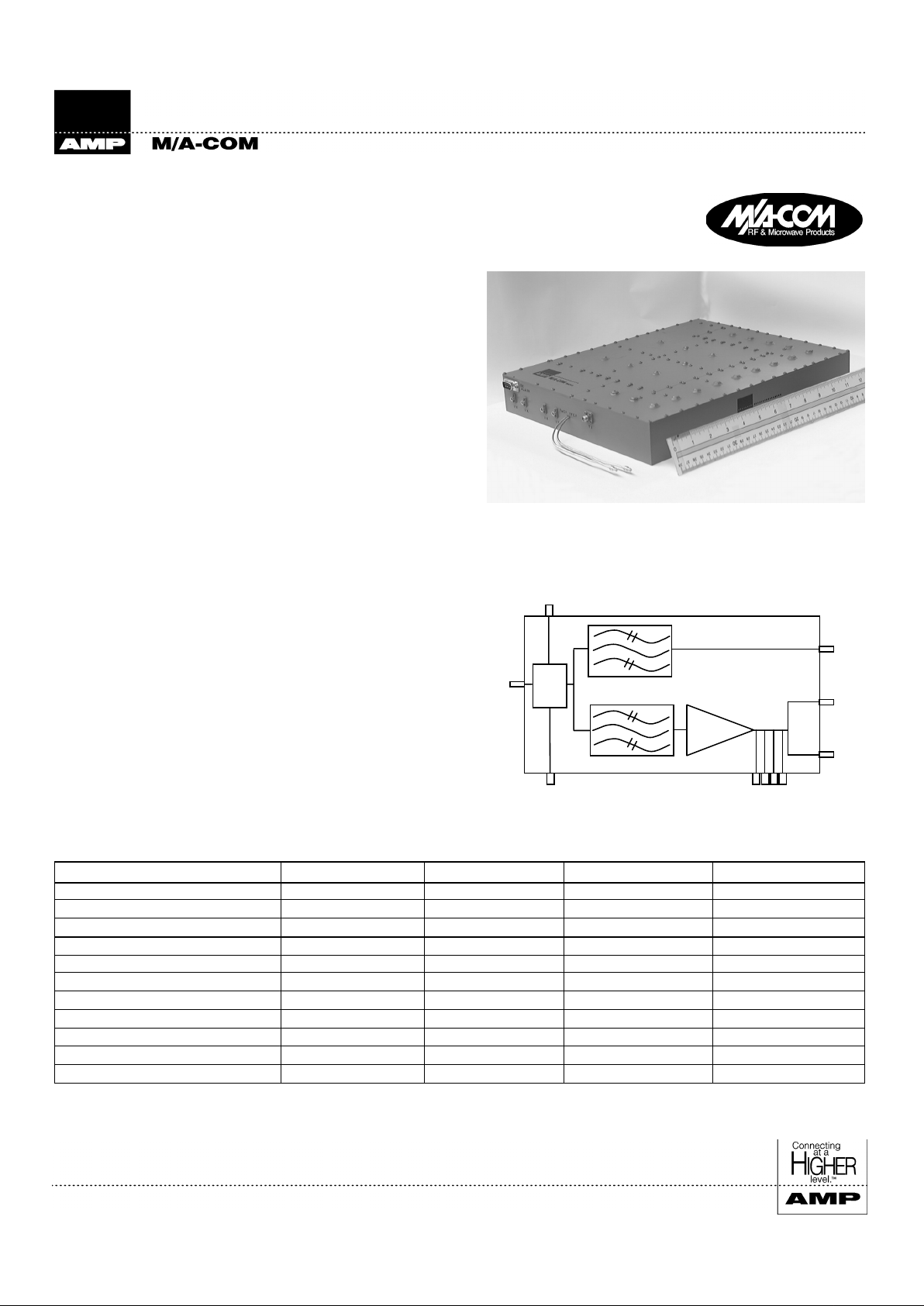
CDMA 900 MHz Diplexer/LNA
M/A-COM Division of AMP Incorporated ■ North America: Tel. (800) 366-2266, Fax (800) 618-8883 ■ Asia/Pacific: Tel.+85 2 2111 8088, Fax +85 2 2111 8087
■
Europe: Tel. +44 (1344) 869 595, Fax+44 (1344) 300 020
www.macom.com
AMP and Connecting at a Higher Level are trademark s.
The preliminary spec ifications data sheet c ontains typical electrical specifications which may change prior to final introduction.
V1.00
Features
• TX Passband 843 - 870 MHz
• RX Passband 915.325-924.675 MHz
• Low Transmit Insertion Loss < 0.6 dB
• Low Receive Noise Figure < 3.0 dB
• Typical Receive Path Gain 13 dB
• Typical Return Loss 18 dB
• RX to TX Rejections 85 dB
• TX to RX Rejections 97 dB to 3.0 GHz
• 1dB Compression Point +3.5dBm, typical
• Input Intercept Point +13dBm (Pin = -2 dBm)
• LNA Alarm Circuit
• Compact Size 13.39 x 10.63 x 2.05 inch
Description
M/A-COM’s CDMA 900 Filter/LNA is ideally suited for all
Basestation applications. The filter performance allows for 97dB
rejection at 898 MHz, while the balanced LNA possesses
excellent intermodulation performance, low noise figure and
controllable gain.
Custom models can be designed to fit other electrical and
mechanical requirements.
Typical Electrical Specifications1, TA= +25ºC
Parameters Units Min. Typ. Max.
TX Path
Insertion Loss
dB 0.5 0.55 0.6
Return Loss
dB 15 18 22
Rejection at RX Band
dB 95 97 105
RX PATH
Gain dB 12 13.5 15
Return Loss dB 15 18 20
Noise Fi
g
ure dB 2.2 2.4 3.0
Input Third Order Intercept dBm +12 +13 +15
1dB Compression Point dBm +3.0 +3.5 +4
Power and Current V, mA 5, 170 5, 180 5, 190
CDMA 900 MHz Diplexer/LNA
Preliminary Specifications
Functional Diagram
TX
Ant
RX
RX
LNA
FWD
FWD
DC & Alarm
D.C.

CDMA 900 MHz Diplexer/LNA
M/A-COM Division of AMP Incorporated ■ North America: Tel. (800) 366-2266, Fax (800) 618-8883 ■ Asia/Pacific: Tel.+85 2 2111 8088, Fax +85 2 2111 8087
■
Europe: Tel. +44 (1344) 869 595, Fax+44 (1344) 300 020
www.macom.com
AMP and Connecting at a Higher Level are trademark s.
The preliminary spec ifications data sheet c ontains typical electrical specifications which may change prior to final introduction.
V1.00
Absolute Maximum Ratings
1
Parameter Absolute Maximum
Input Power
1
Operating Temperature
Stora
g
e Temperature
5 W CW
-25°C to +65°C
-65°C to 150°C
1. Exceeding these limits may cause permanent damage.
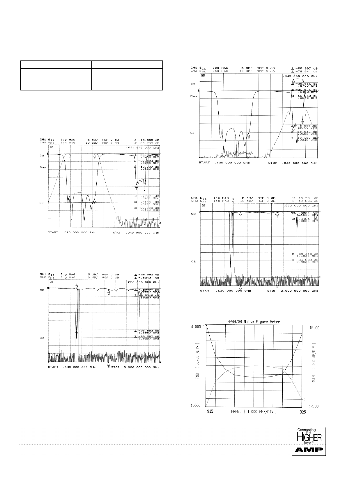
Typical Performance @ +25°C
TX Path
S11 & S21 vs. Frequency
RX Path
S11 & S21 vs. Frequency
RX Path
Rejections to 3 GHz
RX Path
Noise Figure & Gain
TX Path
Rejections to 3 GHz
 Loading...