MACOM AT-108TR, AT-108RTR, AT-108 Datasheet

Voltage Variable Absorptive Attenuator
Voltage Variable Absorptive Attenuator
Voltage Variable Absorptive AttenuatorVoltage Variable Absorptive Attenuator
40 dB, 0.5
40 dB, 0.5————3.0 GHz
40 dB, 0.540 dB, 0.5
3.0 GHz
3.0 GHz3.0 GHz
Features
• Single Positive Voltage Control 0 to +5 Volts
• 40 dB Attenuation Range at 900 MHZ GHz
• ± 2 dB Linearity from BSL
• Low DC Power Consumption
• Low-Cost SOIC-8 Plastic Package
• Tape and Reel Packaging Available
Description
M/A-COM’s AT-108 is a GaAs, MESFET MMIC voltage
variable absorptive attenuator in a low cost SOIC-8 lead surface
mount plastic package. The AT-108 is ideally suited for use
where linear attenuation fine tuning and very low power
consumption are required. Typical applications include radio,
cellular, GPS equipment and automatic gain/level control
circuits.
The AT-108 is fabricated with a monolithic GaAs MMIC using
a mature 1-micron process. The process features full chip
passivation for increased performance and reliability.
AT-108
1
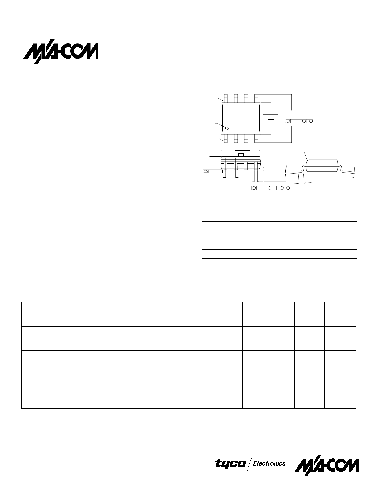
SOIC-8
PIN 8
Oreintation
Mark
.0532/.0688
(1.35/1.75)
.004
1. Dimensions are in inches/mm.
Ordering Information
AT-108 SOIC-8 Lead Plastic Package
AT-108TR Forward Tape and Reel
AT-108RTR Reverse Tape and Reel
1. If specific reel size is required, consult factory for part number
assignment.
PIN 1
(0.10)
.050 (1.27)
.1890/.1968
(4.80/5.00)
-A-
BSC.
.1497/.1574
(3.80/4.00)
.0040/.0098
.010(.25)
-C-
.013/. 02 0 (8
-B-
(.10/.25)
(.33/.51)
PL)
C A B
M M S
.2284/.2440
(5.80/6.20)
.010(.25)
CHAMFER
(OPTIONAL
)
0°/80°
Part Number Package
M M B
.016/.050
(0.40/1.27)
.0075/.0098
1
1
(.19/.25)
Electrical Specifications: TA = 25°C
Parameter Test Conditions
1
====
1
Units Min. Typ. Max.
Insertion Loss 0.5 - 1.0 GHz dB 2.5 2.7
1.0 - 3.0 GHz dB 3.2 3.5
Attenuation 0.5 - 1.0 GHz dB 40
1.0 - 2.0 GHz dB 35
2.0 - 3.0 GHz dB 28
Flatness 0.5 - 1.0 GHz dB ±0.5 ±0.8
(Peak-to-Peak) 1.0 - 2.0 GHz dB ±1.2 ±1.5
2.0 - 3.0 GHz dB ±1.5 ±1.8
VSWR 0.5 - 3.0 GHz 2:1
T
, T
rise
fall
Ton, T
off
Transients
1. All measurements in a 50Ω system.
Specifications subject to change without notice.
North America: Tel. (800) 366-2266, Fax (800) 618-8883
Asia/Pacif ic: Tel.+81-44-844-8296, Fax +81-44-844-8298
Europe: Tel. +44 (1344) 869 595, Fax+44 (1344) 300 020
Visit www.macom.com for additional data sheets and product information.
10% to 90% RF, 90% to 10% RF µs 15
50% Control to 90% RF, Control to 10% RF µs 25
In-band mV 12
V 4.0

Voltage Variable Absorp tive Attenu ator, 40 dB, 0.5-3.0 GHz
AT-108
Absolute Maximum Ratings
1
Parameter Absolute Maximum
Maximum Input Power +21 dBm
Supply Voltage V
Control Voltage V
CC
C
-1V, +8V
-1V, VCC + 0.5V
Operating Temperature -40°C to +85°C
Storage Temperature -65°C to +150°C
1. Operation of this device above any one of these parameters
may cause permanent damage.
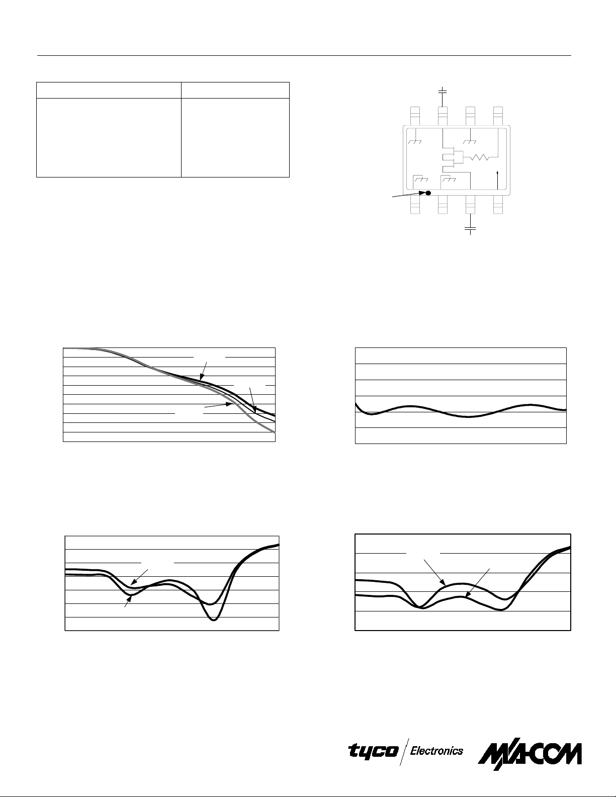
Typical Performance Curves
Attenuation vs. Control Voltage @ +25°C
0
-5
-10
-15
-20
-25
-30
-35
Attenuation (dB)
-40
-45
-50
5 4.5 4 3.5 3 2.5 2 1.5 1 0.5 0
Control Voltage (Volts)
2200MHz
1800MHz
900MHz
Functional Schematic
GND RF GND Vc
8
PIN
Orientation Mark
1
GND
76
GND
RF
5
32
4
Vcc
1. VCC = +5 VDC @ 50 µA max.
= 0 VDC to +5 VDC @ 50 µA max.
2. V
C
3. External DC blocking capacitors are required on all RF ports.
4. 39pF used for data measurements.
Insertion Loss vs. Frequency
-1.6
-1.8
-2
-2.2
-2.4
-2.6
Insertion Loss (dB)
-2.8
0
0.5
0.66
0.82
0.97
1.13
1.6
1.28
1.44
Frequency (GHz)
1.75
1.91
2.06
2.22
2.38
2.53
2.69
2.84
Return Loss vs. Control Voltage @ +25°C
F = 900 MHz
0
-5
-10
-15
-20
-25
Return Loss (dB)
-30
-35
54.543.532.521.510.50
Specifications subject to change without notice.
Input RL
North America: Tel. (800) 366-2266, Fax (800) 618-8883
Asia/Pacif ic: Tel.+81-44-844-8296, Fax +81-44-844-8298
Europe: Tel. +44 (1344) 869 595, Fax+44 (1344) 300 020
Visit www.macom.com for additional data sheets and product information.
Output RL
Control Voltage (Volts)
Return Loss vs. Control Voltage @ +25°C
F = 1800 MHz
0
-5
-10
-15
Return Loss (dB)
-20
-25
5 4.5 4 3.5 3 2.5 2 1.5 1 0.5 0
Input RL
Output RL
Control Voltage (Volts)
V 4.0
 Loading...