MACOM AT10-0019TR, AT10-0019-TB, AT10-0019 Datasheet

PIN Diode Based Variable
Attenuator, 50 - 1000 MHz
V 5.00
AT10-0019
Features
n High Dynamic Range: 42dB Typical
n Flat Attenuation vs. Frequency
n High P1dB Compression
n Operates on a Single +5V Supply:
n SOW-16, Wide Body Package
n 50 Ohm Nominal Impedance
Description
M/A-COM's AT10-0019 is a Voltage Controlled PIN diode
based π attenuator packaged in a low cost, 16 lead wide
body plastic SMT package. The PIN diode design makes
this part well suited for applications where low distortion or
high linear operating power levels are required. These
attenuators are ideal for gain control in multi-channel
digital communications systems.
Absolute Maximum Ratings 1
Parameter Absolute Maximum
Max. Input Power
50 - 500 MHz
500 - 1000 MHz
Voltages
V
CC
Control Voltage
Operating Temperature -40°C to +85°C
Storage Temperature -65°C to +125°C
+24 dBm
+30 dBm
-1 V to +7.0 V
-1 V to +15 V
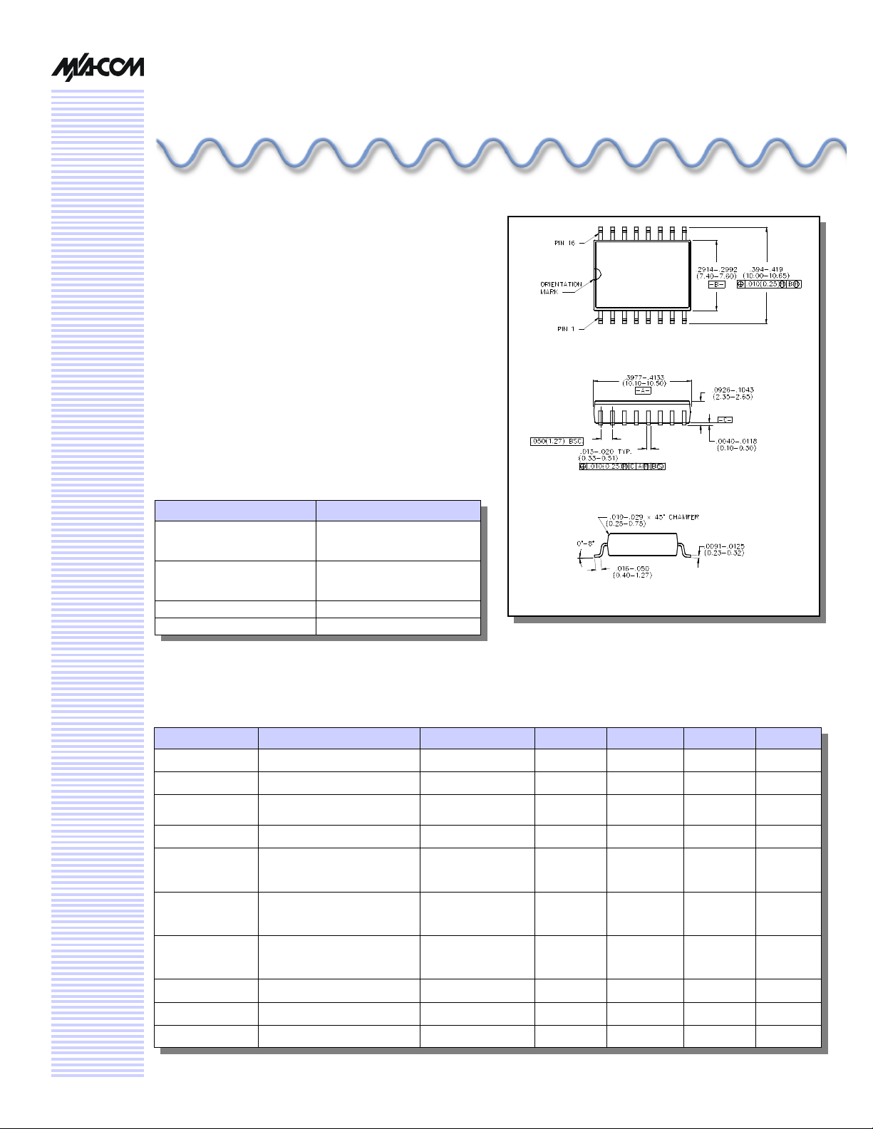
SOW-16
Package outline conforms to JEDEC standard MS-013AA.
1. Operation of this device above any one of these parameters
may cause permanent damage.
Electrical Specifications2: TA = 25°C
Parameter Test Conditions Frequency Units Min Typical Max
Insertion Loss Vcont.: +10 V 50 - 1000 MHz dB — 2.4 2.8
Dynamic Range Vcont.: 0 V 50 - 1000 MHz dB 33 42 —
Attenuation
Flatness
VSWR Vcont.: 0 - 10V 50 - 1000 MHz Ratio — 1.7:1 2.1:1
Trise, Tfall
Ton, Toff
Transients
1 dB
Compression
Input IP3 Vcont.: 0 - 10V
VCC — — V +4.75 +5.0 +5.25
I CC VCC = 5.25 V DC mA — 2 2.5
Control Current — DC mA — 2.7 3.5
Attenuation: 0 to 20 dB
Attenuation: 20 to 30 dB
10%/90%, 90%/10%
50% Cntl to 90%/10% RF
In-band
Vcont.: 0 - 10V 100 MHz
Two-tone inputs up to +10
dBm
50 - 1000 MHz
50 - 1000 MHz
— µS
500 MHz
1000 MHz
100 MHz
1000 MHz
dB
dB
µS
mV
dBm
dBm
dBm
dBm
dBm
—
—
—
—
—
10
17
21
24
34
1.0
1.5
10
15
150
13
20
24
27
37
1.5
2.0
20
25
250
—
—
—
—
—
2. Unit requires external .01 µF DC Blocks on RF lines.

PIN Diode Based Variable Attenuator, 50 - 1000 MHz
Attenuation (dB)
AT10-0019
V 5.00
Pin Configuration
Pin # Function Pin # Function
1 GND 9 GND
2 RF in 10 V control
3 GND 11 GND
4 GND 12 GND
5 GND 13 GND
6 GND 14 GND
7 V Supply 15 RF out
8 GND 16 GND
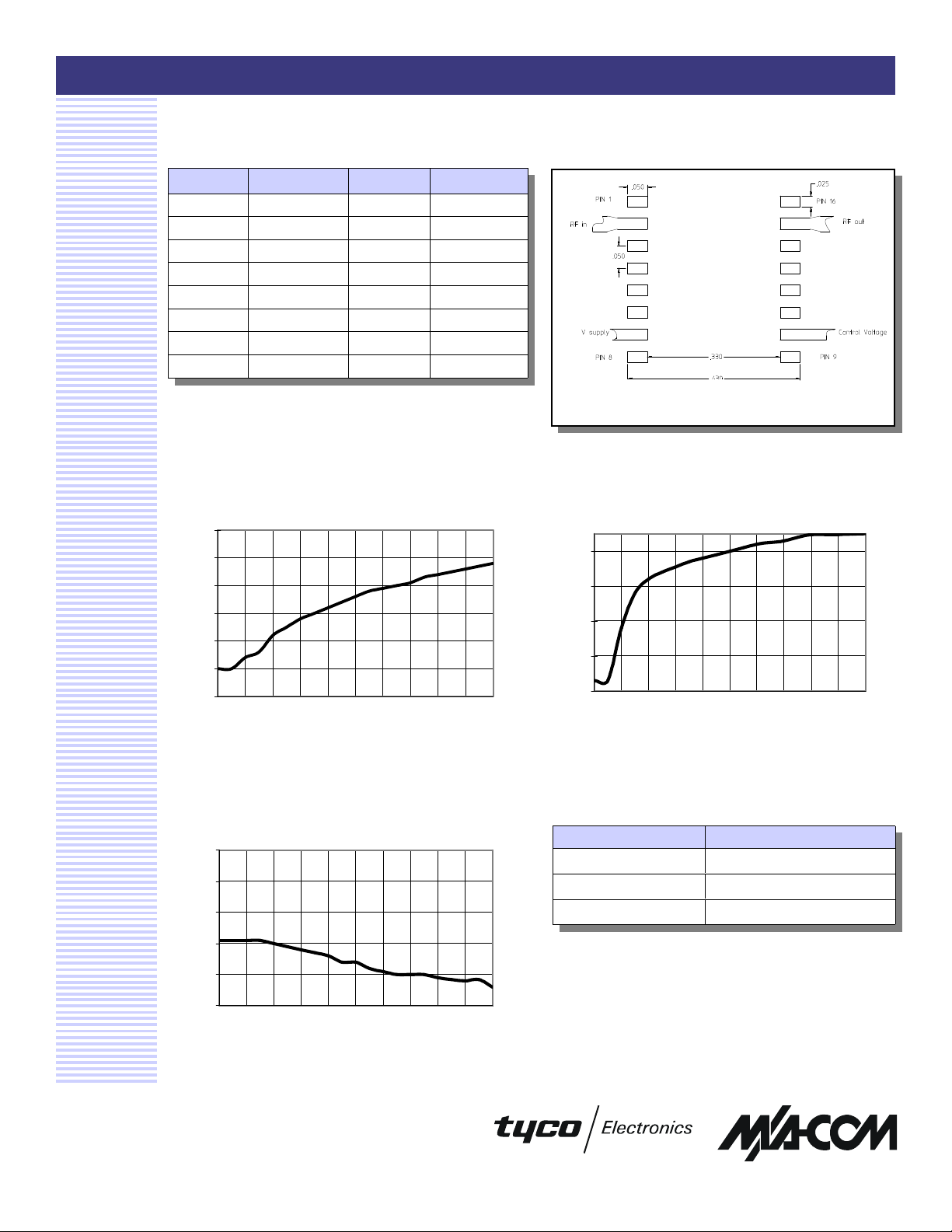
Typical Performance Curves
Attenuation vs. Frequency
@ Control Voltage = 0V
-30
-35
-40
Pad Layout
AT10-0019
PAD LAYOUT
Dimensions are in inches
All undefined pins are connected to ground
Attenuation vs. Control Voltage
@ 500 MHz
-5
-15
-45
-50
Attenuation (dB)
-55
-60
50 145 240 335 430 525 620 715 810 905 1000
Frequency (MHz)
Insertion Loss vs. Frequency
@ Control Voltage = 10V
0.0
-0.5
-1.0
-1.5
IL (dB)
-2.0
-2.5
50 145 240 335 430 525 620 715 810 905 1000
Frequency (MHz)
-25
-35
-45
0 1 2 3 4 5 6 7 8 9 10
Control Voltage (V)
Ordering Information
Part Number Package
AT10-0019 Bulk Packaging
AT10-0019TR Tape and Reel (1K Reel)
AT10-0019-TB Unit Mounted on Test Board
Specifications subject to change without notice.
n North America: Tel. (800) 366-2266
n Asia/Pacific: Tel.+81-44-844-8296, Fax +81-44-844-8298
n Europe: Tel. +44 (1344) 869 595, Fax+44 (1344) 300 020
Visit www.macom.com for additional data sheets and product information.
2
 Loading...