0.5 W, 2.4 GHz Power Amplifier
V 1.4
AM52-0024
Features
• Ideal for 802.11b ISM Applications
• Single Positive Supply
• Output Power 27.5 dBm
• 57% Typical Power Added Efficiency
• Downset MSOP-8 Package
Description
M/A-COM’s AM52-0024 is a 0.5 W, 2.4 GHz GaAs
MMIC, power amplifier in a low-cost MSOP-8 package. It
employs some external matching to obtain optimum input
return loss and output power performance. The AM520024 may be operated with supply voltages of +3.3 V to
+5.5 V.
The AM52-0024 may be used in a wide variety of applic ations including WLAN, WDECT, and Bluetooth.
The AM52-0024 is fabricated using M/A-COM’s SelfAligned MSAG MESFET process to realize high power
efficiency, single supply voltage, and small size. The process features full passivation for increased performance and
reliability.
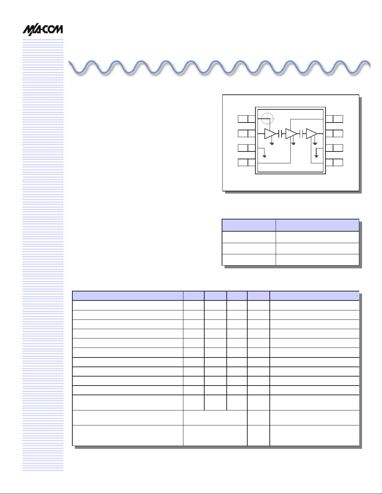
Functional Schematic
PIN 1
PIN 8
Ordering Information
Part Number Package
AM52-0024TR 7 inch, 1000 Piece Reel
AM52-0024TR-3000 13 inch, 3000 Piece Reel
AM52-0024SMB Sample Test Board
Electrical Specifications
Characteristic Min Typ Max Unit Test Conditions
Frequency 2.4 2.5 GHz
Output Power 25.5 27.5 dBm F = 2450 MHz, PIN = -2 dBm
Power Added Efficiency 57 % F = 2450 MHz, PIN = -2 dBm
Current Under Drive 300 mA F = 2450 MHz, PIN = -2 dBm
Current Under Linear Operation 130 230 300 mA F = 2450 MHz, P
Small Signal Gain 29.0 dB F = 2450 MHz, P
Harmonics -40 dBc F = 2450 MHz, PIN = -2 dBm
Input VSWR 1.4:1 2.0:1 - F = 2450 MHz, PIN = -2 dBm
Off Isolation 40 dB F = 2450 MHz, VDD = 0 V
Thermal Resistance, junction to package bottom 25 °C/W F = 2450 MHz, PIN = -2 dBm
Third Order Intercept Point 40 dBm F1 = 2450 MHz, PIN = -20 dBm
Load Mismatch No Degradation in Power
Stability - PIN = -2 to +2 dBm, VDD = 0 to 5.5 V,
1. VDD = +3.3 Volts, PIN = -2 dBm, Frequency = 2450 MHz, and Duty Cycle = 100% unless otherwise specified.
2. All Measurements taken in a 50 Ω system unless otherwise specified.
1,2
: TS = +37°C (temperature measured at the soldering point of the downset paddle)
= +20 dBm
OUT
= +20 dBm
OUT
F2 = 2451 MHz, PIN = -20 dBm
Output
All non-harmonically re-
lated outputs more than 60
dB below desired signal
- VDD = 5.5 V, VSWR = 8:1, PIN = 0 dBm
Load VSWR = 6:1, all phases

0.5 W, 2.4 GHz Power Amplifier
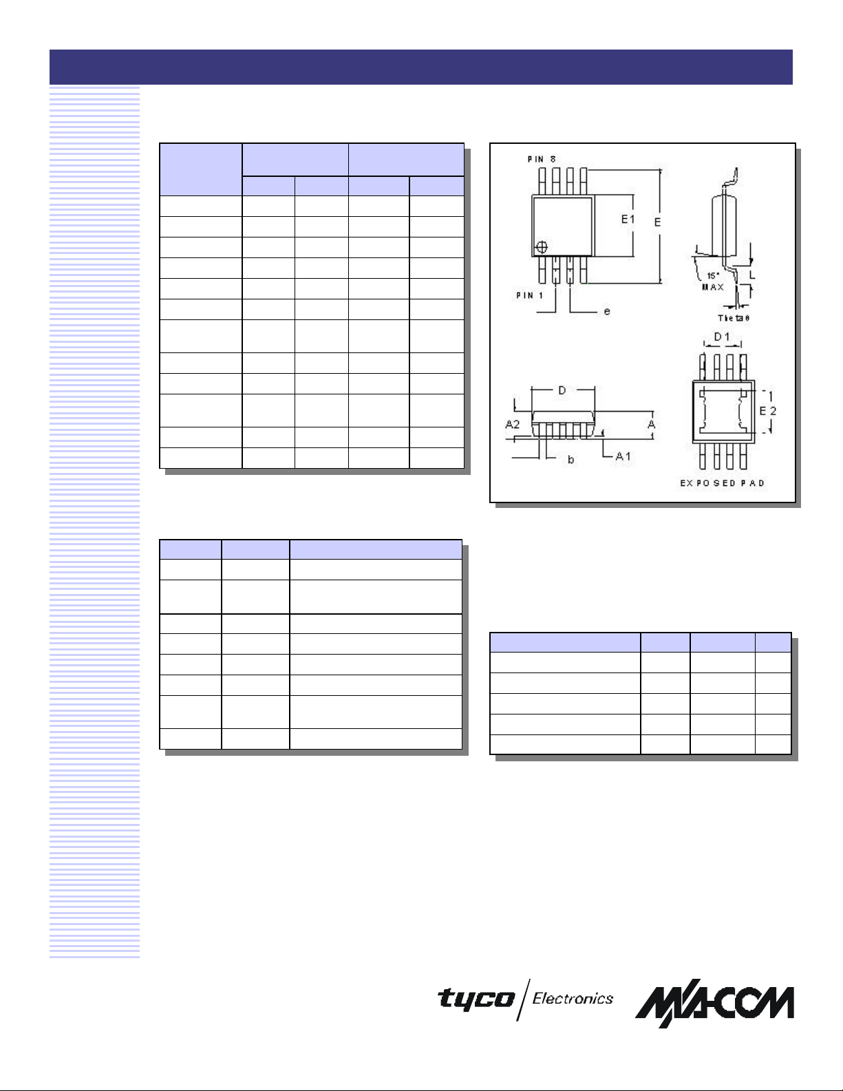
MSOP-8EP Plastic Package
AM52- 0024
V 1.4
Dimensions
A 0.80 1.10 0.0315 0.0433
A1 0.026 0.076 0.0010 0.0030
A2 0.75 0.95 0.0295 0.0374
b 0.25 0.40 0.0098 0.0157
D 2.90 3.10 0.1142 0.01220
D1 1.85 ref. 1.85 ref. 0.073 ref. 0.073 ref.
E 4.90
E1 2.90 3.10 0.1142 0.1220
E2 1.73 ref 1.73 ref. 0.068 ref. 0.068 ref.
e 0.65
L 0.40 1.70 0.0157 0.0276
Theta (θ) 0° 6° 0° 60°
Pin Configuration
Pin
1 VD1 Drain Voltage for First Stage
2 RFIN/VG1 RF input and Gate Voltage for
3 GND Ground
4 VG2 Gate Bias for Second Stage
5 VG3 Gate Bias for Third Stage
6 GND Ground
7 RF
8 VD2 Drain Voltage for Second Stage
Measurement
(mm)
Min Max Min Max
basic
basic
Function Description
OUT/VD3
4.90
basic
0.65
basic
3
RF Output and Drain Voltage for
Measurement
0.1929
basic
0.0256
basic
First Stage
Third Stage
(inches)
0.1929
0.0256
basic
basic
Note: All dimensions per JEDEC MO-187 Var. AA (issue B)
except for D1, E2, and A1. See JEDEC or contact M/A-COM for
additional dimensional and tolerance information.
Absolute Maximum Ratings
Rating
DC Supply Voltage VDD 5.5 V
RF Input Power PIN 10 mW
Junction Temperature TJ 150 °C
Storage Temperature Range T
Operating Temperature T
Symbol Value Unit
-40 to +150 °C
STG
-40 to +100 °C
OPER
4
3. Package bottom is electrical and thermal ground
Specifications subject to change without notice.
n North America: Tel. (800) 366-2266
n Asia/Pacific: Tel.+81-44-844 -8296, Fax +81-44-844-8298
n Europe: Tel. +44 (1344) 869 595, Fax+44 (1344) 300 020
Visit www.macom.com for additional data sheets and product information.
4. Exceeding these limits may cause permanent damage.
2
 Loading...