MACOM AM50-0002SMB, AM50-0002RTR, AM50-0002, AM50-0002TR Datasheet

Low Noise Amplifier
1.575 GHz AM50-0002
V 2.00
F e a t u r e s
●
Low Noise Figure: 1.15 dB
●
High Gain: 27 dB
●
Low Power Consumption: 3 to 5 V, 20 mA
●
High Dynamic Range
●
Low Cost SOIC 8 Plastic Package
D e s c r i p t i o n
M/A-COM's AM50-0002 is a high perf o rmance GaAs
MMIC low noise amplifier in a low cost SOIC 8-lead surface mount plastic package. The AM50-0002 employs a
monolithic 3-stage self-bias design and a simple extern a l
matching network to obtain minimum noise figure. It can
be biased using 3- or 5-volt supplies.
The AM50-0002 is ideally suited for use where low noise
f i g u re, high gain, high dynamic range and low power
consumption are re q u i red. Typical applications include
receiver front ends in the Global Positioning System
(GPS) market, as well as standard gain blocks, buff e r
amps, driver amps and IF amps in both fixed and
portable systems.
M/A-COM's AM50-0002 is fabricated using a mature 0.5m i c ron gate length GaAs process. The process feature s
full passivation for increased perf o rmance re l i a b i l i t y .
Electrical Specifications
TA= +25°C, Z0=50Ω, VDD=+5V, PIN=-35 dBm, f=1.575 GHz
1
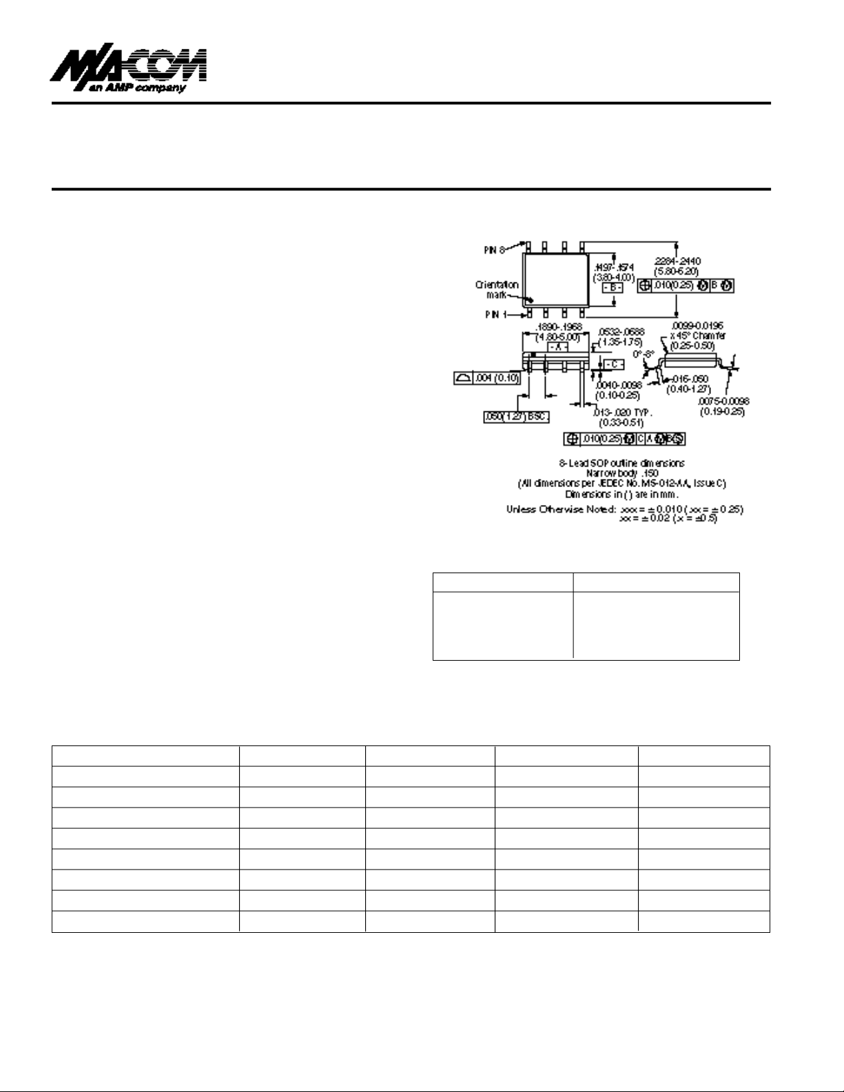
SO-8
Ordering Information
Part Number Package
AM50-0002 SOIC 8-Lead Plastic
AM50-0002TR Forward Tape and Reel*
AM50-0002RTR Reverse Tape and Reel*
AM50-0002SMB Designer’s Kit
If specific reel size is required, consult factory for part number
*
assignment.
Parameter Units Min. Typ. Max.
Gain dB 25 27 29
Noise Figure dB 1.15 1.4
Input VSWR 2.0:1
Output VSWR 1.5:1
Output1 dB Compression dBm 1
Input IP
Reverse Isolation dB 48
Bias Current mA 15 20 25
1. See following pages for 3-volt data.
3
dBm -14

Low Noise Amplifier AM50-0002
Typical Performance
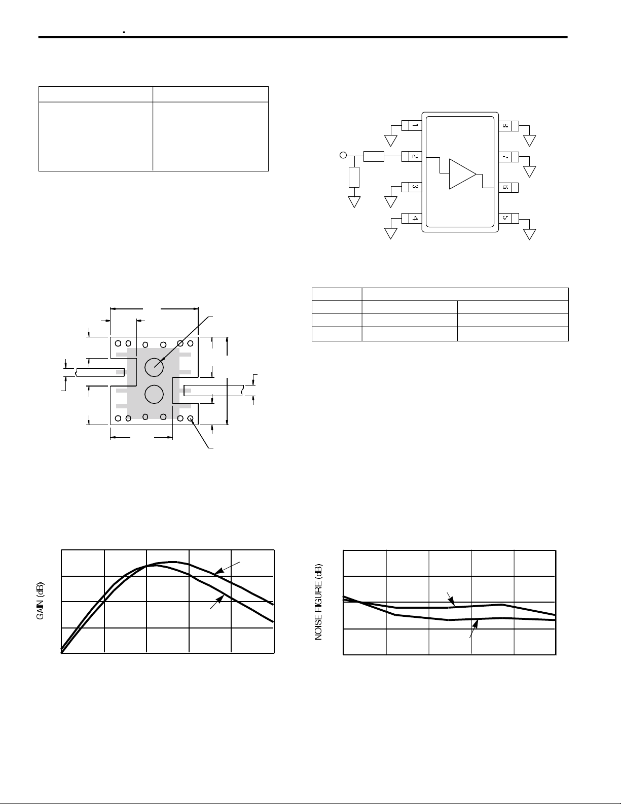
Functional Diagram
Absolute Maximum Ratings
Parameter Absolute Maximum
V
DD
Input Power +17 dBm
Channel Temperature
Operating Temperature -40°C to 85°C
Storage Temperature -65°C to 150°C
2
1
+10 VDC
+150°C
T1
RF IN
GND
GND
GND
V 2.00
1. Operation of this device outside these limits may cause
permanent damage.
2. Typical thermal resistance (ujc) = +165°C/W
Recommended PCB Configuration
Dimensions in inches (mm)
0.244
(6.20)
0.072
(1.83)
0.060
(1.52)
RF IN
0.024
(0.61)
0.109
(2.77)
0.172
(4.37)
FR-4 circuit board, thickness = 0.016 inches (0.41)
2X R 0.025 (0.64)
PLATED THRU
0.112
(2.84)
0.245
(6.22)
RF OUT
0.060
(1.52)
12 X R 0.008 (0.20)
PLATED THRU
0.030
(0.76)
T2
GND
RF OUT, V
GNDGND
Frequency = 1.575 GHz
Impedance Electrical Length
T1 57.2 Ω 36.0°
T2 82.7 Ω 16.2°
3. Pins 1, 3, 4, 5, 7 and 8 must be RF and DC grounded as shown.
4. Pin 2 is the RF input and must be connected to the simple matching
5. Pin 6 is the RF output. VDDis also applied on pin 6.
network shown.
DD
GAIN v s F R E QU E N C Y,TA = +25°C NOISE FIGURE v s F R E QU E N C Y, TA = +25°C
28
26
24
22
20
1.3 1.4 1.5 1.6 1.7 1.8
3 V
FREQUENCY (GHz)
1.4
5 V
1.3
3 V
1.2
1.1
5 V
1.0
1.50 1.52 1.54 1.56 1.58 1.60
FREQUENCY (GHz)
 Loading...