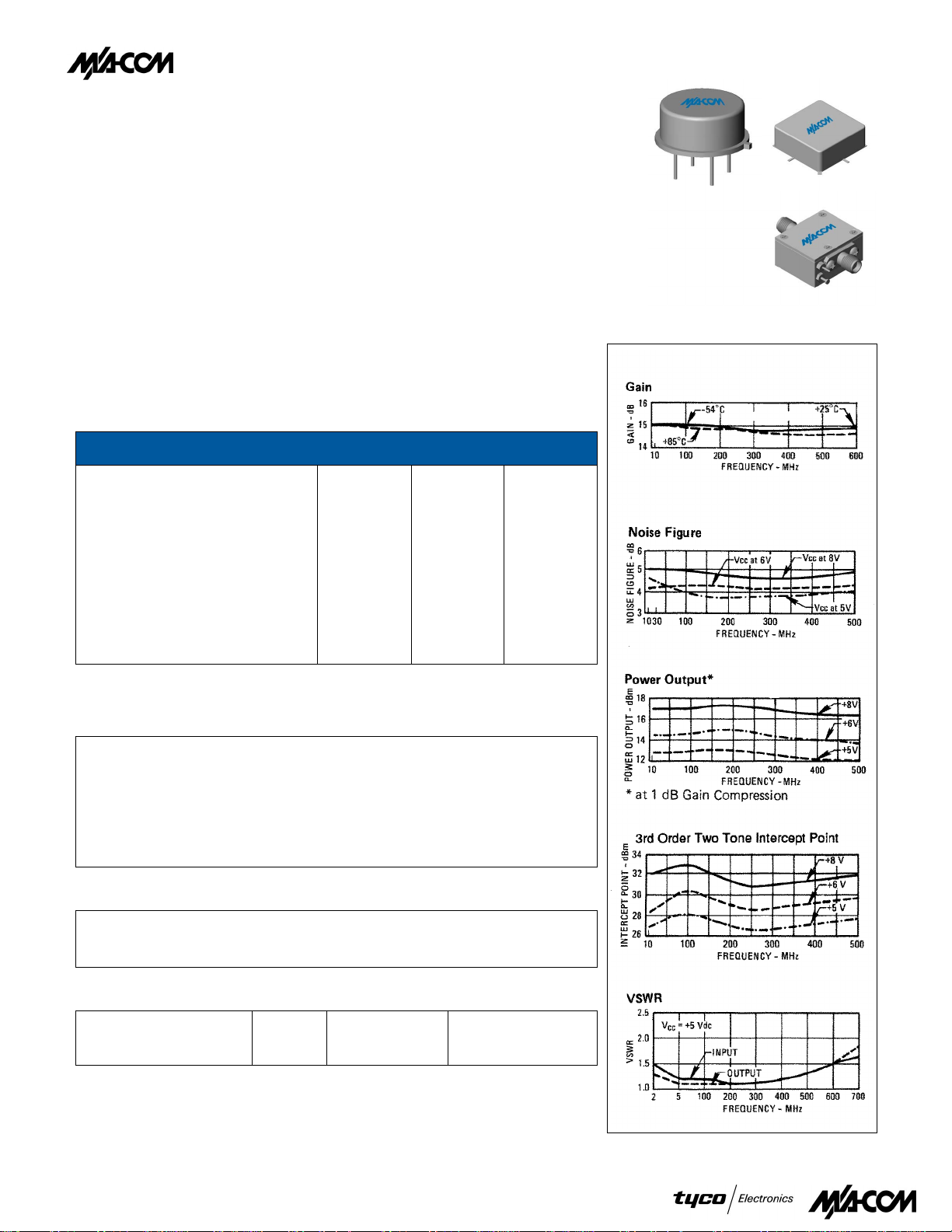
· LOW POWER DRAIN: 31mA (TYP.) @ +5 Vdc
· HIGH OUTPUT LEVEL WITH
LOW Vcc: +12.5 dBm (TYP.) @ 5 Vdc
· HIGH THIRD ORDER I.P.: +28 dBm (TYP.)
@ Vcc = +8 Vdc
A72/SMA72
5 TO 500 MHz
Specifications (Rev. Date: 6/01)*
* Measured in a 50-ohm system at +5 Vdc Nominal. Subject to change without notice.
BG
AA
CE
2-700 MHz
15.0 dB
±0.2 dB
20 dB
3.3 dB
12.5 dBm
+26 dBm
+36 dBm
+42 dBm
1.3:1 / 1.3:1
31 mA
5-500 MHz
14.0 dB
±0.7 dB
11.0 dBm
4.0 dB
11.5 dBm
1.8:1 / 1.8:1
36 mA
1.7:1 / 1.7:1
34 mA
5-500 MHz
13.5 dB
±1.0 dB
4.5 dB
-62° to +125°C
125°C
+9 Volts
+13 dBm
50 mW
0.5 W
125°C
140°C/W
0.126 W
18°C
A72
SMA72
CA72
5 Volts (max.)
5 Vdc
Frequency
Small Signal Gain (min.)
Gain Flatness (max.)
Reverse Isolation
Noise Figure (max.)
Power Output @ 1 dB comp. (min.)
IP3
IP2
Second Order Harmonic IP
VSWR Input / Output (max.)
DC Current @
0
°°°°
to 50
Guaranteed Characteristics Typical
°°°°
C -54
°°°°
to +85
Typical Performance @ 25°C
°°°°
C
Absolute Maximum Ratings
Storage Temperature
Max. Case Temperature
Max. DC Voltage
Max. Continuous RF Input Power
Max. Short Term RF Input Power (1 minute max.)
Max. Peak Power (3 µsec max.)
“S” Series Burn-in Temperature (Case)
Thermal Data: Vcc =
Thermal Resistance
Transistor Power Dissipation P
Junction Temperature Rise Above Case T
θ
jc
d
jc
Outline Drawings
Package TO-8 Surface Mount SMA Connectorized
Figure
Model
Specifications subject to change without notice. • North America: 1-800-366-2266
Visit www.macom.com for complete contact and product information.

WWW.ALLDATASHEET.COM
Copyright ⓒ Each Manufacturing Company.
All Datasheets cannot be modified without permission.
ㅤ
This datasheet has been download from :
www.AllDataSheet.com
ㅤ
100% Free DataSheet Search Site.
Free Download.
No Register.
Fast Search System.
www.AllDataSheet.com
ㅤ
 Loading...