

M/A-Com 19D902797G3, 19D902797G6, 19D902797G7, 19D902797G8, 19D902797G9 Maintenance Manual
...Page 1

Maintenance Manual
450-470 MHz, 110 WATT POWER AMPLIFIER 19D902797G3
403-425 MHz, 90 WATT POWER AMPLIFIER 19D902797G6
425-450 MHz, 90 WATT POWER AMPLIFIER 19D902797G7
380-400 MHz, 75 WATT POWER AMPLIFIER 19D902797G8
470-494 MHz, 90 WATT POWER AMPLIFIER 19D902797G9
492-512 MHz, 90 WATT POWER AMPLIFIER 19D902797G10
410-430 MHz, 90 WATT POWER AMPLIFIER 19D902797G11
TABLE OF CONTENTS
Section Page
1.0 SPECIFICATIONS...................................................................................................................................................3
2.0 DESCRIPTION ........................................................................................................................................................4
3.0 CIRCUIT ANALYSIS..............................................................................................................................................5
3.1 POWER AMPLIFIER ..........................................................................................................................................5
3.1.1 Exciter (U7) ..................................................................................................................................................5
3.1.2 Small Signal Gain Stage ............................................................................................................................... 5
3.1.3 Low Level Amplifier (U1)............................................................................................................................ 5
3.1.4 Driver (Q1) ................................................................................................................................................... 5
3.1.5 Power Amplifier Finals (Q2 & Q3) .............................................................................................................. 6
3.1.6 Low Pass Filter ............................................................................................................................................. 6
3.2 POWER CONTROL ............................................................................................................................................7
3.2.1 Keying and Unkeying the PA .......................................................................................................................7
3.2.2 PA Output Power Set.................................................................................................................................... 7
3.2.3 PA Protection................................................................................................................................................ 7
3.2.4 Theory of Operation......................................................................................................................................7
3.2.5 Signal Interface.............................................................................................................................................8
4.0 TROUBLESHOOTING ......................................................................................................................................... 10
4.1 TROUBLESHOOTING GUIDE ........................................................................................................................ 10
4.2 LOW PASS FILTER TEST PROCEDURE.......................................................................................................13
4.2.1 Recommemded Test Equipment................................................................................................................. 13
4.2.2 Test Set-Up and Procedure .........................................................................................................................13
5.0 PARTS LIST .......................................................................................................................................................... 14
6.0 PRODUCTION CHANGES................................................................................................................................... 23
7.0 IC DATA ................................................................................................................................................................ 26
8.0 ASSEMBLY DIAGRAMS..................................................................................................................................... 29
8.1 POWER AMPLIFIER 19D902797G3 & G6 THROUGH G11..........................................................................29
8.2 COVER ASSEMBLY 19B801659G3 ................................................................................................................ 30
9.0 ASSEMBLY, OUTLINE & SCHEMATIC DIAGRAMS FOR LOW PASS FILTER MODULE 19D902856G331
10.0 OUTLINE DIAGRAM...........................................................................................................................................32
10.1 POWER AMPLIFIER BOARD A1 19D902856G3, G6, G7, G8, G9, G10 & G11........................................... 32
11.0 SCHEMATIC DIAGRAM ..................................................................................................................................... 33
11.1 POWER AMPLIFIER ASSEMBLY 19D902 797G3 & G6 THROUGH G11 ..................................................33
12.0 OUTLINE & SCHEMATIC DIAGRAM FOR 470-512 MHz LOW PASS FILTER MODULE 19D902856G9 . 34
LBI-38674L
Page 2

NOTE
Repairs to this equipment should be made only by an authorized service technician or facility designated by the
supplier. Any repairs, alterations or substitution of recommended parts made by the user to this equipment not
approved by the manufacture could void the user’s authority to operate the equipment in addition to the
manufacture’s warranty.
This manual is published by M/A-COM, Inc., without any warranty. Improvements and changes to this manual necessitated by typographical
errors, inaccuracies of current information, or improvements to programs and/or equipment, may be made by M/A-COM, Inc., at any time
and without notice. Such changes will be incorportated into new editions of this manual. No part of this manual may be reproduced or
transmitted in any form or by any means, electronic or mechanical, including photocopying and recording, for any purpose, without the
express written permission of M/A-COM, Inc.
Copyright© 1992 - 2003 M/A-COM, Inc. All rights reserved.
2 LBI-38674L
Page 3

1.0 SPECIFICATIONS1
ITEM SPECIFICATION
FREQUENCY
OUTPUT POWER (RF)
INPUT POWER (RF)
TEMPERATURE RANGE
SUPPLY VOLTAGE 13.4 Vdc
CURRENT
DUTY CYCLE Continuous
STABILITY
RUGGEDNESS AT HIGH
VSWR
450 MHz - 470 MHz (G3)
403 MHz - 425 MHz (G6)
425 MHz - 450 MHz (G7)
380 MHz - 400 MHz (G8)
470 MHz - 494 MHz (G9)
492 MHz - 512 MHz (G10)
410 MHz - 430 MHz (G11)
65 watts - 130 watts (G3)
55 watts - 110 watts (G6, G7, G9, G10 & G11)
45 watts - 90 watts (G8)
10 mW min. into
-30°C TO +60°C (Ambient air)
29 Amps max. (26 A typical @ rated power, 13.4V) (G3)
29 Amps max. (21 A typical @rated power , 13.4V)(G6, G7, G9, G10 &
G11)
29 Amps max. (20 A typical @ rated power, 13.4V) (G8)
Stable into 3:1 VSWR; all temp.,voltage,freq. 55 watts - 110 watts (G3)
or 45 watts - 90 watts (G6, G7, G9, G10 & G11) or 45 watts - 90 watts
(G8)
No damage into open or shorted load.
≤2:1 VSWR
SPECIFICATIONS
1
These specifications are intended to be used by service personnel during servicing. Refer to the appropriate Specification
Sheet for complete specifications.
LBI-38674L 3
Page 4

DESCRIPTION
2.0 DESCRIPTION
The UHF Power Amplifier Assembly is a wide band RF power amplifier operating over
the 380-400, 410-430, 403-425, 425-450, 450-470, 470-494, and 492-512 MHz range
without tuning. Its main function is to amplify the 10 mW FM signal from the
Transmitter Synthesizer to the rated RF output at the antenna port. The output of the
Power Amplifier Assembly is adjustable from rated power to 3dB lower at the PA output
J104.
The assembly consists of a printed wiring board (A1) and associated components,
including a power module and three RF power transistors, mounted to the heat sink
assembly. The printed wiring board (A1) contains both the power amplifier circuitry and
the power control circuitry.
Unfiltered supply voltage, A+, for the power amplifier circuits enters the assembly via
feedthrough capacitor, C1. Power cable W4 routes the A+ from C1 to J103 on the PWB.
Filtered A+ voltage for the power control circuit enters the assembly via control cable
W13, which connects to the PWB at J201.
The Power Control circuitry sets the output power level by adjusting the PA Power Set
level. It keeps the output power constant despite variations in input power, power
amplifier gain, or temperature through the use of a feedback control loop in the PA
assembly.
4 LBI-38674L
Page 5

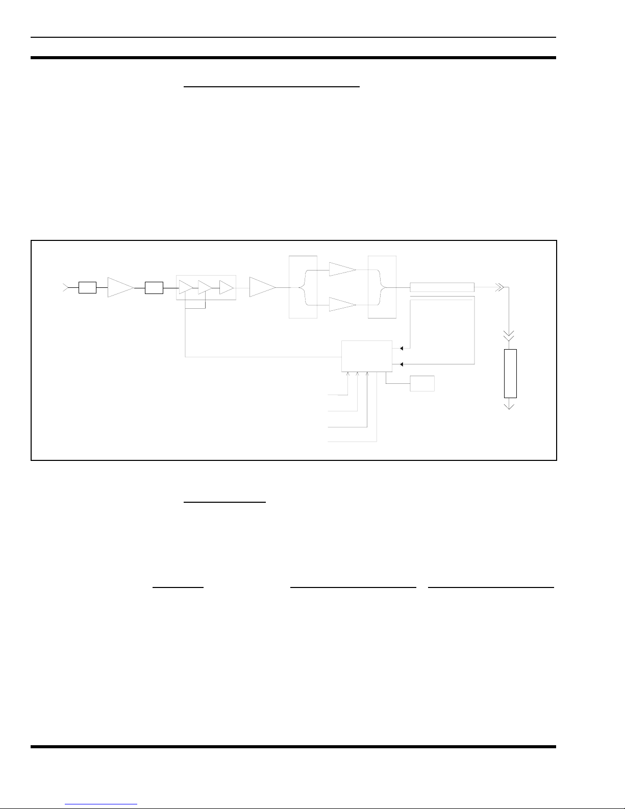
CIRCUIT ANALYSIS
3.0 CIRCUIT ANALYSIS
3.1 POWER AMPLIFIER
The power amplifier section of the PA Board consists of an Exciter, a Small Signal Gain
Stage, a Low Level Amplifier, a Driver, and the Power Amplifier Finals. All these gain
stages have an input and output impedance of 50 ohms. Figure 1 is a block diagram
showing the signal flow within the Power Amplifier Assembly.
3.1.1 Exciter (U7)
The Exciter stage uses a broadband silicon monolithic microwave integrated circuit
(MMIC) amplifier. The signal from transmitter synthesizer, typically 10 dBm (10 mW),
is input to the Exciter through a 10 dB resistive pad (R1, R2, and R31). The Exciter
amplifies the resulting 0 dBm (1 mW) signal to 12 dBm (16 mW).
The MMIC requires a 5 volt supply source. The 8 volt regulator (U100) provides the 5
volts to the MMIC via a dropping resistor R30.
3.1.2 Small Signal Gain Stage
The Small Signal Gain Stage consists of Q7 and its associated bias and matching
circuitry. Collector voltage is fed through R39, R40, and L23. Resistor R33 sets the
quiescent bias of the part. The transistor input impedance is matched to the 50-ohm
output of the Exciter by C59, C61, C62, and L7. L23 and C49 provide the necessary
output matching. The stage provides 14 dB of gain to amplify the signal from the Exciter
to 26 dBm (400 mW).
3.1.3 Low Level Amplifier (U1)
The Low Level Amplifier (LLA) stage uses a 50 ohm thick film RF Power Module to
amplify and control the output power. Internally, the module is a three stage amplifier.
The power control circuitry controls the gain of the first and second stages by varying the
collector voltage level of Q203. The third stage gain remains constant with A+ providing
the DC supply voltage.
The signal from the Small Signal Gain stage, typically 26 dBm (400 mW), is input into
the LLA. Under typical Power Set conditions, the LLA amplifies the signal to a typical
output level of 40.5 dBm (11.2 W).
3.1.4 Driver (Q1)
The driver is a 6 dB RF amplifier consisting of transistor Q1 and its associated circuitry.
The signal from the LLA, typically 40.5 dBm (11.2 W), is amplified to 46.5 dBm (45.0
W). The transistor input is matched to 50 ohms by C65, C66, C27, C67, and a piece of
printed transmission line. The drive signal is then split with a printed in-phase Wilkenson
splitter, providing equal power to each of the final devices.
LBI-38674L 5
Page 6
CIRCUIT ANALYSIS
1
3.1.5 Power Amplifier Finals (Q2 & Q3)
Each of the Power Amplifier final devices is capable of producing 5 to 6 dB of gain. The
output signal from the Splitter is impedance-matched to each of the finals. Under
optimum conditions each final amplifies the input signal to between 50 and 70 watts
output power (depending on band split). The outputs are then impedance-matched to the
input of the Combiner. The Combiner is a printed in-phase Wilkinson type, which
combines (sums) the output power of the finals. This produces an output power of
approximately 100W (depending on band split), which is coupled to the directional
coupler (part of A1 PWB) and on to the antenna circuits. In addition, the directional
coupler samples both forward and reverse power and sends this sample to the Power
Control circuitry
.
PAD
J101
RF IN
10mW
-10 dB
* All power data is per miminum spec. Nominal V oltage (13.4V), 50 Ohm Load,
Room Temperature.
12 dB
GAIN STAGE
16 dB
Q7
SMALL SIGNAL
EXCITER
U1
LOW LEVEL AMPL
3.1.6 Low Pass Filter
Following the Directional Coupler, the RF signal passes through a CHEBYSHEV LC
Low Pass filter (19D902856G3&G9). This passive circuit attenuates any residual
harmonics from the transmit carrier frequency and routes the signal through the RF
output to the antenna. Specifications for this filter are as follows:
Q1
DRIVER
=40W
6 dB
10W
CONTROL VOLTAGE
(4-8V) POWER SET
(2.5-4V) POWER SENSOR
SPLITTER
FILTER A+
PA KEY
=20W
=20W
FINALS
Q2 & Q3
5.0 dB
5.0 dB
Figure 1 - Block Diagram
=60W
=60W
POWER
CONTROL
COMBIMER
DIRECTIONAL
COUPLER
REV FWD
THERMAL
SENSE
J104
RF OUT
130W (G3)
110W (G6, G7, G9, G10 & G1
90W )(G8)
J1
L
P
F
J2
ANTENNA
Parameter
Specifications for Group 3 Specifications for Group 9
Frequency (MHz) 376-470 MHz 470-512 MHz
RF Power Handling (W) 150 Watts 150 Watts
Insertion Loss (dB) 0.4 dB 0.5 dB
Input (VSWR) 1.5:1 Maximum 1.5:1 Maximum
Output (VSWR) 1.5:1 Maximum 1.5:1 Maximum
Harmonic Attenuation (dB) 50 Minimum 760-1500 40 Minimum 940-1024
30 Minimum >1500 MHz 30 Minimum > 1500 MHz
6 LBI-38674L
Page 7
CIRCUIT ANALYSIS
3.2 POWER CONTROL
The Power Control circuitry performs three basic functions. It keys and unkeys the PA,
sets the PA output power, and protects the PA against adverse conditions.
CAUTION
3.2.1 Keying and Unkeying the PA
To key the PA, the digital controller places 5 volts on the PA key line, J201-2. Zero volts
on the PA key line causes the PA to unkey. If the control cable (W13) is disconnected,
with nothing actively driving the PA key line, the PA will remain unkeyed.
3.2.2 PA Output Power Set
PA output power is set according to the level of the Power Set line. Four (4) volts on this
line will produce minimum power. As the voltage increases toward eight (8) volts, the
power will increase to its maximum rated output. The PA output power is initially set at
the factory. This is done by adjusting R43* while injecting a 10 mW signal at J1 and
applying 8 volts to J201-3. After setting the maximum power level, changing the output
power is done by varying the voltage applied on the Power Set line.
*Misadjustment of R43 may result in PA failure.
3.2.3 PA Protection
The Power Control also protects the PA against over temperature and high VSWR
conditions.
An over temperature condition exists when the flange temperature of the final output
transistor reaches 80°C. At this point the output power will drop below its set level. The
output power will continue to drop such that when the flange temperature reaches 125°C
the PA output drops at least 10 dB below its set level.
Reflected power is limited to 25% of the set power. If the output VSWR degrades to
worse than 3:1, the forward power will be reduced to limit the reflected power to 25% of
the set power. The Power Sensor line indicates when the PA is operating in a cutback
condition. If the PA is keyed and the power control is cutting back, the Power Sensor line
will drop to zero (0) volts and the PA alarm light on the station will turn on.
3.2.4 Theory of Operation
Power control of the MASTR® III Power Amplifier is accomplished with a feedback
control loop. The three possible feedback signals are: representation of forward power,
temperature sensitive scaled representation of forward power, or representation of
reflected power. These three signals are input to a diode summing junction which selects
the largest of the three for use as the feedback.
LBI-38674L 7
Page 8

CIRCUIT ANALYSIS
The microstrip directional coupler samples the output power and produces a voltage, Vf,
proportional to the forward output power. The power control compares the forward
voltage, Vf, to a reference voltage at U3. The output of U3 controls the current flow thru
Q5 and the output of Q203. The collector output of Q203 adjusts the control voltage,
Vct1 and Vct2. This control voltage is capable of adjusting the total PA output power
since it provides the first two stages DC supply to the Low Level Amplifier, U1.
During over-temperature operation, a scaled representation of the forward power is
maintained constant by varying the control voltage line. Thermal resistor RT1, sensing an
increase in temperature, causes the output of U3.1 to increase. If the output of U3.1
becomes larger than the other feedback lines, the output of U3.4 will begin to decrease.
This in turn will cause the output of Q203 to decrease reducing the supply voltage to U1.
Since the scaling is a function of temperature, the power is reduced as the temperature
increases.
Under VSWR cutback operation the reverse voltage, Vr, representative of the reflected
output power, is held below a threshold by reducing the control voltage as necessary. If
Vr increases at U3.2 beyond the preset threshold, an increase at U3.4 will result. This
causes a subsequent reduction in the control voltage to U1. Thus the power control circuit
reduces the output power in order to limit the reflected power to 25% of the set power.
3.2.5 Signal Interface
The signal interface to the MASTR III Power Amplifier is supported by a six position
feedthrough connector, J201, with the following pinout:
1. PWR Sensor
2. PA Key
3. PA PWR Set
4. NC
5. Ground
6. Fil A+
3.2.5.1 Pwr Sensor
This line indicates when the PA is experiencing adverse conditions. Under normal
operation, while the PA is keyed, this line will be proportional to forward power.
Minimum power (zero watts) corresponds to 2.5 volts while maximum power
corresponds to 4.5 volts. This voltage is not temperature compensated and no effort is
made to calibrate this signal to an absolute power level. It is intended to provide a relative
indication of forward power and to discriminate between normal and cutback operation.
Zero volts on this line, when the PA is keyed, indicates the forward power is cutback.
This power cutback may be due to high reflected power or may be due to high PA
temperatures. This fault condition may indicate a problem with the PA or may indicate a
system problem external to the Power Amplifier. High VSWR may be due to a poor
antenna and high temperature may be due to a blocked cabinet vent. Zero volts on this
line, when the PA is keyed, does not indicate zero forward power. Zero volts indicates the
PA is protecting itself due to adverse conditions. If the adverse condition, either high
VSWR or high temperature is eliminated, the power will return to normal and the PWR
SENSOR voltage will rise above 2.5 volts.
8 LBI-38674L
Page 9

CIRCUIT ANALYSIS
3.2.5.2 PA Key (Interface Connector pin 2)
This line is used to key and unkey the PA. UNKEY = 0 volt and KEY = 5 volts. The
driver of this line must be capable of supplying 5 volts at 1.0 mA. The appropriate key
sequence requires RF from the transmit synthesizer be input to the PA before the KEY
line is energized.
3.2.5.3 PA PWR Set (Interface Connector pin 3)
This line is used to set the RF Power Output of the PA. Minimum power output equals 4
volts and maximum power output equals 8 volts. The driver of this line must be capable
of supplying 8 volts at 1.0 mA.
3.2.5.4 Fil A+ (Interface Connector pin 6)
This line provides the filtered supply voltage for the Power Control. The driver of this
line must be capable of supplying 13.4 volts ±20% at 100 mA.
LBI-38674L 9
Page 10

TROUBLESHOOTING
4.0 TROUBLESHOOTING
4.1 TROUBLESHOOTING GUIDE
SYMPTOM AREAS TO CHECK INDICATIONS
1. No Power or low Power at
Antenna Port.
2. No power at PA output port
and PA ALARM is OFF.
3. No power at PA output port
and PA ALARM is ON
4. Low power at PA output port
and PA ALRAM is OFF.
5. Low power at PA output port
and PA ALARM is ON.
1. Measure the transmitter output
power before the duplexer or
antenna switch (for simplex
mode).
2. Measure the transmitter output
power before the low pass
filter.
3. Measure the transmitter output
power before the optional
isolator at the PA output port.
Station is in receive mode.
1. No RF input to PA. Check
connection between PA and
TX
2. Check the logic or DC inputs to
the PA from the Interface
Board through J201.
a. J201-2 PA KEY 5volts during transmit
b. J201-3 POWER SET
c. J201-6 13.8 VF
3. Defective PA Replace PA
1. Low RF input to PA from TX
Synthesizer.
2. Check the voltage on J2013(POWER SET).
3. Check the power supply
voltage on the collector of Q1,
Q2 and Q3
4. One of the two final PA
transistors (Q2 or Q3) is
defective.
Check for over temperature
and/or a high VSWR condition
due to a mismatch at the
output port.
The presence of power at this port
is an indication of a defective
duplexer, switch, or cables.
The presence of power at this port
is an indication of a defective filter
or cables.
The presence of power at this port
is an indication of a defective
isolator or cables.
TX Synthesizer should deliver a
minimum of 10 Mw
4 volts to 8 volts (4 volts
represents zero RF power)
13.8 Vdc ±20%
Power should be a minimum of 10
mW (10 dBm).
For minimal output power, this
voltage should be above 7 volts.
Voltage should be minimal 13.4
Vdc.
Replace the defective transistor.
The power control circuit protects
the PA by cutting back the power.
In case of a mismatch, refer to
symptom 1.
10 LBI-38674L
Page 11

TROUBLESHOOTING
Table 1 - UHF Power Amplifier Voltage Chart
PARAMETER
(50 ohm, -30°C to +60°C)
SUPPLY VOLTAGE A+ 13.4 V ±20%
CONTROL VOLTAGE Vct1 0 - 12 V
FORWARD VOLTAGE Vf 3 - 7 V
REVERSE VOLTAGE Vr 2 - 6 V
POWER SENSE J201-1 2.5 - 4 V
PA KEY J201-2 5 V
POWER SET J201-3 4 - 8 V
13.8 VF J201-6 13.8 V ±20%
REFERENCE
SYMBOL
READINGS
(Volts DC)
Table 2 - UHF Power Amplifier Typical Voltage Readings
(50 Ohm, Room Temperature, 13.4 Vdc Supply Voltage, and Rated Output)
Frequency
Group Low Mid High
G3 450 MHz 460 MHz 470 MHz
G6 403 MHz 414 MHz 425 MHz
G7 425 MHz 437 MHz 450 MHz
G8 380 MHz 390 MHz 400 MHz
G9 470 MHz 482 MHz 494 MHz
Vct (Volts DC)
Vf (Volts DC)
G10 492 MHz 502 MHz 512 MHz
G11 410 MHz 420 MHz 430 MHz
G3 7 - 10 Volts 6 - 8 Volts 4 - 6 Volts
G6 6 - 8 Volts 6 - 8 Volts 6 - 8 Volts
G7 6 - 8 Volts 6 - 8 Volts 6 - 8 Volts
G8 6 - 8 Volts 6 - 8 Volts 6 - 8 Volts
G9 & G10 6 - 8 Volts 6 - 8 Volts 6 - 8 Volts
G11 6 - 8 Volts 6 - 8 Volts 6 - 8 Volts
G3 5 - 7 Volts 5 - 7 Volts 5 - 7 Volts
G6 6 - 8 Volts 6 - 8 Volts 6 - 8 Volts
G7 6 - 8 Volts 6 - 8 Volts 6 - 8 Volts
G8 6 - 8 Volts 6 - 8 Volts 6 - 8 Volts
G9 & G10 6 - 8 Volts 6 - 8 Volts 6 - 8 Volts
G11 6 - 8 Volts 6 - 8 Volts 6 - 8 Volts
Continued
LBI-38674L 11
Page 12

TROUBLESHOOTING
Continued
Vr (Volts DC)
J201-1
(Volts DC)
Group Low Mid High
G3 2 - 3 Volts 2 - 3 Volts 2 - 3 Volts
G6 2 - 3 Volts 2 - 3 Volts 2 - 3 Volts
G7 2 - 3 Volts 2 - 3 Volts 2 - 3 Volts
G8 2 - 3 Volts 2 - 3 Volts 2 - 3 Volts
G9 & G10 2 - 3 Volts 2 - 3 Volts 2 - 3 Volts
G11 2 - 3 Volts 2 - 3 Volts 2 - 3 Volts
G3 2.5 - 4 Volts 2.5 - 4 Volts 2.5 - 4 Volts
G6 2.5 - 4 Volts 2.5 - 4 Volts 2.5 - 4 Volts
G7 2.5 - 4 Volts 2.5 - 4 Volts 2.5 - 4 Volts
G8 2.5 - 4 Volts 2.5 - 4 Volts 2.5 - 4 Volts
G9 & G10 2.5 - 4 Volts 2.5 - 4 Volts 2.5 - 4 Volts
G11 2.5 - 4 Volts 2.5 - 4 Volts 2.5 - 4 Volts
J201-3
(Volts DC)
J201-6
(Volts DC)
G3 6 - 8 Volts 6 - 8 Volts 6 - 8 Volts
G6 6 - 8 Volts 6 - 8 Volts 6 - 8 Volts
G7 6 - 8 Volts 6 - 8 Volts 6 - 8 Volts
G8 6 - 8 Volts 6 - 8 Volts 6 - 8 Volts
G9 & G10 6 - 8 Volts 6 - 8 Volts 6 - 8 Volts
G11 6 - 8 Volts 6 - 8 Volts 6 - 8 Volts
G3 13.4 Volts 13.4 Volts 13.4 Volts
G6 13.4 Volts 13.4 Volts 13.4 Volts
G7 13.4 Volts 13.4 Volts 13.4 Volts
G8 13.4 Volts 13.4 Volts 13.4 Volts
G9 & G10 13.4 Volts 13.4 Volts 13.4 Volts
G11 13.4 Volts 13.4 Volts 13.4 Volts
12 LBI-38674L
Page 13

TROUBLESHOOTING
Table 3 - Rated Power For MASTR III UHF Base Station
WITH
FREQUENCY
MHz
450-470 110W 65-130W 75W 100W 70W
425-450 90W 55-110W 60W 82W 55W
403-425 90W 55-110W 60W 82W 55W
380-400 75W 45-90W 50W 68W 47W
410-430 90W 55-110W 60W 82W 55W
470-494 90W 55-110W 60W 82W 55W
492-512 90W 55-110W 60W 82W 55W
STANDARD
@J2
ADJUSTABLE
RANGE@J104
WITH
DUPLEXER
WITH
ISOLATOR
DUPLEXER
AND
ISOLATOR
4.2 LOW PASS FILTER TEST PROCEDURE
This procedure is used to measure Insertion Loss and Harmonic Attenuation of Low Pass
Filters 19D902856G3 and G9. Refer to section 3.1.6 Low Pass Filter for filter
specifications.
4.2.1 Recommemded Test Equipment
Network Analyzer - Similar to HP8753B •
• • Tracking Generator - Similar to HP8444A
Spectrum Analyzer - Similar to HP8567A
4.2.2 Test Set-Up and Procedure
A. Connect two RG400 cables (1ft) with type N connectors on both ends to the
input/output of the filter and to the input/output of the analyzer.
B. Calibrate the analyzer at the end of cables to cover 350-100 MHz for G3 or 450-1200
MHz for G9.
C. Measure Insertion Loss of the filter module at 375, 400, 425, 450 & 475 MHz for G3
or 470, 480, 490, 500 and 515 MHz for G9.
D. Measure Attenuation of the filter module at 750 and 1000 MHz for G3 or 940 and
1024 MHz for G9.
LBI-38674L 13
Page 14

PARTS LIST
5.0 PARTS LIST2
110-WATT UHF POWER AMPLIFIER 19D902797G3
90-WATT UHF POWER AMPLIFIER 19D902797G6, G7 & G9-G11
75-WATT UHF POWER AMPLIFIER 19D902797G8
Issue 8
Symbol Part Number Description
ASSEMBLIES
A1 POWER AMPLIFIER BOARD
- - - - - - - - - - CAPACITORS - - - - - - - - -
C1 19A116708P2
C1 19A702052P26
C2
thru
C9
C10 344A3126P38
C11 19A702061P63
C12 19A705108P40
C13
thru
C16
C17 19A702052P26
C18 19A705108P40
C19 344A3126P38
C20
and
C21
C22
and
C23
C24 19A702061P63
C25 344A3126P38
C26 344A3126P62
C27 344A3126P13
C27 344A3126P15
C28 344A3126P18
C28 344A3126P15
C28 344A3126P13
C28 344A3126P11
C29 344A3126P18
C29 344A3126P15
C29 344A3126P13
19A702061P63
344A3126P38
19A705108P40
19A702052P26
Feedthru: 0.01µF +100-0%, 500 VDCW; sim to Erie 327-050-X5W0103P.
Ceramic: 0.1 µF ±10%, 50 VDCW,
Ceramic: 120 pF ±5%, 50 VDCW, temp coef 0 ±30 PPM.
Porcelain: 100 pF ±5%, 500 VDCW. sim to 101JT500X.
Ceramic: 120 pF ±5%, 50 VDCW, temp coef 0 ±30 PPM.
Mica chip: 120 pF, ±5%, 100 VDCW. temp coef 0 ±50 PPM°C.
Porcelain: 100 pF ±5%, 500 VDCW. sim to 101JT500X.
Ceramic: 0.1 µF ±10%, 50 VDCW.
Mica chip: 120 pF, ±5%, 100 VDCW. temp coef 0 ±50 PPM°C.
Porcelain: 100 pF ±5%, 500 VDCW. sim to 101JT500X.
Mica chip: 120 pF, ±5%, 100 VDCW. temp coef 0 ±50 PPM°C.
Ceramic: 0.1 µF ±10%, 50 VDCW.
Ceramic: 120 pF ±5%, 50 VDCW, temp coef 0 ±30 PPM.
Porcelain: 100 pF ±5%, 500 VDCW. sim to 101JT500X.
Porcelain: 1000 pF ±5%, 500 VDCW; sim to 102JT500X.
Porcelain: 15 pF ±5%, 500 VDCW; sim to 100JT500X. (Used in G7 and
G8).
Porcelain: 12 pF ±5%, 500 VDCW; sim to 120JT500X. (Used in G6 and
G11).
Porcelain: 15 pF ±5%, 500 VDCW; sim to 150JT500X. (Used in G8).
Porcelain: 12 pF ±5%, 500 VDCW; sim to 120JT500X. (Used in G6).
Porcelain: 15 pF ±5%, 500 VDCW; sim to 100JT500X. (Used in G11).
Porcelain: 8.2 pF ±5%, 500 VDCW; sim to 8R2CT500X. (Used in G7).
Porcelain: 15 pF ±5%, 500 VDCW; sim to 150JT500X. (Used in G8).
Porcelain: 12 pF ±5%, 500 VDCW; sim to 120JT500X. (Used in G6).
Porcelain: 15 pF ±5%, 500 VDCW; sim to 100JT500X. (Used in G11).
19D902794G3, G6 - G11
2
COMPONENTS ARE ADDED, DELETED OR CHANGED BY PRODUCTION CHANGES
14 LBI-38674L
Page 15

PARTS LIST
Symbol Part Number Description
C29 344A3126P11
C30 344A3126P15
C30 344A3126P11
C31 344A3126P15
C31 344A3126P11
C32
and
C33
C34
and
C35
C36 344A3126P3
C36 344A3126P5
C37 344A3126P2
C38 19A705205P7
C39 19A705108P40
C40 19A702052P26
C41 344A3126P38
C42
thru
C45
C46
and
C47
C46
and
C47
C48 19A702052P26
C49 19A702236P40
C50 19A702052P26
C51 19A705205P7
C53
and
C54
C57 19A705205P7
C58 344A3126P11
C58 344A3126P15
C58 344A3126P7
C59 19A702061P49
C60 19A702061P65
C61 19A702061P17
C62 19A702236P52
C64 344A3126P38
C65 344A3126P11
344A3126P1
344A3126P18
19A702052P26
344A3126P11
344A3126P13
19A705205P7
Porcelain: 8.2 pF ±5%, 500 VDCW; sim to 8R2CT500X. (Used in G7).
Porcelain: 12 pF ±5%, 500 VDCW; sim to 120JT500X. (Used in G8).
Porcelain: 8.2 pF ±5%, 500 VDCW; sim to 8R2CT500X. (Used in G3, G9,
G10).
Porcelain: 12 pF ±5%, 500 VDCW; sim to 120JT500X. (Used in G8).
Porcelain: 8.2 pF ±5%, 500 VDCW; sim to 8R2CT500X. (Used in G3, G9,
G10).
Porcelain: 3.3 pF ±.25pF, 500 VDCW; sim to 3R3CT500X. (Used in G3).
Porcelain: 15 pF ±5pF, 500 VDCW; simto 150JT500X. (Used in G6, G7
and G11).
Porcelain: 3.9 pF ±0.25%, 500 VDCW; sim to 3R9CT500X. (Used in G8).
Porcelain: 4.7 pF ±0.25%, 500 VDCW; sim to 4R7CT500X. (Used in G6
and G11).
Porcelain: 2.2 pF ±0.25%, 500 VDCW; sim to 2R2CT500X. (Used in G8).
Tantalum: 10 µF, 25 VDCW; sim to Sprague 293D. (Used in G8, G9, G10
and G11).
Mica chip: 120 pF, ±5%, 100 VDCW. temp coef 0 ±50 PPM/°C. (Used in
G8, G9, G10 and G11).
Ceramic: 0.1 µF ±10%, 50 VDCW. (Used in G8, G9 and G10).
Porcelain: 100 pF ±5%, 500 VDCW. sim to 101JT500X. (Used in G11).
Ceramic: 0.1 µF ±10%, 50 VDCW.
Porcelain: 8.2 pF ±5%, 500 VDCW; sim to 8R2CT500X. (Used in G9 and
G10).
Porcelain: 15 pF ±5%, 500 VDCW; sim to 100JT500X. (Used in G10).
Ceramic: 0.1 µF ±10%, 50 VDCW.
Ceramic: 39 pF ±5%, 50 VDCW, temp coef 0 ±30 PPM/°C.
Ceramic: 0.1 µF ±10%, 50 VDCW.
Tantalum: 10 µF, 25 VDCW; sim to Sprague 293D.
Tantalum: 10 µF, 25 VDCW; sim to Sprague 293D.
Tantalum: 10 µF, 25 VDCW; sim to Sprague 293D.
Porcelain: 8.2 pF ±5%, 500 VDCW; sim to 8R2CT500X. (Used in G3).
Porcelain: 12 pF ±5%, 500 VDCW ; sim to 120JT500X. (Used in G6, G7,
G8 and G11).
Porcelain: 5.6 pF ±0.25%, 500 VDCW; sim to 5R6CT500X. (Used in G9,
G10).
Ceramic: 56 pF ±5%, 50 VDCW, temp coef 0 ±30 PPM.
Ceramic: 150 pF ±5%, 50 VDCW, temp coef 0 ±30 PPM/°C.
Ceramic: 12 pF ±10 pF, 50 VDCW, temp coef 0 ±30 PPM/°C.
Ceramic: 120 pF ±5%, 50 VDCW, temp coef 0 ±30 PPM/°C.
Porcelain: 100 pF ±5%, 500 VDCW; sim to 101JT500X.
Porcelain: 8.2 pF ±5%, 500 VDCW; sim to 8R2CT500X. (Used in G3).
LBI-38674L 15
Page 16

PARTS LIST
Symbol Part Number Description
C65 344A3126P5
C66 19A700006P58
C66 19A700006P55
C66 19A700006P50
C66 19A700006P48
C67 19A700006P58
C67 19A700006P50
C67 19A700006P49
C67 19A700006P55
C68 19A700006P58
C68 19A700006P50
C68 19A700006P48
C68
and
C69
C68 19A700006P55
C69 19A700006P49
C69 19A700006P58
C69 19A700006P50
C69 19A700006P55
C69 19A700006P57
C70 19A702061P49
C71 19A702061P63
C72
and
C73
C75
thru
C77
C78
and
C79
C81 344A3126P62
C82
and
C83
C84 19A702061P89
C85
and
C86
C87 19A700006P50
C87 19A700006P60
C87 19A700006P58
C87 19A700006P57
C87 19A700006P55
C88 19A700006P59
C88 19A700006P57
C88 19A700006P48
19A700006P53
19A702052P26
19A702052P26
19A705205P7
19A705108P40
19A705108P40
Porcelain:4.7 pF ±0.25%, 500 VDCW; sim to 4R7CT500X. (Used in G9,
G10).
Mica/teflon: 47 pF ±2%, 100 VDCW. (Used in G8).
Mica/teflon: 27 pF ±2%, 100 VDCW. (Used in G9 and G10).
Mica/teflon: 39 pF ±2%, 100 VDCW. (Used in G6, G7, and G11).
Mica/teflon: 33 pF ±2%, 100 VDCW. (Used in G3).
Mica/teflon: 47 pF ±2%, 100 VDCW. (Used in G6 and G11).
Mica/teflon: 39 pF ±2%, 100 VDCW. (Used in G7 and G8).
Mica/teflon: 36 pF ±2%, 100 VDCW (G3).
Mica/teflon: 27 pF ±2%, 100 VDCW. (Used in G9 and G10).
Mica/teflon: 47 pF ±2%, 100 VDCW. (Used in G8 and G11).
Mica/teflon: 39 pF ±2%, 100 VDCW. (Used in G6, G7, and G11).
Mica/teflon: 33 pF ±2%, 100 VDCW (G3).
Mica/teflon: 22 pF ±2%, 100 VDCW. (Used in G10).
Mica/teflon: 27 pF ±2%, 100 VDCW. (Used in G9).
Mica/teflon: 36 pF ±2%, 100 VDCW (G3).
Mica/teflon: 47 pF ±2%, 100 VDCW. (Used in G6 and G11).
Mica/teflon: 39 pF ±2%, 100 VDCW (G7).
Mica/teflon: 27 pF ±2%, 100 VDCW. (Used in G9).
Mica/teflon: 43 pF ±2%, 100 VDCW. (Used in G8).
Ceramic: 56 pF ±5%, 50 VDCW, temp coef 0 ±30 PPM.
Ceramic: 120 pF ±5%, 50 VDCW, temp coef 0 ±30 PPM.
Ceramic: 0.1 µF ±10%, 50 VDCW.
Ceramic: 0.1 µF ±10%, 50 VDCW.
Tantalum: 10 µF, 25 VDCW; sim to Sprague 293D.
Porcelain: 1000 pF ±5%, 500 VDCW; sim to 102JT500X.
Mica chip: 120 pF, ±5%, 100 VDCW, temp coef 0 ±50 PPM/°C.
Ceramic: 1500 pF ±5%, 50 VDCW, temp coef 0 ±30 PPM.(Used in G3, G6G9, G11).
Mica chip: 120 pF, ±5%, 100 VDCW, temp coef 0 ±50 PPM/°C.
Mica/teflon: 39 pF ±2%, 100 VDCW. (Used in G3).
Mica/teflon: 56 pF ±2%, 100 VDCW. (Used in G8).
Mica/teflon: 47 pF ±2%, 100 VDCW. (Used in G6, and G11).
Mica/teflon: 43 pF ±2%, 100 VDCW. (Used in G7).
Mica/teflon: 27 pF ±2%, 100 VDCW (Used in G9 & G10).
Mica/teflon: 51 pF ±2%, 100 VDCW. (Used in G6, G8, and G11).
Mica/teflon: 43 pF ±2%, 100 VDCW. (Used in G7).
Mica/teflon: 33 pF ±2%, 100 VDCW. (Used in G3).
16 LBI-38674L
Page 17

PARTS LIST
Symbol Part Number Description
C88 19A700006P48
C89 19A700006P59
C89 19A700006P57
C89 19A700006P50
C89 19A700006P48
C90 19A700006P48
C90 19A700006P60
C90 19A700006P58
C90 19A700006P57
C90 19A700006P55
C91 19A700006P57
C91 19A700006P58
C91 19A700006P49
C91 19A700006P48
C92 19A700006P59 Mica/teflon:(Used in G8).
C92 19A700006P57
C92 19A700006P50
C92 19A700006P48
C92 19A700006P55
C93 19A700006P59
C93 19A700006P57
C93 19A700006P50
C93 19A700006P48
C93 19A700006P55
C94 19A700006P57
C94 19A700006P49
C94 19A700006P58
C94 19A700006P48
- - - - - - - - - - - - DIODES - - - - - - - - - - - -
D1
thru
D3
D4
thru
D6
- - - - - - - - - - - - - - JACKS - - - - - - - - - - - - - -
J101 19A705512P1 Connector, RF SMB Series: sim to AMP No. 221111-1.
J103 19A134263P1 Contact, electrical: sim to Selectro 229-1082-00-0-590.
J104 7777145P5 Receptacle: sim to Amphenol 82-97.
J201 19A704852P32 Printed wire, two part: 6 contact: sim to Molex 22-29-2061.
- - - - - - - - - - - - - - INDUCTORS - - - - - - - - - - - - - -
L1 19C320617P10 Coil.(Used in G3, G6-G9 and G11).
L1 19C320617P17 Coil.(Used in G10).
L2 19A701091G1 Coil (Used in G6, G7, G8 and G11).
L3 19C320617P10 Coil (Used in G6, G7, G8, G10 and G11).
L4 19C320617P28 Coil.
19A705377P4 Silicon: Hot Carrier; sim to HP HSMS-2802.
19A700053P3 Silicon: 2 Diodes in Series, Common Cathode; sim to MBAV70L.
Mica/teflon: 33 pF ±2%, 100 VDCW. (Used in G9 and G10).
Mica/teflon: 51 ohms ±2%, 100 VDCW. (Used in G6, G8, and G11).
Mica/teflon: 43 pF ±2%, 100 VDCW. (Used in G7).
Mica/teflon: 39 pF ±2%, 100 VDCW. (Used in G3).
Mica/teflon: 33 pF ±2%, 100 VDCW. (Used in G9 and G10).
Mica/teflon: 33 pF ±2%, 100 VDCW. (Used in G3).
Mica/teflon: 56 pF ±2%, 100 VDCW. (Used in G8).
Mica/teflon: 47 pF ±2%, 100 VDCW. (Used in G6 and G11).
Mica/teflon: 43 pF ±2%, 100 VDCW. (Used in G7).
Mica/teflon: 27 pF ±2%, 100 VDCW (Used in G9 & G10).
Mica/teflon: 43 pF ±2%, 100 VDCW. (Used in G8).
Mica/teflon: 47 pF ±2%, 100 VDCW. (Used in G9 and G11).
Mica/teflon: 36 pF ±2%, 100 VDCW. (Used in G7).
Mica/teflon: 33 pF ±2%, 100 VDCW. (Used in G3, G9 and G10).
Mica/teflon: 43 pF ±2%, 100 VDCW. (Used in G6 and G11).
Mica/teflon: 39 pF ±2%, 100 VDCW. (Used in G7).
Mica/teflon: 33 pF ±2%, 100 VDCW. (Used in G3).
Mica/teflon: 27 pF ±2%, 100 VDCW. (Used in G9 and G10).
Mica/teflon: 51 ohms ±2%, 100 VDCW. (Used in G8).
Mica/teflon: 43 pF ±2%, 100 VDCW. (Used in G6 and G11).
Mica/teflon: 39 pF ±2%, 100 VDCW. (Used in G7).
Mica/teflon: 33 pF ±2%, 100 VDCW. (Used in G3).
Mica/teflon: 27 pF ±2%, 100 VDCW. (Used in G9 and G10).
Mica/teflon: 43 pF ±2%, 100 VDCW. (Used in G8).
Mica/teflon: 36 pF ±2%, 100 VDCW (G7).
Mica/teflon: 47 pF ±2%, 100 VDCW. (Used in G6 and G11).
Mica/teflon: 33 pF ±2%, 100 VDCW. (Used in G3, G9, and G10).
LBI-38674L 17
Page 18

PARTS LIST
Symbol Part Number Description
L5 19A701091G1 Coil (Used in G6, G7, G8 and G11).
L6 19C320617P10 Coil (Used in G6, G7, G8, G10 and G11).
L7 19A705470P4 Coil, Fixed: 15 nH; sim to Toko 380NB-15nM.
L8 19A705470P8 Coil, Fixed: 39 nH; sim to Toko 380NB-39nM.
L14 19C320617P17 Coil.
L15
thru
L17
L18 19C320617P17 Coil.
L23 19A705470P8 Coil, Fixed: 39 nH; sim to Toko 380NB-39nM.
L25 19A701091G1 Coil.
L29
and
L30
- - - - - - - - - - - TRANSISTORS - - - - - - - - - - - -
Q1 344A3948P1 Silicon, NPN: 440-512 MHz, 50W; sim to MRF 650.
Q2
and
Q3
Q4
and
Q5
Q7 344A3058P1 Silicon, NPN
Q203 19A700055P1 Silicon, PNP.
- - - - - - - - - - - - RESISTORS - - - - - - - - - - - -
R1
and
R2
R3
thru
R6
R7 19B800607P183
R8
thru
R10
R11 19B800607P223
R12
thru
R18
R19
and
R20
R21
thru
R23
R24
thru
R26
R27 19B800607P822
R28
and
R29
R30 19B800607P750
R31 19B800607P470
19A700024P13
19C320617P10 Coil.
344A4134P1 Silicon, NPN: 470-512 MHz, 65W; sim to MRF 658.
19A700076P2 Silicon, NPN: sim to MMBT3904, low profile.
19B800607P220
19B801486P101
19B800607P103
19B800607P103
19B800607P472
19B800607P102
19B800607P103
19A143832P6
Coil, RF: 1.0 µH ±20%.
Metal film: 22 ohms ±5%, 1/8 w.
Metal film: 100 ohms ±5%, 1/2 w.
Metal film: 18K ohms ±5%, 1/8 w.
Metal film: 10K ohms ±5%, 1/8 w.
Metal film: 22K ohms ±5%, 1/8 w.
Metal film: 10K ohms ±5%, 1/8 w.
Metal film: 4.7K ohms ±5%, 1/8 w.
Metal film: 1K ohms ±5%, 1/8 w.
Metal film: 10K ohms ±5%, 1/8 w.
Metal film: 8.2K ohms ±5%, 1/8 w.
Power: 100 ohms ±5%, 40 w.
Metal film: 75 ohms ±5%, 1/8w.
Metal film: 47 ohms ±5%, 1/8 w.
18 LBI-38674L
Page 19

PARTS LIST
Symbol Part Number Description
R32 19A700050P17
R33 19B800607P682
R34 19B801486P100
R35 19A700050P17
R36 19B801486P101
R37 19B801486P331
R38 19B800607P223
R39
and
R40
R41 19A702931P333
R42 19A702931P293
R43 19A700109P5
R44
thru
R46
R47
and
R48
R49 19B801486P101
R50 19B800607P1 Metal film: Jumper. (Used in G8, G9, G10 and G11).
R51 19B801486P331
R52 19B801486P100
R53 19B800607P1 Metal film: Jumper.
R54 19B800607P472
R55 19B800607P103
R56 19B800607P330
R57 19B800607P222
R58
and
R59
- - - - - - - - - - - - - - THERMISTOR - - - - - - - - - - - - - -
RT1 19A705813P2 Thermistor: sim to AL03006-58.2K-97-G100.
- - - - - - - - - - - VOLTAGE REGULATORS - - - - - - - - - - -
VR1
and
VR2
- - - - - - - - - - - - - - CAPACITORS - - - - - - - - - - - - - -
C1 19A116708P2
- - - - - - - - - - - - - - JACKS - - - - - - - - - - - - - -
J1 Part of W1.
J104 7777145P5 Receptacle: sim to Amphenol 82-97.
- - - - - - - - - - - - - - TRANSISTORS - - - - - - - - - - - - - -
Q1 344A3948P1 Silicon, NPN: UHF Amplifier; sim to Motorola MRF 650.
Q2
and
Q3
Q203 19A700055P1 Silicon, PNP: Darlington; sim to TIP-125.
19B800607P100
19B801486P101
19B801486P750
19A700113P7
19A700083P102 Silicon: 5.1 Volt Zener; sim to BZX84-C5V1.
344A4134P1 Silicon, NPN: UHF Amplifier.
Wirewound: 2.2 ohms ±10%, 2 w. (Used in G3, G9, and G10).
Metal film: 6.8K ohms ±5%, 1/8 w.
Metal film: 10 ohms ±5%, 1/2 w.
Wirewound: 2.2 ohms ±10%, 2 w. (Used in G3, G9).
Metal film: 100 ohms ±5%, 1/2 w. (Used in G40, G3, and G6).
Metal film: 330 ohms ±5%, 1/2 w. (Used in G3, G6-G9, G11).
Metal film: 22K ohms ±5%, 1/8 w.
Metal film: 10 ohms ±5%, 1/8 w.
Metal film: 21.5K ohms ±1%, 200 VDCW, 1/8 w.
Metal film: 9090 ohms ±1%, 200 VDCW, 1/8 w.
Variable, cermet: 25 ohms to 10K ohms ±20%, 1/4 w.
Metal film: 100 ohms ±5%, 1/2 w.
Metal film: 75 ohms ±5%, 1/2 w.
Metal film: 100 ohms ±5%, 1/2 w. (Used in G3, G6-G9, G11).
Metal film: 330 ohms ±5%, 1/2 w.(Used in G3, G6-G9, G11).
Metal film: 10 ohms ±5%, 1/2 w.
Metal film: 4.7 ohms ±5%, 1/8 w.
Metal film: 10K ohms ±5%, 1/8 w.
Metal film: 33 ohms ±5%, 1/8 w.
Metal film: 2.2 ohms ±5%, 1/8 w.
Composition: 4.7 ohms ±5%, 1/2 w (Used in G10).
Ceramic feedthru: 0.01 µF -0 +100%, 500 VDCW; sim to Erie 327-050X5W0103P.
LBI-38674L 19
Page 20

PARTS LIST
Symbol Part Number Description
- - - - - - - - - - - - - - RESISTORS - - - - - - - - - - - - - -
R28
and
R29
- - - - - - - - - - -INTEGRATED CIRCUITS - - - - - - - - - - - -
U1 19A705457P2 PA module: 440-470 MHz; sim to M57704H. (Used in G3).
U1 19A705457P1 PA module: 400-450 MHz; sim to M57704M. (Used in G7).
U1 19A705457P3 PA module: 470-512 MHz; sim to M57704SH. (Used in G9 and G10).
U1 19A705457P7 PA module: 380-400 MHz; sim to M57704UL. (Used in G8).
U1 19A705457P4 PA module: 400-420 MHz; sim to M57704L. (Used in G6).
U2 19A702293P3 Linear: Dual Op Amp; sim to LM358D.
U3 19A701789P4 Linear: Quad Op Amp; sim to LM224D.
U7 344A3907P1 Monolithic microwave IC (MMIC): sim to Avantek MSA-1105.
U100 19A705532P2 Integrated Circuit, Linear (Positive Voltage Regulator): sim to MC78T15CT.
- - - - - - - - - - - - - - - - CABLES - - - - - - - - - - - - - - - -
W1 19B801529G4 RF Input Cable. Includes the following:
19B800560P2 RF Cable.
19A705512P3 Connector, RF SMB series: sim to AMP 228213-1.
19A115938P1 Connector, coaxial: (BNC Series); sim to Amphenol 31-318.
W4 19B801695G11 Power Cable. Includes the following:
19B209268P115 Solderless terminal.
19B209260P11 Solderless terminal.
19A115959P2 Wire, stranded.
19A701503P2 Cable: battery, red.
19A701503P10 Cable: battery, black.
19B209268P116 Solderless terminal.
W10 19B801937P1 Power cable.
W13 19B801739P1 Power control cable.
- - - - - - - - - - - - - MISCELLANEOUS - - - - - - - - - - - -
2 19D902420P6 Heatsink.
5 19A702381P510 Screw, thread forming: TORX DRIVE No. M3.5 0.6 x 10.
6 7139898P3 Nut, hex, brass: No. 1/4-28.
11 19A702364P310 Machine screw, TORX Drive: No. M3-0.5 x 10.
14 19B209268P113 Terminal, solderless: sim to AMP 2-34835-4. (Used in G11).
19A115959P2 Wire, stranded. (Used in G11).
19B209268P116 Solderless terminal. (Used in G11).
15 7147306P2 Insulator.
16 19A700136P7 Insulated sleeving.
21 19A701863P27 Clip, loop.
22 19A701312P5 Flatwasher: M3.5.
28 19A702364P316 Machine Screw: Pan Head, Steel.
29 19A700034P4 Nut, hex: No. M3 x 0.5MM.
30 19A700033P5 Lock washer, external tooth: No. 3.
35 19A705469P1 Insulator Plate, TO-220.
36 19A700068P1 Insulator, bushing.
37 19A134455P3 Flat washer.
38 19B801659G3 Cover (see separate parts list).
19A143832P6
Power: 100 ohm ±5%, 40 w.
20 LBI-38674L
Page 21

PARTS LIST
Symbol Part Number Description
41 19A700033P6 Loackwasher, external tooth, M3.5.
45 N405P5B6 Lockwasher.
46 19A701312P4 Flatwasher: 3.2 ID.
50 19A702381P408 Tap screw, TORX Drive, M3-0.5 x 8.
51 19A705106P1 Resistor Spacer.
COVER
2 19D902421P1 Power Amplifier Cover.
4 19A702381P522 Screw, thread forming:
5 19A701365P4 Washer.
11 19A149969P3 Shield.
13 5493477P9 Axial fan.
14 5493477P10 Grille.
15 N80P13028B6 Machine screw.
LOW PASS FILTER MODULE3
19D902856G3 & G9
Issue 2
19B801659G3
Symbol Part Number Description
16 N210P21B6 Machine nut.
17 19A701312P5 Flatwasher: M3.5
18 19A701863P10 Clip, loop.
20 19A702364P410 Machine screw.
24 N405P37B6 Lock washer.
25 L401P23B6 Split washer.
26 19A700034P5 Hex nut.
- - - - - - - JACKS - - - - - -
J1
and
J2
- - - - - - MISCELLANEOUS - - - - - -
2 19D903063P1 Casting.
3 119D903064P1 Casting.
5 19A702381P513 Screw, thread forming: TORX, No. M3.5 – 0.6 X 13.
6 19A702364P210 Machine screw, metric: M2.5-0.45 X 10.
7 19A134455P3 Flatwasher.
8 19A700032P3 Lockwasher, tooth, steel, metric: 2.5.
UHF FILTER BOARD
- - - - - - CAPACITORS - - - - - -
C1
thru
C3
C4 19A700006P1 Mica: 4.7 pF ±10%, 100 VDCW.
C5 19A700006P2 Mica: 5.6 pF ±10%, 100 VDCW; sim to Underwood 3HS0020
7777145P5 Receptacle: sim to Amphenol 82-97.
19D902853G3
19A700006P2 Mica: 5.6 pF ±10%, 100 VDCW; sim to Underwood 3HS0020.
3
COMPONENTS ARE ADDED, DELETED OR CHANGED BY PRODUCTION CHANGES
LBI-38674L 21
Page 22

PARTS LIST
Symbol Part Number Description
- - - - - - INDUCTORS - - - - - -
L1
and
L2
L3
thru
L6
UHF FILTER BOARD
- - - - - - - - - - - - CAPACITORS - - - - - - - - - - - -
C1 19A700006P1
C2
and
C3
- - - - - - INDUCTORS - - - - - -
L1
thru
L4
- - - - - - MISCELLANEOUS - - - - - -
11 19A702455P5 Nut, self clinching.
19C320618P7 Coil.
19B227929P1 Coil
Mica: 4.7 pF ±10%, 100 VDCW.
19A700006P3
19C32061P17 Coil.
Mica: 6.8 pF ±10%, 100VDCW.
19D902853G9
22 LBI-38674L
Page 23

PRODUCTION CHANGES
6.0 PRODUCTION CHANGES
Changes in the equipment to improve performance or to simplify circuits are
identified by a "Revision Letter" which is stamped after the model number of the
unit. The revision stamped on the unit includes all previous revisions. Refer to the
Parts List for the descriptions of parts affected by these revisions.
REV. A - POWER AMPLIFIER 19D902797G3
REV. A - POWER AMPLIFIER BOARD 19D902794G3
To make unit ETS compliant.
Changed capacitors C17, C44 & C45. Capacitors C17, C44 & C45 were 19A702052P33.
Changed capacitor C50. Capacitor C50 was 0.068 µF (19A702052P24).
Changed capacitor C61. Capacitor C61 was 8.2 pF (19A702061P12).
Changed capacitor C62. Capacitor C62 was 27 pF (19A702061P33).
Changed capacitor C84. Capacitor C84 was 1000 pF (19A705108P40).
Changed diodes D1, D2 & D3. Diodes D1, D2 & D3 were (19A700047P3)
Changed inductors L15 thru L17. Inductors L15 thru L17 were (19A700024P37).
Changed inductor L24. Inductor L24 was 15nH (19A705470P3).
Changed resistor R33. Resistor R33 was 5.6K (19B800607P562).
Changed resistor R34. Resistor R34 was 3.9 ohms composition (19A700113P5).
Changed transistor Q7. Transistor Q7 was 19A701940P1.
Deleted inductors L26 and L27.
Deleted capacitors C48, C49, C63 & C74.
Added capacitors C1, C25 & C26.
Added resistors R37, R51 & R52
Added RT1.
Added VR2.
REV. B - POWER AMPLIFIER 19D902797G3
REV. B - POWER AMPLIFIER BOARD 19D902794G3
To update PWB for new split.
Changed PWB.
Changed capacitor C26. Capacitor C26 was 100 pF (344A3126P38).
Changed capacitor C81. Capacitor C81 was 100 pF (344A3126P38).
Added capacitors C27 thru C29 and C34 and C35.
Changed resistor R36. Resistor R36 was 150 ohms (19B801486P151).
Changed resistors R44 thru R46. Resistors R44 thru R46 were 150 ohm
(19B801486P151).
Changed resistorsR47 and R48. Resistors R47 and R48 were 39 ohm
(19B801486P390).
Added resistors R32 and R35.
REV. C - POWER AMPLIFIER 19D902797G3
REV. C - POWER AMPLIFIER BOARD 19D902794G3
To update PWB for new band splits.
REV. D - POWER AMPLIFIER 19D902797G3
REV. D - POWER AMPLIFIER BOARD 19D902794G3
To update PWB for new band splits and add power monitor circuitry.
Added dual operational amplifier U2.
Added capacitor C48.
Added resistors R54, R53, R55.
REV. A - POWER AMPLIFIER 19D902797G6
To update PWB to new band splits.
LBI-38674L 23
Page 24

PRODUCTION CHANGES
REV. A - POWER AMPLIFIER 19D902797G7
REV. A - POWER AMPLIFIER BOARD 19D902794G7
To update PWB to new band splits and add power monitor circuitry.
Added dual operational amplifier U2
Added capacitor C48.
Added resistors R54, R53, R55.
REV. A - POWER AMPLIFIER 19D902797G8, G9, G11
REV. A - POWER AMPLIFIER BOARD 19D902794G8, G9, G11
REV. B - POWER AMPLIFIER 19D902797G6, G7
REV. B - POWER AMPLIFIER BOARD 19D902794G6, G7
REV. E - POWER AMPLIFIER 19D902797G3
REV. E - POWER AMPLIFIER BOARD 19D902794G3
To update PWB to new band splits for 492-512 MHz.
REV. F - POWER AMPLIFIER BOARD 19D902794G3
To improve the collector match of the final stage at the upper end of the frequency range
(450-470 MHz). Changed capacitors C88 and C90 from 39 pF to 33 pF. Capacitors C88
and C90 was 19A70006P48.
In TABLE 1 of the Schematic Diagram, under 450-470 MHz
Changed capacitors C88 and C90 from 39 pF to 33 pF.
REV. B - POWER AMPLIFIER 19D902797G11
To improve reliability.
Changed capacitor C67. Capacitor C67 was 39 pF (19A700006P50).
REV. A - POWER AMPLIFIER 19D902797G10
REV. A - POWER AMPLIFIER BOARD 19D902794G10
To improve the collector match of the final stage at the upper end of the frequency range.
Changed capacitors C87 and C90. Capacitors C87 and C90 were 33.0 pF
(19A700006P48).
REV. B - POWER AMPLIFIER BOARD 19D902794G10
To improve the total current drain in the UHF 492 to 512 MHz split. Changed capacitors
in the PA section as follows:
In TABLE 1 of the Schematic Diagram, under 492-512 MHz
Changed capacitor C30 from 8.2 pF to "not used".
Changed capacitor C31 from 8.2 pF to "not used".
Changed capacitor C34 from "not used" to "8.2 pF".
Changed capacitor C35 from "not used" to "8.2 pF".
REV. F - POWER AMPLIFIER 19D902797G3
REV. F - POWER AMPLIFIER 19D902797G6
REV. F - POWER AMPLIFIER 19D902797G7
REV. F - POWER AMPLIFIER 19D902797G8
REV. F - POWER AMPLIFIER 19D902797G9
REV. F - POWER AMPLIFIER 19D902797G10
REV. F - POWER AMPLIFIER 19D902797G11
To identify UHF Power Amplifiers built using solder with 2% silver for everything but
collector leads and solder type NTA 335 48/1 for all collector leads.
REV. G - POWER AMPLIFIER 19D902797G3
REV. G - POWER AMPLIFIER 19D902797G6
REV. G - POWER AMPLIFIER 19D902797G7
REV. G - POWER AMPLIFIER 19D902797G8
24 LBI-38674L
Page 25

PRODUCTION CHANGES
REV. G - POWER AMPLIFIER 19D902797G9
REV. G - POWER AMPLIFIER 19D902797G10
REV. G - POWER AMPLIFIER 19D902797G11
REV. G - POWER AMPLIFIER BOARD 19D902794G3
REV. C - POWER AMPLIFIER BOARD 19D902794G6
REV. C - POWER AMPLIFIER BOARD 19D902794G7
REV. C - POWER AMPLIFIER BOARD 19D902794G8
REV. B - POWER AMPLIFIER BOARD 19D902794G9
REV. C - POWER AMPLIFIER BOARD 19D902794G10
REV. C - POWER AMPLIFIER BOARD 19D902794G11
To improve reliability by making transistor Q7 run cooler when in the PA is in standby.
Changed resistor R1 from 27 ohms to 22 ohms. Resistor R1 was 19B800607P270.
Changed resistor R2 from 27 ohms to 22 ohms. Resistor R2 was 19B800607P270.
Changed resistor R31 from 33 ohms to 47 ohms. Resistor R31 was 19B800607P330
Changed resistor R32 from 3.9K ohms to 6.8K ohms. Resistor R32 was
19B800607P392.
LBI-38674L 25
Page 26

IC DATA
7.0 IC DATA
U1
19A705457P1, P2 AND P4
PA Amplifier Module
U100
19A705532P2
Voltage Regulator
U3
19A701789P4
Quad Op-Amp
26 LBI-38674L
Page 27

IC DATA
U7
MMIC Amplifier
344A3907P1
LBI-38674L 27
Page 28

(Intentionally Left Blank)
28 LBI-38674L
Page 29

ASSEMBLY DIAGRAM
8.0 ASSEMBLY DIAGRAMS
8.1 POWER AMPLIFIER 19D902797G3 & G6 THROUGH G11
(19D902797, Sh. 3, Rev. 16)
LBI-38674L 29
Page 30

ASSEMBLY DIAGRAM
8.2 COVER ASSEMBLY 19B801659G3
(19B801659, Sh. 2, Rev. 3)
(19D902797, Sh. 2, Rev. 16)
30 LBI-38674
L
Page 31

ASSEMBLY, OUTLINE & SCHEMATIC DIAGRAM
9.0 ASSEMBLY, OUTLINE & SCHEMATIC DIAGRAMS FOR
LOW PASS FILTER MODULE 19D902856G3
COMPONENT SIDE
(19D902853, Sh. 2, Rev
(19D902856, Sh. 1, Rev. 1)
(19D903623, Sh. 1, Rev. 1)
LBI-38674L 31
Page 32

OUTLINE DIAGRAM
10.0 OUTLINE DIAGRAM
10.1 POWER AMPLIFIER BOARD A1 19D902856G3, G6, G7, G8, G9, G10 & G11
Lead Identification For Q7 used in G3
(19D902794 Sh. 2, Rev. 21)
32 LBI-38674
L
Page 33

SCHEMATIC DIAGRAM
11.0 SCHEMATIC DIAGRAM
11.1 POWER AMPLIFIER ASSEMBLY 19D902 797G3 & G6 THROUGH G11
(19D903622, Sh. 1, Rev. 16)
LBI-38674L 33
Page 34

SCHEMATIC DIAGRAM
12.0 OUTLINE & SCHEMATIC DIAGRAM FOR 470-512 MHz LOW
PASS FILTER MODULE 19D902856G9
COMPONENT SIDE
(19D902853, Sh. 3, Rev. 3)
(19B804157, Rev. 0)
(19D903622, Sh. 2, Rev. 16)
34 LBI-38674
L
Page 35

(Intentionally Left Blank)
LBI-38674L 35
Page 36

M/A-COM Wireless Systems
221 Jefferson Ridge Parkway
Lynchburg, Virginia 24501
(Outside USA, 434-385-2400) Toll Free 800-528-7711
www.macom-wireless.com
Printed in U.S.A.
 Loading...