

Page 1

ULTRA-34
ULTRAPILOT
UNIVERSAL AUTOMATION SYSTEM
SERVICE MANUAL
820-178-00 MACKIE DESIGNS INC.
Page 2
ULTRAMIX SELF TEST PROCEDURE
Setup:
Connect the MIDI OUT jack of the DUT to the MIDI IN jack of the DUT.
Use Control Interface Port test adapter to connect the TX to the RX signal at the CIP1.
RAM Test: (Tests SRAM and EEPROM)RAM Test: (Tests SRAM and EEPROM)
Action: Response:
Apply power to DUT.
2
PASS:PASS: The three LEDs on the front panel will light up sequentially
(MIDI first, then Bypass, then Local). All LEDs will then go off and
the Bypass LED will come back on, indicating that the DUT is in its
default power-on mode and is ready for normal operation.
FAIL: FAIL: The bottom two LEDs (Bypass and Local Mode) will flash
quickly and the DUT will hold in this failure mode.
IO Port Test: (Tests MIDI IO and Control Interface Port IO)IO Port Test: (Tests MIDI IO and Control Interface Port IO)
Action: Response:
Simultaneously apply power to DUT and
depress Local Mode switch.
3
Switch Test: ( Tests the front panel switches )Switch Test: ( Tests the front panel switches )
Action: Response:
This is a continuation of the IO Port Test.
Depress each switch, one switch at a time.
PASS:PASS: All three front panel LEDs should flash at about 4 Hz.
4
FAIL: FAIL: One (or more) of the LEDs remain unlit.
Bottom (Local Mode) LED = CIP failure
Middle (Bypass) LED = MIDI port failure
When a switch is depressed, its companion LED will go off as long
as the switch is engaged. Release the switch and the LED should
resume flashing.
1
CControl IIntreface PPort
2
If DUT is already powered up, remove power then reapply power.
3
See Note 2
4
The LEDs will not be flashing in sync, but that’s ok.
Page 3
VCA / DAC and Meter Test:VCA / DAC and Meter Test:
( Tests the voltage controlled amps. , their digital to analog converters and the meter circuitry)( Tests the voltage controlled amps. , their digital to analog converters and the meter circuitry)
Action: Response:
This is a continuation of the IO Port Test.
Simultaneously depress the Local Mode and
Bypass switches.
Action: Response:
This is a continuation of the VCA / DAC and
Meter Test.
Simultaneously depress the Local Mode and
Bypass switches.
This test ramps all of the VCAs up and down and runs the
meter multiplexer.
The local mode and bypass LEDs indicate the direction that
the VCAs are being ramped, with the Bypass LED indicating an
upward ramp and the Local Mode LED indicating a downward
ramp. The VCAs can be held at full gain by depressing the Bypass
switch or at full attenuation by depressing the Local Mode switch.
The VCAs will return to ramp mode when the switch is disengaged.
This test will also allow you to check the meter circuitry by
probing pin 3 of any 4051 IC on the VCA board. As long as the VCA
test is active, the meter multiplexer is running.
End of Test:End of Test:
(Good Bye)(Good Bye)
Ends test and returns DUT to its normal operating mode.
Page 4

R e d L e d s
Ul tr ap il ot Qu
ic k Pa rt s
Ul tr a- 34 G a in C el l Q ui ck P ar ts
3 0 4 - 0 0 1- 0 0
G r e e n L e d s
3 0 4 - 0 0 4 - 0 0
O u t p u t C o n n e c t o r
4 0 0 - 10 2 - 0 0
L r g R e d L e d
3 0 4 - 0 0 6 - 0 0
SOFT MODE
BYPASS
SYNC
L r g R E C /R D Y b u t t o n
7 6 0 - 0 0 2 - 0 1
F a d e r
k n o b 7 6 0 - 0 3 7 - 0 0
p o t 13 0 - 0 2 9 - 0 0
E n d C a p s
le f t 7 6 0 - 0 3 4 - 2 0
r i g h t 7 6 0 - 0 3 4 - 10
A ll S w it c h e s
S u r fa c e s c r e w s
7 0 0 - 0 11- 0 0
S id e S c r e w s
7 0 0 - 0 10 - 0 0
5 0 0 - 0 0 5 - 0 0
A rm re s t
5 5 1- 0 15 - 0 0
B o t t o m S c r e w s
7 0 0 - 0 0 6 - 0 0
B a c k S c r e w s
7 0 0 - 0 10 - 0 0
BANK SELECT
FUNCTIO N
TRANSPO RT
S m a ll b u t t o n s
7 6 0 - 0 0 3 - 0 1
S q u a r e b u t t o n s
7 6 0 - 0 0 2 - 0 0
E n d C a p S c r e w s
7 0 0 - 0 10 - 0 6
J H ill 1/9 6
SND
SND
SND
RTN
RTN
RTN
SND
SND
SND
RTN
RTN
RTN
M id i C o n n e c t o r s
4 0 0 - 0 7 1- 0 0
SERIAL NUMBER MANUF ACTURING D ATE
CA UT I O N:
TO REDUCE THE
RISK OF FIRE REPLACE WITH SAME
TYPE FUSE AND RATING
120 VAC 50/60 Hz 40W
1A/250V SLO-BLO
M I D I
I N
M I D I
O U T
T O
C O N T R O L
I N T E R F A C E
A C R e c e p t a c le
4 0 0 - 0 0 9 - 0 0
F u s e s
110 V 5 1 0 - 0 0 1- 0 0
2 3 0 V 5 10 - 0 0 2 - 0 0
SND
SND
SND
SND
SND
SND
SND
SND
SND
SND
SND
SND
RTN
RTN
RTN
RTN
RTN
RTN
RTN
RTN
RTN
RTN
RTN
RTN
SND
SND
SND
SND
SND
SND
SND
SND
SND
SND
SND
SND
RTN
RTN
RTN
RTN
RTN
RTN
RTN
RTN
RTN
RTN
RTN
RTN
I N S E R T / I N
O U T
I N S E R T / I N
O U T
F r o n t 1/ 4 " J a c k s
4 0 0 - 10 0 - 0 0
B a c k 1/4 " J a c k s
4 0 0 - 10 0 - 0 0
L
R
M o d u la r In p u t C o n n e c t o r
4 0 0 - 10 2 - 0 0
S id e S c r e w s
7 0 0 - 0 10 - 0 0
N u t
7 0 5 - 0 0 3 - 0 0
W a s h e r
7 10 - 0 0 2 - 0 0
MADE IN USA ¥ FABRIQUE EN AMƒRIQUE ¥ CONCEIVED, DESIGNED, AND MANUFACTURED
BY MACKIE DESIGNS INCORPORATED ¥ WOODINVILLE, WASHINGTON
S u r f a c e S c r e w s
7 0 0 - 0 11- 0 0
B a c k S c r e w s
7 0 0 - 0 10 - 0 0
SND
SND
RTN
SND
RTN
U L UL T RA -34
UNIVERSAL
AUTOMATION
L
INTERFACE
RTN
SND
RTN
POW ER
MIDI
BY PASS
R
LO CAL
B u t t o n
7 6 0 - 0 3 3 - 0 0
R e d L e d s
3 0 4 - 0 0 1- 0 0
TM
J H ill 1- 9 6
Page 5
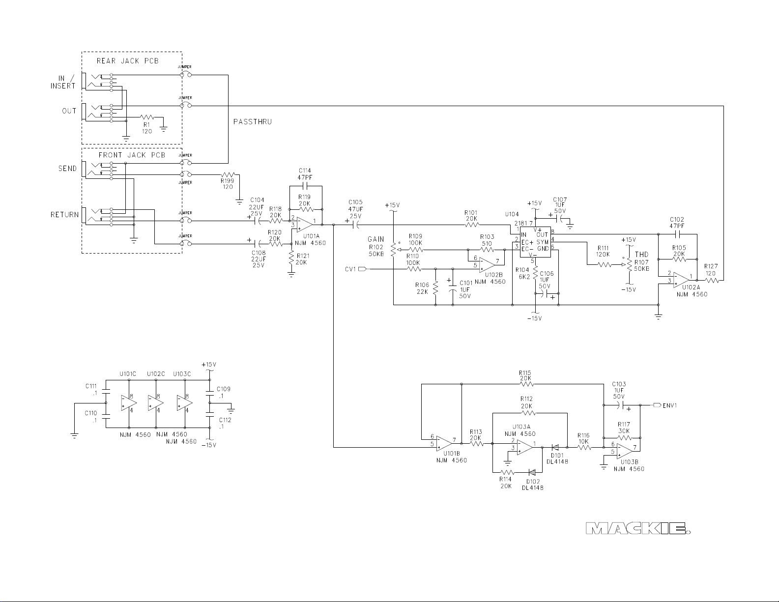
ULTRAMIX VCA CIRCUIT
CHANNEL 1 SHOWN
Page 6
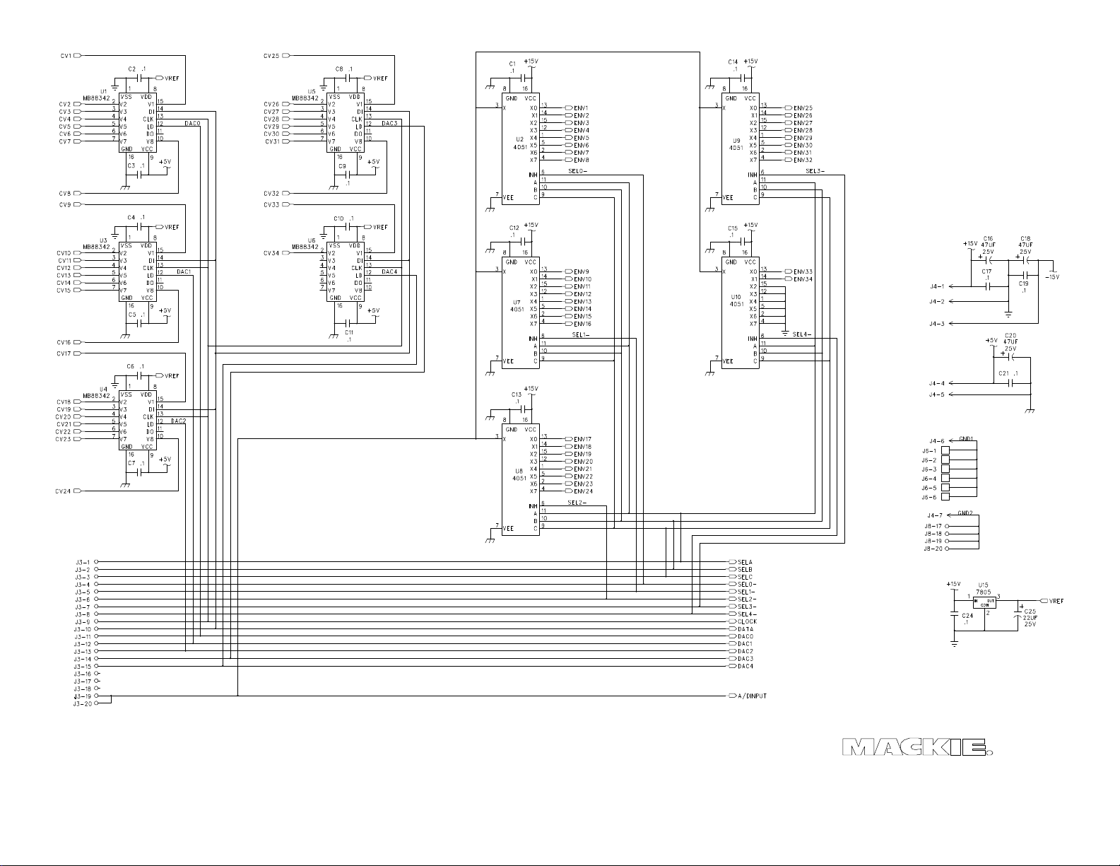
ULTRAMIX VCA BOARD
D/A CIRCUIT
Page 7

LEVEL
THD
LEVEL
THD
ULTRAMIX VCA BOARD
PCB LAYOUT, RIGHT HALF
Page 8

ULTRAMIX VCA BOARD
PCB LAYOUT, LEFT HALF
Page 9

J2 (J38 on front jack PCB) J1
CH 17 RETURN -
1
2
CH 17 RETURN +
CH 1 OUT
1
2
CH 17 OUT
CH 1 RETURN -
3
4
CH 1 RETURN +
CH 1 IN
3
4
CH 17 IN
CH 17 SEND
5
6
CH 1 SEND
CH 2 OUT
5
6
CH 18 OUT
CH 17 SEND GND
7
8
CH 1 SEND GND
CH 2 IN
7
8
CH 18 IN
CH 18 RETURN -
9
10
CH 18 RETURN +
CH 3 OUT
9
10
CH 19 OUT
CH 2 RETURN -
11
12
CH 2 RETURN +
CH 3 IN
11
12
CH 19 IN
CH 18 SEND
13
14
CH 2 SEND
CH 4 OUT
13
14
CH 20 OUT
CH 18 SEND GND
15
16
CH 2 SEND GND
CH 4 IN
15
16
CH 20 IN
CH 19 RETURN -
17
18
CH 19 RETURN +
CH 5 OUT
17
18
CH 21 OUT
CH 3 RETURN -
19
20
CH 3 RETURN +
CH 5 IN
19
20
CH 21 IN
CH 19 SEND
21
22
CH 3 SEND
CH 6 OUT
21
22
CH 22 OUT
CH 19 SEND GND
23
24
CH 3 SEND GND
CH 6 IN
23
24
CH 22 IN
CH 20 RETURN -
25
26
CH 20 RETURN +
CH 7 OUT
25
26
CH 23 OUT
CH 4 RETURN -
27
28
CH 4 RETURN +
CH 7 IN
27
28
CH 23 IN
CH 20 SEND
29
30
CH 4 SEND
CH 8 OUT
29
30
CH 24 OUT
CH 20 SEND GND
31
32
CH 4 SEND GND
CH 8 IN
31
32
CH 24 IN
CH 21 RETURN -
33
34
CH 21 RETURN +
CH 9 OUT
3334CH 25 OUT
GND
1
2
GNDJ5(J125 on front jack PCB)
GND
3
4
GND
CH 22 RETURN -
1
2
CH 22 RETURN +
GND
5
6
GND
CH 6 RETURN -
3
4
CH 6 RETURN +
CH 9 IN
7
8
CH 25 IN
CH 22 SEND
5
6
CH 6 SEND
CH 10 OUT
9
10
CH 26 OUT
CH 22 SEND GND
7
8
CH 6 SEND GND
CH 10 IN
11
12
CH 26 IN
CH 23 RETURN -
9
10
CH 23 RETURN +
CH 11 OUT
13
14
CH 27 OUT
CH 7 RETURN -
11
12
CH 7 RETURN +
CH 11 IN
15
16
CH 27 IN
CH 23 SEND
13
14
CH 7 SEND
CH 12 OUT
17
18
CH 28 OUT
CH 23 SEND GND
15
16
CH 7 SEND GND
CH 12 IN
19
20
CH 28 IN
CH 24 RETURN -
17
18
CH 24 RETURN +
CH 13 OUT
21
22
CH 29 OUT
CH 8 RETURN -
19
20
CH 8 RETURN +
CH 13 IN
23
24
CH 29 IN
CH 24 SEND
21
22
CH 8 SEND
CH 14 OUT
25
26
CH 30 OUT
CH 24 SEND GND
23
24
CH 8 SEND GND
CH 14 IN
27
28
CH 30 IN
CH 25 RETURN -
25
26
CH 25 RETURN +
CH 15 OUT
29
30
CH 31 OUT
CH 9 RETURN -
27
28
CH 9 RETURN +
CH 15 IN
31
32
CH 31 IN
CH 25 SEND
29
30
CH 9 SEND
CH 16 OUT
33
34
CH 32 OUT
CH 25 SEND GND
31
32
CH 9 SEND GND
CH 16 IN
3536CH 32 IN
CH 26 RETURN -
33
34
CH 26 RETURN +
LEFT OUT
3738RIGHT OUT
CH 27 RETURN -
1
2
CH 27 RETURN +
-15 VDC
3
CH 11 RETURN -
3
4
CH 11 RETURN +
+5 VDC
4
CH 27 SEND
5
6
CH 11 SEND
DGND5CH 27 SEND GND
7
8
CH 11 SEND GND
GND6CH 28 RETURN -
9
10
CH 28 RETURN +
GND7CH 12 RETURN -
11
12
CH 12 RETURN +
CH 28 SEND
13
14
CH 12 SEND
J3
CH 28 SEND GND
15
16
CH 12 SEND GND
SEL A
1
2
SEL B
CH 29 RETURN -
17
18
CH 29 RETURN +
SEL C
3
4
SEL 0-
CH 13 RETURN -
19
20
CH 13 RETURN +
SEL 1-
5
6
SEL 2-
CH 29 SEND
21
22
CH 13 SEND
SEL 3-
7
8
SEL 4-
CH 29 SEND GND
23
24
CH 13 SEND GND
CLOCK
9
10
DATA
CH 30 RETURN -
25
26
CH 30 RETURN +
DAC 0
11
12
DAC 1
CH 14 RETURN -
27
28
CH 14 RETURN +
DAC 2
13
14
DAC 3
CH 30 SEND
29
30
CH 14 SEND
DAC 4
15
16
N/C
CH 30 SEND GND
31
32
CH 14 SEND GND
N/C
17
18
N/C
CH 31 RETURN -
33
34
CH 31 RETURN +
A/D INPUT
19
20
A/D INPUT
CH 32 RETURN -
1
2
CH 32 RETURN +
CH 16 RETURN -
3
4
CH 16 RETURN +
CH 32 SEND
5
6
CH 16 SEND
CH 32 SEND GND
7
8
CH 16 SEND GND
RIGHT RETURN -
9
10
RIGHT RETURN +
LEFT RETURN -
11
12
LEFT RETURN +
RIGHT SEND
13
14
LEFT SEND
RIGHT SEND GND
15
16
LEFT SEND GND
CH 5 RETURN - 35 36 CH 5 RETURN +
CH 21 SEND 37 38 CH 5 SEND
CH 21 SEND GND 39 40 CH 5 SEND GND J6
CH 10 RETURN - 35 36 CH 10 RETURN + LEFT IN 39 40 RIGHT IN
CH 26 SEND 37 38 CH 10 SEND
CH 26 SEND GND 39 40 CH 10 SEND GND J4
J7 (J60 on front PCB) GND 2
CH 15 RETURN - 35 36 CH 15 RETURN +
CH 31 SEND 37 38 CH 15 SEND
CH 31 SEND GND 39 40 CH 15 SEND GND
J8 (J82 on front PCB)
+15 VDC 1
GND 17 18 GND
GND 19 20 GND
ULTRAMIX VCA BOARD
JUMPER PINOUT
Page 10

ULTRAMIX LOGIC BOARD SCHEMATIC
Page 11

ULTRAMIX LOGIC PCB LAYOUT
Page 12

ULTRAMIX POWER SUPPLY
SCHEMATIC AND PCB LAYOUT
Page 13

ULTRAPILOT FADER BOARD
SCHEMATIC , SHEET 1 OF 2
Page 14

ULTRAPILOT FADER BOARD
SCHEMATIC , SHEET 2 OF 2
Page 15

ULTRAPILOT FADER BOARD
PCB LAYOUT
Page 16

ULTRAPILOT CONTROL BOARD
SCHEMATIC
Page 17

ULTRAPILOT CONTROL BOARD
PCB LAYOUT
 Loading...