


© Lumina Power, Inc
New Source Technology, LLC
6678 Owens Drive, Suite 105, Pleasanton, CA 94588 USA
Ph (+1) 925(462)-6888 Fx (+1) 925(462)-8388
www.newsourcetechnology.com
sales@newsourcetechnology.com
LDD-3000 CW Laser Diode Driver
02001101 Rev1 Page 1 of 16
USER MANUAL

Table of Contents
Product Overview 3
Explanation of Symbols 4
Theory of Operation 5
LDD-3000 Specifications 7
LDD-3000 Interface 9
Installation and Operation 12
Tables and Figures
Figure 1 LDD-3000 Block Diagram 6
Figure 2 LDD-3000 Chassis Outline Drawing 8
Table 1 LDD-3000 Interface 9
Figure 3 LDD-3000 Interface Schematic 11
Figure 4 LDD-3000 Input/Output Connections 12
Table 2 LDD-3000 AC Input Requirements 14
02001101 Rev1 Page 2 of 16

Product Overview
The LDD-3000 laser diode driver is intended for OEM laser applications using high
power diode lasers. It has been designed to be integrated into systems for
maximum performance at a cost far below traditional laboratory and scientific
laser diode drivers.
The LDD-3000 utilizes a proprietary low loss, high frequency power factor
correction circuit which keeps power factor above 0.98. Power factor corrected
powers supplies use up to 30% less input current and meet stringent IEC
harmonic requirements. The output inverter is state-of-the-art zero voltage
switching (ZVS) inverter which permits very high frequency conversion with
minimum losses.
As a laser diode driver, the LDD-3000 power supply acts as a current source and
delivers constant current based on the input program signal, Iprogram(+), which
is normally 0-10V. An optional RS-232 interface is available. All units are
configured with a maximum current and maximum voltage capability, depending
on the user’s requirements. The LDD-3000 will deliver current, as programmed,
into any load, providing the voltage requirements of that load do not exceed the
maximum rated output voltage of the unit. When the required compliance voltage
is greater than the maximum rated output voltage of the unit, the unit will limit
output current.
02001101 Rev1 Page 3 of 16

Explanation of Symbols
Hazard: This equipment produces high voltages
which can be fatal. Only service personnel of Lumina
Power, Inc. are qualified to service this equipment.
High Voltage Present: This power supply
produces lethal high voltages. Only service personnel
of Lumina Power, Inc. are qualified to service this
equipment. Only qualified service personnel are
permitted to install this power supply.
02001101 Rev1 Page 4 of 16

LDD-3000 Diode Driver Theory of Operation
(Refer to Figure 1)
The LDD-3000 laser diode driver was designed specifically for the OEM high
power CW laser diode systems. OEM power supplies for the laser diode industry
have the following requirements:
Safe laser diode operation
Broad range of control of output current
Safe rise/fall times
Compact size
Power factor correction to conform with CE requirements
Low conducted electromagnetic emissions
Low leakage for medical applications
Referring to the Figure 1, “LDD-3000 Laser Diode Power Supply” block diagram,
the following is a brief description of operation.
AC Input Power Circuitry
AC input power is processed through a line filter to reduce the conducted EMI to
an acceptable level. The LDD-3000 line filter has minimum capacitance to ground
to minimize leakage currents.
Power Factor Correction Boost Inverter
The rectified input power is next applied to power factor boost inverter. This
inverter boosts the input voltage to 400VDC. In the process of boosting the input
AC voltage, the input AC current is adjusted so that is always in phase with the
input AC voltage. Without this power factor correction circuit, the AC input
current would be delivered to the power supply in high amplitude, narrow spikes,
having a high harmonic content. With power factor correction, the non-50/60 Hz
harmonics are reduced to near zero. Since only the fundamental frequency is
now used to deliver power, the efficiency of the power supply is improved
considerably.
One problem with standard input power factor correction circuits is that a high
frequency switching circuit is placed across the line in the input side of the
traditional input capacitor filter. This circuit results in substantial switching noise
conducted to the line. Lumina Power employs a proprietary soft-switching boost
inverter which produces minimum switching noise, reduces switching losses, and
results in a smaller heat sink associated with the power factor circuit.
Zero Voltage Switching (ZVS) Inverter
The ZVS inverter and the output transformer are used to step the 400VDC bus
down to the appropriate output value. The ZVS inverter is the most modern high
frequency/low loss/low noise topology utilized in power electronics today.
Instead of running the inverter in a traditional PWM mode, the inverter is run in a
02001101 Rev1 Page 5 of 16

phase shift mode. With the appropriate output inductor and the appropriate
capacitance across each switching device - in this case MOSFETS - there are
virtually no switching losses in the inverter. The only losses in the devices are I2R
losses associated with the Drain/Source resistance of the MOSFETS. Therefore,
the ZVS inverter also contributes to reduced losses, reduce EMI noise and a
reduction in overall system heatsink requirements.
Output Circuit
The output filter is a two stage RC filter designed to keep ripple and output noise
very low. For lower power units, such as the LDD-3000-250, a single stage filter
is used.
Control Circuit
The control circuit handles all the responsibilities associated with safe operation of
the laser diode. Controlled rise and fall times, as well as tight current regulation,
overvoltage and over power protection are controlled and monitored in the
control circuit.
Auxiliary Power
All internal power supply requirements as well as the external +/-15V and +5V
power supplies are derived from the power factor control boost inductor. All
auxiliary power supplies are regulated by standard linear regulators.
02001101 Rev1 Page 6 of 16
Figure 1
LDD-3000 Block Diagram

LDD-3000-XX-YY SPECIFICATIONS
XX = Iout
Model Pout
YY = Vout
max
Iout
max
XX * YY cannot exceed Pout
max
Input Voltage Size (L x W x H)
max
max
Can be configured
LDD-3000-XX-YY 3000W
Auxiliary Outputs: +5V @0.25A
+15V @0.25A
-15V @0.25A
XX= Maximum rated output current YY=Maximum compliance voltage
RS-232 Option available
Other outputs available upon request
from 50A to 200A
200-240VAC
17” x 16.5” x 3.5”
43.2cm x 42cm x 8.9cm
Input
Voltage: 200-240VAC, 50/60 Hz, 22A@208VAC
Power Factor: >.98
Interface
Connector: 15 Pin “D” Sub Female
Current Program: 0-10V for 0-Max Current
Current Monitor: 0-10V for 0-Max Current
Voltage Monitor: 0-10V for 0-Max Voltage
Performance
Pulse Width Range: 5msec to CW
Rise/Fall Time: ~1msec (10% to 90% Full Current) 600usec available upon request
Current Regulation: 0.5% of Maximum output current
Temperature Drift: 0.5% over temperature range after 30 minute warmup (<0. 5 % in first 30 mi nut es)
Current Ripple: <0.5% of maximum output current
Current Overshoot: <1% of maximum output current
Power Limit: Limited to maximum power with power fold-back circuit
Environment
Operating Temp: 0 to 40 oC
Storage: -20 to 85
Humidity: 0 to 90% non-condensing
Cooling: Forced air
o
C
Regulatory
Leakage Current: <350uA
Approvals:
Industrial Safety: IEC60950-1:2001 (1st Edition), EN 60950-1,2001, UL60950-1, CSA22.2 No.
60950-03
Emissions/Immunity: FCC 47 CFR Class A Emissions, EN55011:1998 Group 1 Class A Emissions,
EN61000-3-2 Limits for harmoni c curre nt emissions, EN 610000303 Flicker,
EN60601-1-2:2001 Electromagnetic emissions and immunity for medical
equipment
02001101 Rev1 Page 7 of 16

02001101 Rev1 Page 8 of 16
Figure 2
LDD-3000 Outline Drawing

LDD-3000-XX-YY Interface
Connector Type: 15 pin D-sub Female
(Refer to Figure 3. LDD-3000 Interface Schematic)
Pin # LDD-3000 Pin
1
2 Current Limit
3
4 GND
5
6
7
8
9 GND
10,11
12
13,14
15 GND Interface return
Name
Enable
(input)
Interlock
(input)
Vout Monitor:
(output)
Iout Monitor
(output)
Iprogram(+):
(input)
Pulse Control
(input)
+5V @ 0.25A
(output)
-15V @0.25A
(output)
+15V @0.25A
(output)
1. Pin 5: If maximum compliance voltage is less than 10V, Vout Monitor will read output voltage
directly. If maximum compliance voltage is greater than 10V, then Vout Monitor will be scaled
such that 0-10V = 0-Voutmax. Applying a program voltage greater than 10.5 volts will latch
power supply. Output current will not exceed 105% of rating.
Functional Voltage Level Description
High=RUN=+5V to +15V
Low = OFF = 0V
0-10V = 1- 100% Output
Current
Open = OFF
Connect to GND = RUN
0 – 10V = 0 – Vout
0 – 10V = 0 – Iout
0 – 10V = 0 – Iout
TTL High = On
TTL Low = OFF
Default = On
Auxiliary +5V power supply for user. Up to 0.25A output current
Auxiliary -15V power supply for user. Up to –0.25A output current
Auxiliary +15V power supply for user. Up to 0.25A output current
max
max
max
The Enable function turns the output section of the power supply ON
and OFF. When the power supply is enabled, current is delivered to
load as programmed via Iprogram(+), Pin 7, if the Pulse Control,
Pin 8, is High and the Interlock, pin 3 is connected to interface GND.
Rise times resulting from Enable are approximately 25msec. For
pulsing, the Enable function should be set to ON, and the Pulsing
Control, Pin 8, should be used.
This is secondary protection. Output current will be limited by this
signal. Leaving it open defaults at 105% current.
The Interlock function must be connected to GND in order for outp ut
current to be delivered. It can be used for external interlock functions
such as door or overtemp switches.
The output voltage of the supply can be monitored by Vout Monitor.
For LDD-3000’s with a maximum rated output voltage less than 10V,
Vout Monitor = Vout. For output voltages greater than or eq ual to
10V, 0-10V = 0 - Vout
The output current of the supply can be monitored by Iout Monitor.
The power supply output current is set by applying a 0-10V analog
signal to Iprogram(+).
The output may be pulsed by applying a TTL signal to Pulse Control,
pin 8. The amplitude of the output current pulse is determined by the
voltage programmed via Pin 7, Iprogram(+). Rise/fall times of
<1msec are typical. Rise fall times of 500usec can be achieved with
special order.
capability.
available.
available.
max
.
Table 1: LDD-3000 Interface
02001101 Rev1 Page 9 of 16

Optional RS-232 Protocol
LDD-3000-XX-YY-RS
Refer to Figure 4, LDD-3000 Outline Drawing for location of RS-232 Connector.
The RS232 interface for Lumina supplies has the following characteristics:
Baud rate: 9600
Command format: ASCII characters terminated by carriage return
Reply formats: ASCII characters terminated by carriage return
Connection: 9 Pin “D” Female (Tx: Pin 2, Rx: Pin 3, GND: Pin 5)
The interface supports programming the output current and power limit of the supply and
reading back the output current and voltage. The output can be turned on and off with a
command as well.
Command Reply Function
Pxx.xx@xx.xx<cr> <cr> Program output current to max rated output current
xx.xx between 0 and 10.00 = 0 – Iout
(Note: Pxx.xx<cr> will also work)
I<cr> xx.xx<cr> Read output current xx.xx between 0 and 10.00 = 0
Iout
V<cr> xx.xx<cr> Read output voltage xx. xx between 0 and 10.00 = 0
to Vout
ON<cr> <cr> Enable supply output
OFF<cr> <cr> Disable supply output
Jhkhkh<cr> ?<cr> Response to unrecognized command
Numbers sent to the supply should be in fixed point decimal format. The numbers sent
back will have four digits and a decimal point, but the resolution is limited to 12 bits and
the accuracy is limited by the specifications of the supply.
max
max
max
Connections to Analog Interface when using RS-232
Interlock function, Pin 3, must be employed whether using LDD analog interface or RS-
232. None of the other controls in the Analog interface need be utilized when using the
RS-232 optional interface.
02001101 Rev1 Page 10 of 16
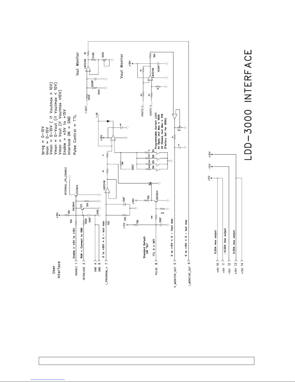
LDD-3000-XX-YY Interface Schematic
02001101 Rev1 Page 11 of 16
Figure 3

Installation and Operation of
LDD-3000 Diode Drivers
There are two 8-32 PEM nuts on each side of the LDD-3000 for mounting the unit in a
system. Refer to Figure 2, the LDD-3000 Outline Drawing, for the location of these PEM
nuts Also, there are four 10-32 PEM nuts on the bottom of the chassis for mounting
purposes. If used, mounting screws should not penetrate more than 3/8” into the chassis.
LDD-3000 diode drivers are air cooled by internal fans. Do not restrict air
flow near the input or output air vents of the power supply. If the unit
overheats due to restricted air flow, it will shut down and remain off until the
unit has cooled to a safe operating temperature.
Because LDD-3000 units are designed for OEM applications, the user must
connect AC input power to the power supply chassis. Any input AC voltage
must be considered extremely dangerous, and as such, care must be taken to
connect AC input power to the unit.
IMPORTANT INSTALLATION NOTE
SAFETY WARNING
1. Connecting to Laser Diode: Figure 4 shows the location of the LDD-3000
output terminals. Connect diode laser load to the output terminals. Although CW
diode laser applications are generally free of voltage spikes associated with high
speed Quasi-CW applications, it is still good practice to keep connections between
the diode laser and power supply as short as possible to avoid I2R losses in the
wire.
2. Interface Connection: Connect user system to 15 pin D-sub connector shown in
Figure 4. (Although the user interface is typically designed by the user, Lumina
02001101 Rev1 Page 12 of 16
Figure 4
LDD-3000 Input/Output Connections

Power can provide any assistance necessary to modify interface program and
monitor levels) See Table 1 and Figure 3 for description of LDD-3000 Interface
and the associated simplified interface schematic.
Make sure when connecting interface that the current program
setting, Iprogram(+), is set no higher then the value required for
operation. When AC power is applied and system is Enabled,
output current will rise to this program value
IMPORTANT NOTE
3. Interface Information before applying AC Power: The unit may be
programmed for output current via Pin-7, the Iprogram function. But there are
three interface control signals which must be properly set before the output will
deliver current as programmed by Iprogram.
a. INTERLOCK: Pin 3, the Interlock, must be grounded via Pins 4, 9 or 15
in order for the output to deliver current.
b. PULSE CONTROL: Pin 8, the PULSE CONTROL pin, must be a TTL
HIGH in order for the output to deliver current. The PULSE CONTROL
function is used when the user wants to pulse the output. Because the
default for PULSE CONTROL is TTL HIGH + ON, for CW operation,
the PULSE CONTROL pin may be left open. Refer to Section 7 for more
information on pulsing.
c. ENABLE: Pin 1, the ENABLE signal is a 5V to 24V signal used to turn
the output section on. The ENABLE circuitry incorporates a soft start
function which ensures rise times of approximately 15 to 20msec.
CH 1
Iout
20A/div
CH 2
ENABLE
Typical Response of Iout to ENABLE signal
d. Iprogram: Pin 7. A 0-10V signal results in 0 to Iout
, as long as the
max
rated compliance voltage of the driver is not exceeded.
02001101 Rev1 Page 13 of 16
4. Operating the LDD:
a. AC Input Power Connection: Input power is shown in Table 2. Connect
AC power and Earth Ground connections to power supply input power
terminals. Refer to Figure 4 for location of AC Input.
MODEL INPUT POWER
LDD-3000-XX-YY 200-240 VAC, 50/60 Hz, 21A @200VAC
Table 2: LDD-3000 AC Input Power Requirements
IMPORTANT APPLICATON NOTE REGARDING AC INPUT POWER
AC Input wires and Earth Ground wire should be at least #12 AWG, rated for at
least 300V and 105DegC.
IMPORTANT SYSTEM NOTE ON AC INPUT POWER
LDD-3000 units are fused on both input lines. It does not matter which of the
two AC inputs are designated Line or Neutral.
b. INTERFACE SETTINGS: Make sure Interlock, Pin 3, is connected to
GND and Pulse Control, Pin 8, is set to TTL HIGH.
c. APPLY INPUT AC POWER Turn ON AC power. After a few seconds
the power supply fans will begin to run.
d. PROGRAMMING OUTPUT CURRENT Program LDD-3000 power
supply for desired output current. A 0-10V signal applied to Iprogram,
Pin 7, will program the LDD-3000 diode driver for 0 to maximum rated
output current.
When the power supply is enabled using the ENABLE signal, internal soft
start functions limit the rise time of the output current to approximately
20msec. Once the power supply is enabled, the rise/fall time of the output as a
result of programming via the Iprogram(+) signal is approximately 600usec.
IMPORTANT APPLICATION NOTE
e. ENABLE OUTPUT Apply +5V to +15V to Enable, Pin 1. The LDD-
3000 will deliver output current as programmed.
5. Monitoring LDD output and performance:
a. Current Monitor Power supply output current can be monitored via pin
6, Iout Monitor. A 0-10V signal will represent the output current from 0
to maximum rated output current.
02001101 Rev1 Page 14 of 16
b. Voltage Monitor Power supply output voltage can be monitored via pin
5, Vout Monitor. A 0-10V signal will represent the output voltage from 0maximum rated output voltage.
6. Pulsed Operation:
The LDD-3000 is intended for CW applications. However due the fast response
achievable with very high frequency switchmode power supplies, it is possible to
pulse diode lasers at sub QCW speeds. The typical rise and fall times of the LDD3000 units are approximately 600 usec. Therefore a rep rate of 200Hz to 400Hz is
possible. Pulsing can be accomplished via the PULSE CONTROL function on Pin
8. A TTL HIGH must be applied to pulse the output on. The user may configure
the pulse train as desired. Typical performance is shown below.
CH 1
Iout
20A/div
Typical LDD-3000 Rise Fall Time
CH 2
ENABLE
Consult the factory for faster rise/fall times.
NOTE: It is not possible to use Enable, Pin 1, for pulsing since the ENABLE circuit
includes a “soft start” is intended for turning on the power supply output slowly. The
Enable function controls several soft-start features which do not permit pulsing.
NOTE: For faster pulsing, refer to the data sheet for Lumina Power’s LDQCW power
supplies. These units have rise/fall times of less than 25usec and can achieve output
currents up to 200A. These units can pulse at frequencies up to 5khz, depending on the
average power required.
7. Servicing the LDD-3000:
LDD-3000 units have no serviceable parts. Do not attempt to repair or service this
unit in the field. Removing tamper seals from chassis will void warranty. For
further information, contact Lumina Power at 978-241-8260.
02001101 Rev1 Page 15 of 16

Rev ECO Description Date
Doc
Control
1 7062 Release 3/9/12 MJ
© Lumina Power, Inc
02001101 Rev1 Page 16 of 16
Contact US:
New Source Technology, LLC
6678 Owens Drive, Suite 105, Pleasanton, CA 94588 USA
Ph (+1) 925(462)-6888 Fx (+1) 925(462)-8388
www.newsourcetechnology.com
sales@newsourcetechnology.com
 Loading...