

Page 1
SERVICE MANUAL
Sec. 1: Main Section
I
Specifications
I
Preparation for Servicing
I
Adjustment Procedures
I
Schematic Diagrams
I
CBA’s
Sec. 2: Deck Mechanism Section
I
Standard Maintenance
I
Alignment for Mechanism
I
Disassembly/Assembly of Mechanism
I
Alignment Procedures of Mechanism
Sec. 3: Exploded views
and Parts List Section
I
Exploded views
I
Parts List
VIDEO CASSETTE RECORDER
VCR425
PAL
Page 2

MAIN SECTION
VIDEO CASSETTE RECORDER
VCR425
Sec. 1: Main Section
I
Specifications
I
Preparation for Servicing
I
Adjustment Procedures
I
Schematic Diagrams
I
CBA’s
TABLE OF CONTENTS
Specifications. . . . . . . . . . . . . . . . . . . . . . . . . . . . . . . . . . . . . . . . . . . . . . . . . . . . . . . . . . . . . . . . . . . . . . . . . . 1-1-1
Important Safety Precautions. . . . . . . . . . . . . . . . . . . . . . . . . . . . . . . . . . . . . . . . . . . . . . . . . . . . . . . . . . . . . . 1-2-1
Standard Notes for Servicing. . . . . . . . . . . . . . . . . . . . . . . . . . . . . . . . . . . . . . . . . . . . . . . . . . . . . . . . . . . . . .1-3-1
Preparation for Servicing . . . . . . . . . . . . . . . . . . . . . . . . . . . . . . . . . . . . . . . . . . . . . . . . . . . . . . . . . . . . . . . . .1-4-1
Cabinet Disassembly Instructions . . . . . . . . . . . . . . . . . . . . . . . . . . . . . . . . . . . . . . . . . . . . . . . . . . . . . . . . . . 1-5-1
Electrical Adjustment Instructions . . . . . . . . . . . . . . . . . . . . . . . . . . . . . . . . . . . . . . . . . . . . . . . . . . . . . . . . . . 1-6-1
Block Diagrams . . . . . . . . . . . . . . . . . . . . . . . . . . . . . . . . . . . . . . . . . . . . . . . . . . . . . . . . . . . . . . . . . . . . . . . . 1-7-1
Function Indicator Symbols . . . . . . . . . . . . . . . . . . . . . . . . . . . . . . . . . . . . . . . . . . . . . . . . . . . . . . . . . . . . . . . 1-7-9
Schematic Diagrams / CBA’s and Test Points. . . . . . . . . . . . . . . . . . . . . . . . . . . . . . . . . . . . . . . . . . . . . . . . . 1-8-1
Waveforms. . . . . . . . . . . . . . . . . . . . . . . . . . . . . . . . . . . . . . . . . . . . . . . . . . . . . . . . . . . . . . . . . . . . . . . . . . . . 1-9-1
Wiring Diagrams . . . . . . . . . . . . . . . . . . . . . . . . . . . . . . . . . . . . . . . . . . . . . . . . . . . . . . . . . . . . . . . . . . . . . . 1-10-1
IC Pin Function Descriptions . . . . . . . . . . . . . . . . . . . . . . . . . . . . . . . . . . . . . . . . . . . . . . . . . . . . . . . . . . . . . 1-11-1
Lead Identifications . . . . . . . . . . . . . . . . . . . . . . . . . . . . . . . . . . . . . . . . . . . . . . . . . . . . . . . . . . . . . . . . . . . .1-12-1
Page 3
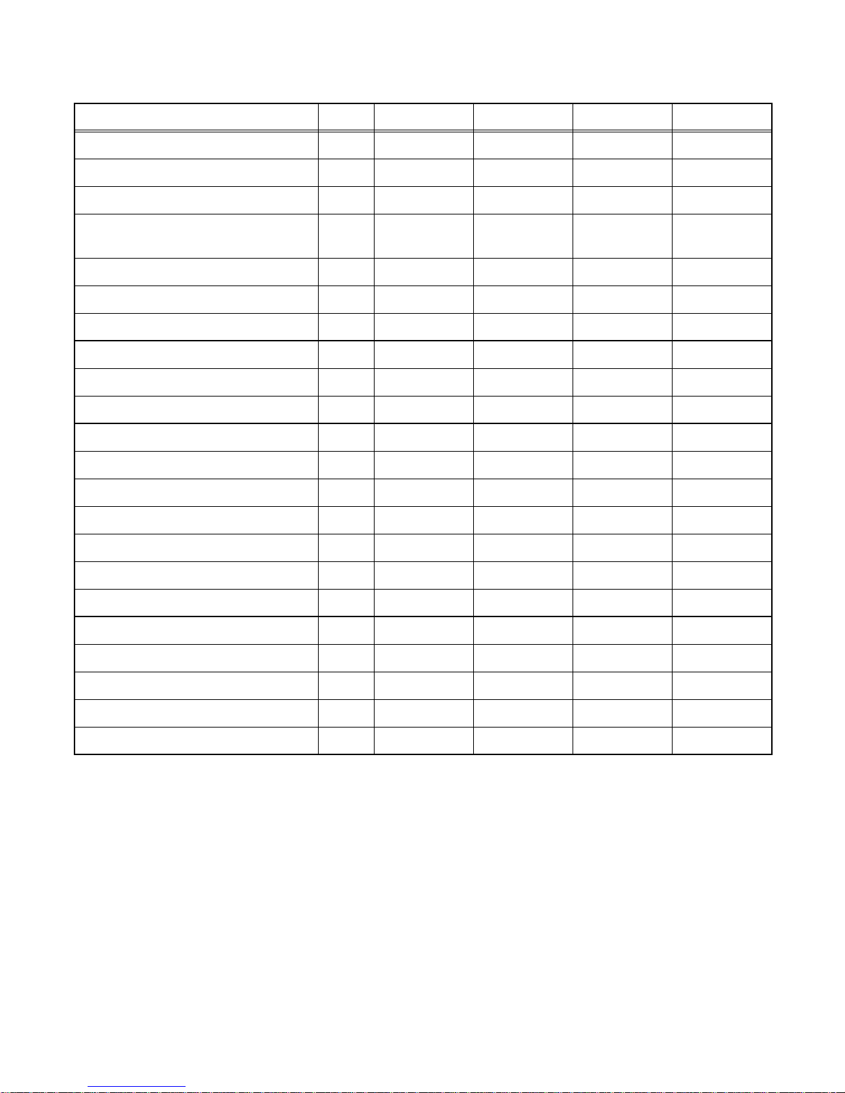
SPECIFICATIONS
Description Unit Minimum Nominal Maximum Remark
1. Video
1-1. Video Output (PB) Vp-p 0.8 1.0 1.2 FL6A
1-2. Video Output (R/P) Vp-p 0.8 1.0 1.2
1-3. Video S/N Y (R/P) dB 40 45
1-4. Video Color S/N AM (R/P) dB 37 41 SP Mode
1-5. Video Color S/N PM (R/P) dB 30 36 SP Mode
1-6. Resolution (PB) Line 230 245 SP Mode
2. Servo
2-1. Jitter Low µsec 0.07 0.12 SP Mode
2-2. Wow & Flutter % 0.3 0.5 SP Mode
3. Normal Audio
3-1. Output (PB) dBV -9 -6 -3 SP Mode
3-2. Output (R/P) dBV -9 -6 -1.5 SP Mode
3-3. S/N (R/P) dB 36 41 SP Mode
3-4. Distortion (R/P) % 1.0 4.0 SP Mode
3-5. Freq. resp (R/P) at 200Hz dB -7 -4 SP Mode
(-20dB ref. 1kHz) at 6kHz dB -10 -4 SP Mode
SP Mode,
W/O Burst
4. Tuner
4-1. Video output Vp-p 0.8 1.0 1.2 E-E Mode
4-2. Video S/N dB 39 42 E-E Mode
4-3. Audio output dB -10 -6 -2 E-E Mode
4-4. Audio S/N dB 40 46 E-E Mode
: Nominal specs represent the design specs. All units should be able to approximate these – some will exceed
Note
and some may drop s lightly bel ow these spec s. Limit sp ecs rep resent the a bsolute wo rst con dition that still migh t
be considered acceptable; In no case should a unit fail to meet limit specs.
1-1-1 HC341SP
Page 4

IMPORTANT SAFETY PRECAUTIONS
Product Safety Notice
Some electrical and mechanical parts have special
safety-related char acteristics which are often not evi dent from visual inspection, nor can the protection
they give necessarily be obtained by replacing them
with components rated for higher voltage, wattage,
etc. Parts that have sp ecial safety characteristi cs are
identified by a ! on schematics and in parts lists. Use
of a substitute replacement that does not have the
same safety characteristics as the recommended
replacement part might create shock, fire, and/or other
hazards. The Prod uct’s Safety is under review continuously and new instructions are issued whenever
appropriate. Prior to shipment from the factory, our
products are carefully inspected to confirm with the
recognized product s afety and electrical codes of the
countries in which they are to be sold. However, in
order to maintain su ch com plian ce, it is equal ly imp ortant to implement the following precautions when a set
is being serviced
Precautions during Servicing
Parts identified by the ! symbol are critical for
A.
safety. Replace only with part number specified.
In addition to safety, other parts and assemblies
B.
are specified for conformance with regulations
applying to spur ious rad iation. T hese m ust also be
replaced only with specified re pla ce men ts .
Examples: RF converters, RF c ables, noise blocking capacitors, and noise blocking f ilters, etc.
Use specified internal wiring. Note especially:
C.
1)Wires covered with PVC tubing
2)Double insulated wires
3)High voltage leads
Use specified insulating materials for hazardous
D.
live parts. Note especially:
1)Insulation tape
2)PVC tubing
3)Spacers
4)Insulators for transistors
When replacing AC primary side components
E.
(transformers, power cord, etc.), wrap ends of
wires securely about the terminals before soldering.
Observe that the wires do not contact hea t produc-
F.
ing parts (heatsinks, oxid e met al film res istors, fusible resistors, etc.).
Check that replaced wires do not contact sharp
G.
edges or pointed parts.
When a power cord h as been repl aced, ch eck that
H.
5 - 6 kg of force in any direction will not loosen it.
.
Also check areas surrounding repaired locations.
I.
Be careful that foreign objects (screws, solder
J.
droplets, etc.) do not remain inside the set.
Crimp type wire connector
K.
The power tr ansformer uses crimp type connectors
which connect the power cord and the primary side
of the transformer. When replacing the transformer,
follow these steps carefully and precisely to prevent shock hazards.
Replacement procedure
1)Remove the old connector by cutting the wires at a
point close to the connector.
Important:
2)Strip about 15 mm of t he insulation fr om the ends
of the wires. If the wires are stranded, twist the
strands to avoid frayed conductors.
3)Align the lengths of the wires to be connected.
Insert the wires fully into the connector.
4)Use a crimping tool to crimp the metal sleeve at its
center. Be sure to crimp ful ly to the complete closure of the tool.
When connecting or disconnecting the internal con-
L.
nectors, first, disco nnect the AC plug from th e AC
outlet.
Do not re-use a connector. (Discard it.)
1-2-1 H8740SFP
Page 5
Safety Check after Servicing
Examine the area surrounding the repaired location for
damage or deterioration. Obse rve that screws, parts,
and wires have been returned to their original positions. Afterwards, do the following tests and confirm
the specified values to verify compliance with safety
standards.
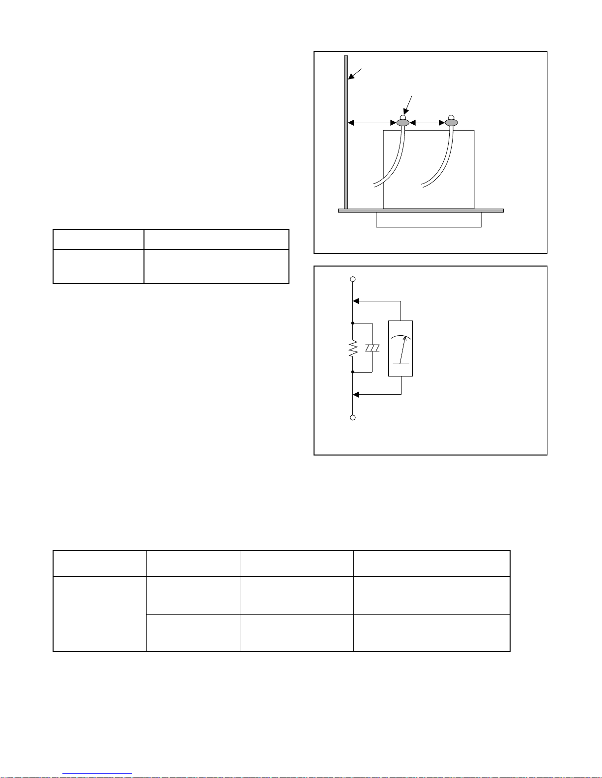
1. Clearance Distance
When replacing primary circuit components, confirm
specified clearan ce distance (d) and (d’ ) between soldered terminals, and between terminals and surrounding metallic parts. (See Fig. 1)
Table 1 : Ratings for selected area
AC Line Voltage Clearance Distance (d) (d’)
230 V
This table is unofficial and for reference only.
Note:
Be sure to confirm the precise values.
≥ 3mm(d)
≥ 6 mm(d’)
2. Leakage Current Test
Confirm the specified (or lower) leakage current
between B (earth ground, power cord plug prongs)
and externally exposed accessible parts (RF terminals, antenna terminals, video and audio input and
output terminals, microphone jacks, earphone jacks,
etc.) is lower than or equal to the specified value in the
table below.
Measuring Method (Power ON) :
Insert load Z between B (earth ground, power cord
plug prongs) and exposed accessible parts. Use an
AC voltmeter to measure acr oss the ter minals of l oad
Z. See Fig. 2 and the following table.
Chassis or Secondary Conductor
Primary Circuit Terminals
dd'
Exposed Accessible Part
Z
One side of
B
Power Cord Plug Prongs
AC Voltmeter
(High Impedance)
Fig. 1
Fig. 2
Table 2: Leakage current ratings for selected areas
AC Line Voltage Load Z Leakage Current (i)
2kΩ RES.
Connected in
230 V
This table is unofficial and for reference only. Be sure to confirm the precise values.
Note:
parallel
50kΩ RES.
Connected in
parallel
i≤0.7mA AC Peak
i≤2mA DC
i≤0.7mA AC Peak
i≤2mA DC
1-2-2 H8740SFP
One side of power cord plug
prongs (B) to:
RF or
Antenna terminals
A/V Input, Output
Page 6
STANDARD NOTES FOR SERVICING
Circuit Board Indications
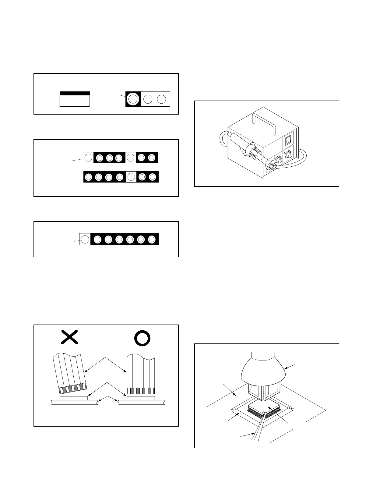
a. The output pin of the 3 pin Regulator ICs is indi-
cated as shown.
Top View
Out
b. For other ICs, pin 1 and every fifth pin are indicated
as shown.
Input
In
Pin 1
c. The 1st pin of every male connector is indica ted as
shown.
Pin 1
Bottom View
5
10
How to Remove / Install Flat Pack-IC
1. Removal
With Hot-Air Flat Pack-IC Desoldering Machine:
(1) Prepare the hot-air flat pack-IC desoldering
machine, then apply hot air to the Flat Pack-IC
(about 5 to 6 seconds). (Fig. S-1-1)
Fig. S-1-1
(2) Remove the flat pack-IC with tweezers while apply-
ing the hot air.
(3) B ottom of the flat pack-IC is fixed with glue to the
CBA; when removing en tire flat pack-IC, fir st apply
soldering iron to c en ter of the flat pack-IC and hea t
up. Then remove (glue will be melted). (Fig. S-1-6)
(4) R elease the fla t pack-IC from the CBA using twee-
zers. (Fig. S-1-6)
.
Instructions for Connectors
1. When you connec t o r di s connec t the FF C ( Flex ible
Foil Connector) cable, be sure to first disconnect
the AC cord.
2. FFC (Flexible Foil Connector) cable should be
inserted parallel into the connector, not at an angle.
FFC Cable
Connector
CBA
* Be careful to avoid a short circuit.
Caution:
1. Do not supply hot air to the chip parts aroun d the
flat pack-IC for over 6 seconds because damage
to the chip parts may occur. Put masking tape
around the flat pack -IC to protect other parts from
damage. (Fig. S-1-2)
2. The flat pack-IC on the CB A is affixed with glue, so
be careful not to break or damage the foil of each
pin or the solder lands under the IC when removing
it.
Hot-air
Flat Pack-IC
Desoldering
CBA
Masking
Tape
Tweezers
Machine
Flat Pack-IC
Fig. S-1-2
1-3-1 NOTE_1
Page 7
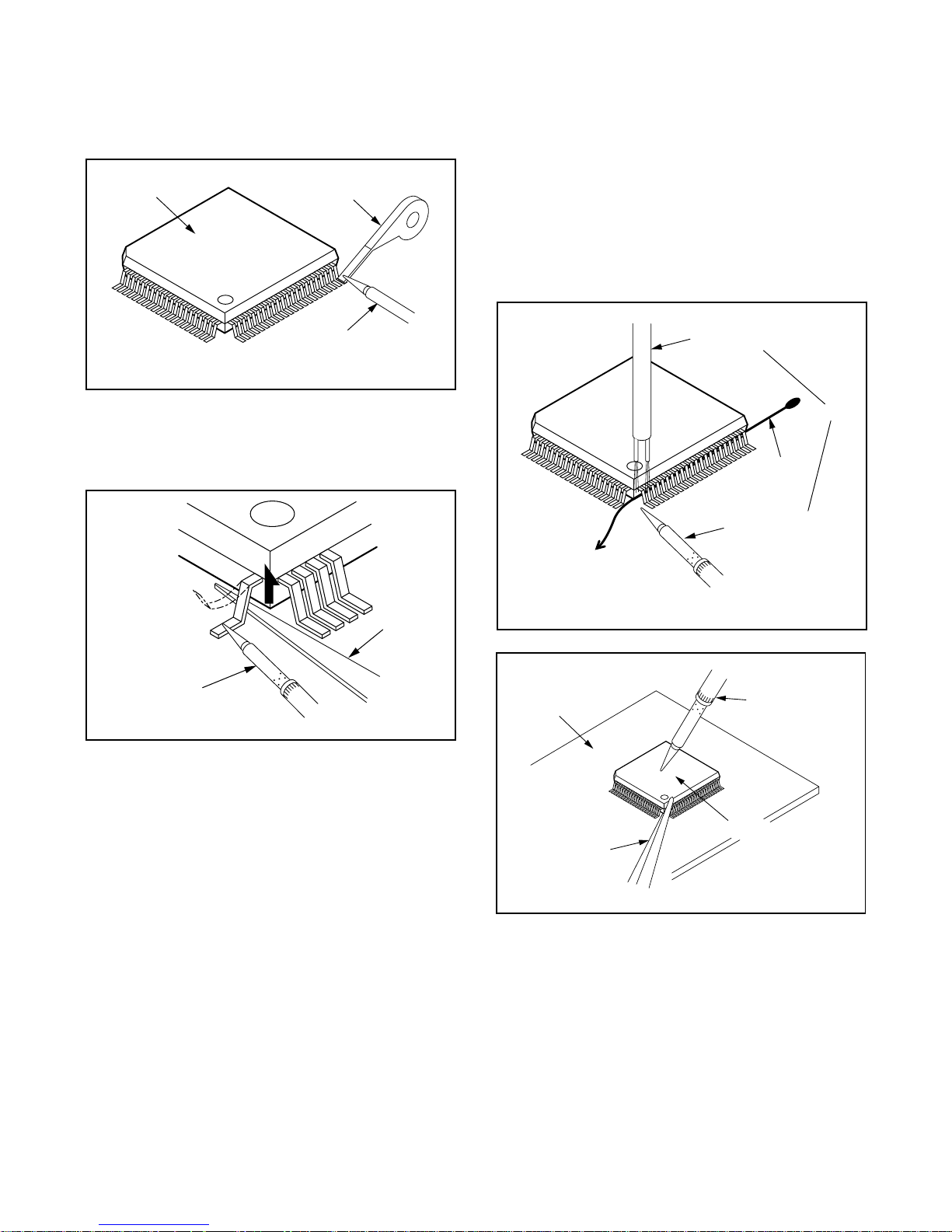
With Soldering Iron:
(1)Using desoldering braid, remove the solder from all
pins of the flat pack-IC. W hen you use solder flux
which is applied t o all pins of the f lat pack-IC, you
can remove it easily. (Fig. S-1-3)
Flat Pack-IC
Desoldering Braid
(4) B ottom of the flat pack-IC is fixed with glue to the
CBA; when removing en tire flat pack-IC, fir st apply
soldering iron to c en ter of the flat pack-IC and hea t
up. Then remove (glue will be melted). (Fig. S-1-6)
(5) R elease the fla t pack-IC from the CBA using twee-
zers. (Fig. S-1-6)
Note:
When using a solde ring iron, care must be taken
to ensure that the flat pack-IC is not being held by
glue. When the flat pack-IC is removed from the
CBA, handle it ge ntl y bec au se it may be damaged
if force is applied.
Soldering Iron
Fig. S-1-3
(2) Lift each lead of the flat pack-IC upward one by
one, using a sharp pin or wire to which sold er will
not adhere (iron wir e). When heating the pi ns, us e
a fine tip soldering iron or a hot air desoldering
machine. (Fig. S-1-4)
Sharp
Pin
Fine Tip
Soldering Iron
Fig. S-1-4
(3)Botto m of the flat pack-IC is fixed with glue to the
CBA; when removing en tire flat pack -IC, first appl y
soldering iron to c ent er of the fla t pa ck - IC an d h eat
up. Then remove (glue will be melted). (Fig. S-1-6)
(4)Relea se th e flat pac k-IC from the CB A us ing twee -
zers. (Fig. S-1-6)
With Iron Wire:
(1)Using desoldering braid, remove the solder from all
pins of the flat pack-IC. W hen you use solder flux
which is applied t o all pins of the f lat pack-IC, you
can remove it easily. (Fig. S-1-3)
(2) Affix the wire to a workbench or solid mounting
point, as shown in Fig. S-1-5.
(3) While heating the pins using a fine tip soldering
iron or hot air blower, pull up t he wir e as t he so lde r
melts so as to lift the IC leads from the CBA contact
pads as shown in Fig. S-1-5
To Solid
Mounting Point
CBA
Tweezers
Hot Air Blower
or
Iron Wire
Soldering Iron
Fig. S-1-5
Fine Tip
Soldering Iron
Flat Pack-IC
Fig. S-1-6
1-3-2 NOTE_1
Page 8
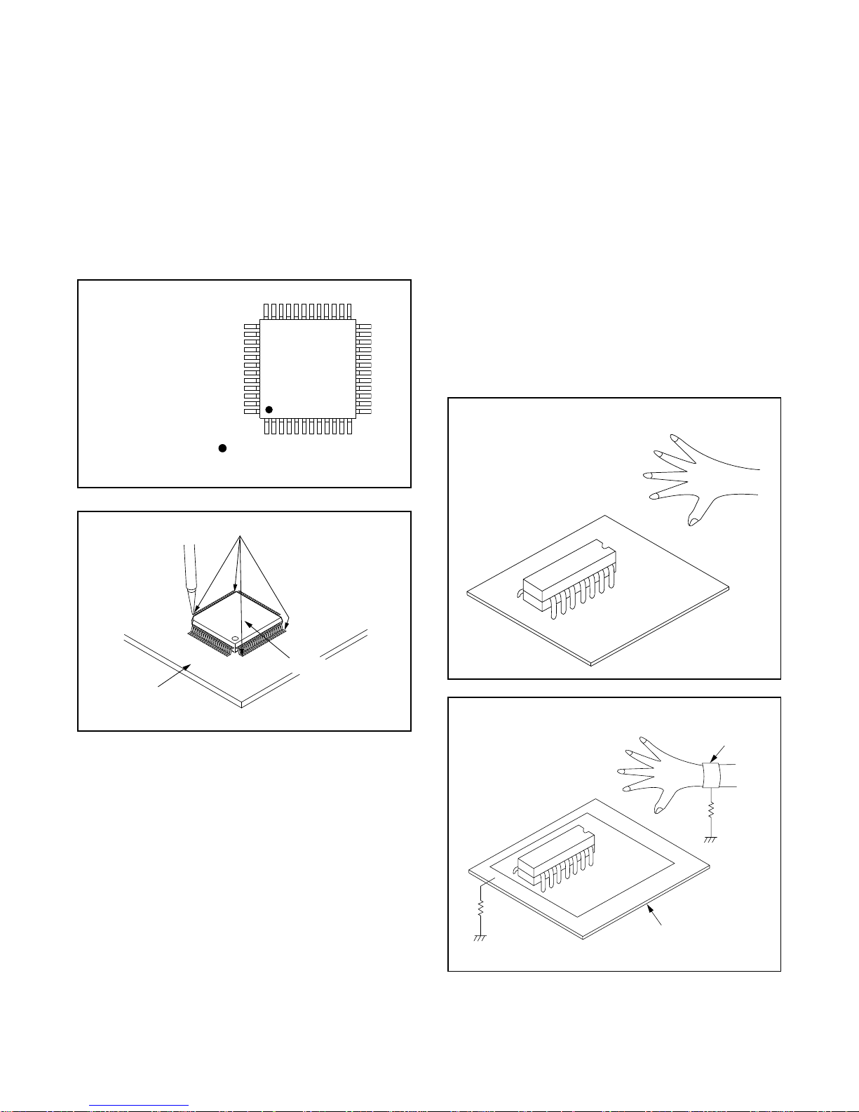
2. Installation
(1) Using desoldering braid, remove the solder from
the foil of each pi n of the flat pack-IC on the CBA
so you can install a replacemen t flat pack-IC more
easily.
(2)The “ I ” mark on the flat pack -IC indicates pin 1.
(See Fig. S-1-7.) Be sure this mar k matches the 1
on the PCB when positioni ng for installation. Then
presolder the four corn ers o f the fl at pac k -IC. (S ee
Fig. S-1-8.)
(3)Solder all pins of the flat pack-IC. Be sure that none
of the pins have solder bridges.
Example :
Pin 1 of the Flat Pack-IC
is indicated by a " " mark.
Fig. S-1-7
Instructions for Handling
Semi-conductors
Electrostatic breakdown of the semi-conductors may
occur due to a poten tial difference c aused by electrostatic charge during unpacking or repair work.
1. Ground for Human Body
Be sure to wear a gr oundin g band (1MΩ) that is properly grounded to re m ov e an y sta tic el ec tric it y that may
be charged on the body.
2. Ground for Workbench
Be sure to place a c onductive sheet or copper plate
with proper grounding (1MΩ) on the workbench or
other surface, where the semi-conductors are to be
placed. Because t he static electric ity charge on c lothing will not escape through the body grounding band ,
be careful to avoid contacting semi-conductors with
your clothing.
< Incorrect >
CBA
Presolder
Flat Pack-IC
Fig. S-1-8
CBA
< Correct >
Grounding Band
1MΩ
CBA
1MΩ
Conductive Sheet or
Copper Plate
1-3-3 NOTE_1
Page 9
PREPARATION FOR SERVICING
How to Enter the Service Mode
About Optical Sensors
Caution:
An optical sensor system is used for the Tape Start
and End Sensors on this equipment. Carefully read
and follow the instruct ions below. Otherwise the unit
may operate erratically.
What to do for preparation
Insert a tape into th e Deck Mechanis m Assembly and
press the PLAY button. The tape will be loaded into
the Deck Mechanism Assembly. Make sure the power
is on, TP507 (SENSOR INHIBITION) to GND. This will
stop the function of Tape Start Sensor, Tape End Sensor and Reel Sensors. (If these TPs are connected
before plugging in the unit, th e functi on of th e sens ors
will stay valid.) See Fig. 1.
Because the Tape End Sensors are inactive, do
Note:
not run a tape a ll th e way t o the s tart or t he en d of the
tape to avoid tape damage.
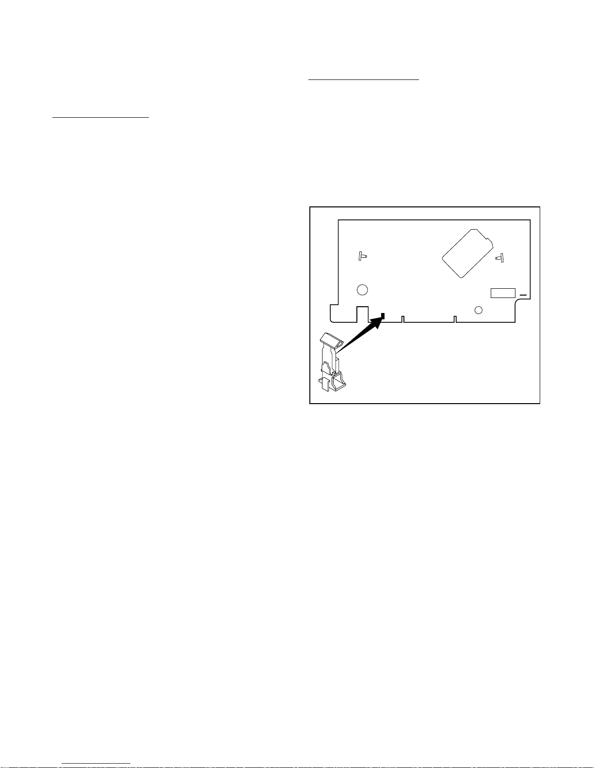
About REC-Safety Switch
Caution:
The REC-Safety Switch is directly mounted on the
Main CBA. When the Dec k Mechanism Assembly is
removed from t he Main CBA for servic ing, this sw itch
does not work automatically.
What to do for preparation
In order to record, pr ess the Rec butt on whil e push ing
REC-SAFETY SW on the Main CBA. See Fig. 1.
Q503
SW506
Q504
TP507
S-INH
(REC-SAFETY SW)
Fig. 1
1-4-1 HC2C0PFS
Page 10
CABINET DISASSEMBLY INSTRUCTIONS
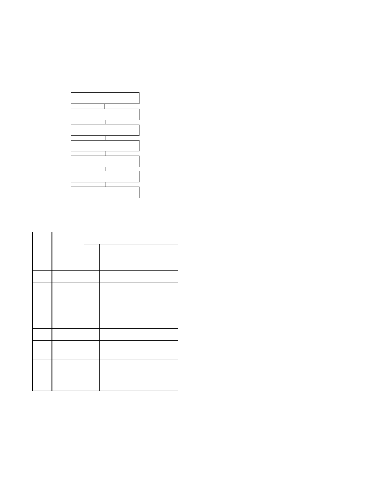
1. Disassembly Flowchart
This flowchart indicate s the disas sembly step s to gain
access to item(s) to be serviced. When reassembling,
follow the steps in reverse order. Bend, route, and
dress the cables as they were originally.
[1] Top Case
[2] Front Assembly
[3] VCR Chassis Unit
[4] Jack CBA
[5] Function CBA
[6] Deck Assembly
[7] Main CBA
2. Disassembly Method
REMOVAL
ID/
LOC.
No.
PART
REMOVE/*UNHOOK/
Fig.
UNLOCK/RELEASE/
No.
UNPLUG/DESOLDER
Note
(1): Identification (location) No. of parts in the figures
(2):Name of the part
(3):Figure Number for reference
(4): Identification of parts to be removed, unhooked,
unlocked, released, unplugged, unclamped, or
desoldered.
P=Spring, L= Locking Tab, S=Screw,
CN=Connector
*=Unhook, Unlock, Release, Unplug, or Desolder
e.g. 2(S-2) = two Screws (S-2),
2(L-2) = two Locking Tabs (L-2)
(5):Refer to “Reference Notes.”
Reference Notes
CAUTION: Locking Tabs (L-1) and (L-2) are fragile.
Be careful not to break them.
1. Release Locking Tab (L-3) and remove Screw
(S-2), five Screws (S-3), three Screws (S-4) and
Screw (S-5). Then, slowly lift the VCR Chassis Unit
(Deck Assembly, Function CBA, Jack CBA and
Main CBA) up.
2. When reassembling, solder wire jumpers as shown
in Fig. 5.
3. Before installing the Deck Assembly, be sure to
place the pin of LD-SW on Main CBA as sho wn in
Fig. 6. Then, install the Deck Assemb ly whil e alig ning the hole of Cam Gear with the pin of LD-SW,
the shaft of Cam Gear with the hol e of LD-SW as
shown in Fig. 6.
[1] Top Case 1 7(S-1) -
Front
[2]
Assembly
VCR
[3]
Chassis
Unit
[4] Jack CBA 4 Desolder, (S-6) -
Function
[5]
CBA
Deck
[6]
Assembly
[7] Main CBA 5 ---------- -
↓
(1)
↓
(2)
2 *3(L-1),*4(L-2) -
*(L-3), 5(S-3), 3(S-4),
3
(S-5)
5 Desolder -
5,6 2(S-7), Desolder 2,3
↓
(3)
↓
(4)
1
↓
(5)
1-5-1 HC2C0DC
Page 11
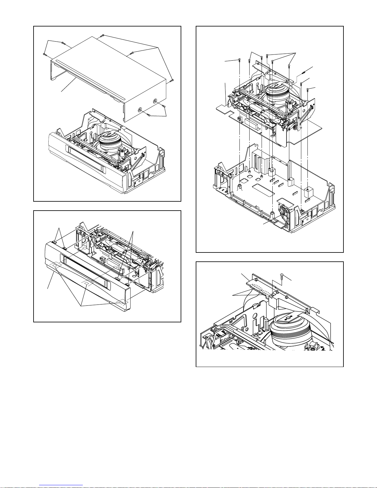
(S-1)
[1] T op Case
(S-1)
(S-1)
Fig. 1
(S-3)
[3]VCR
Chassis Unit
(S-4)
(S-3)
(S-5)
(S-4)
(S-3)
(L-2)
[2] Front
Assembly
(L-1)
(L-2)
(L-3)
Fig. 3
[4] Jack CBA
(S-6)
Desolder
Fig. 2
Fig. 4
1-5-2 HC2C0DC
Page 12
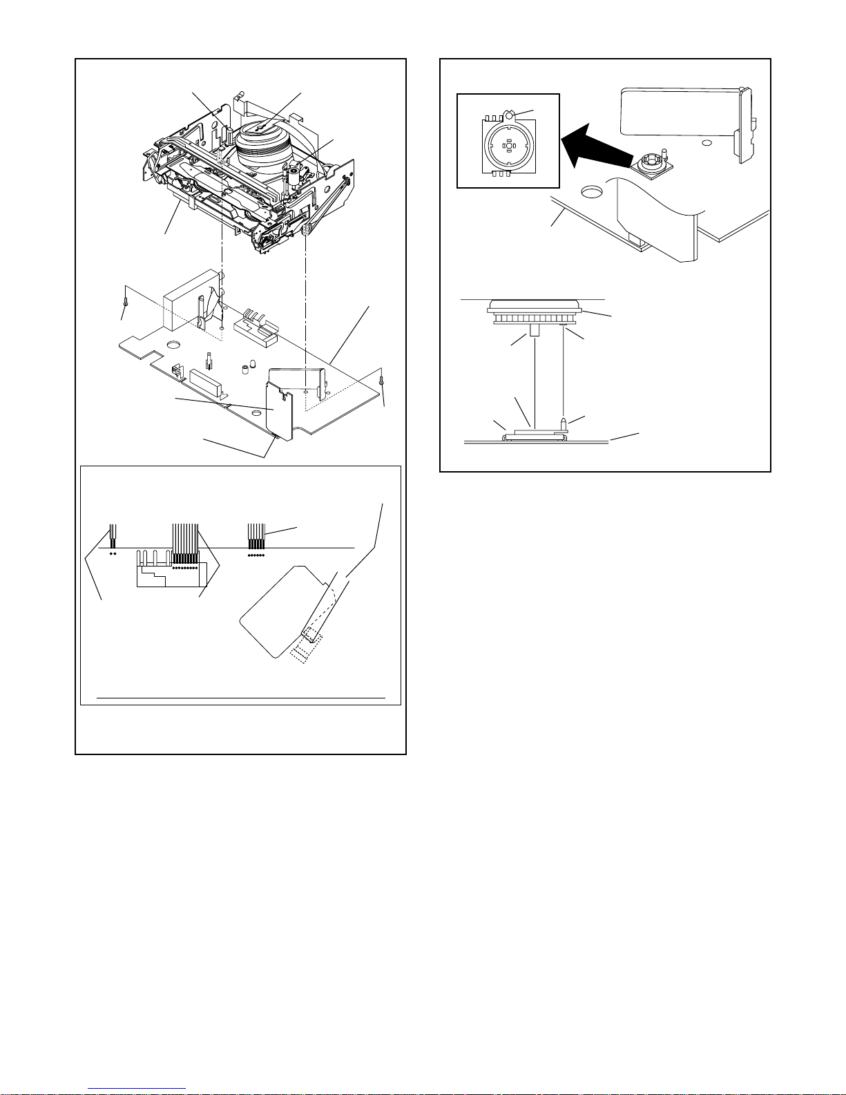
FE Head
Cylinder Assembly
AC Head
Assembly
Pin
SW507
LD-SW
[6] Deck Assembly
(S-7)
[5] Function
CBA
Desolder from
bottom
From
FE Head
Lead with
red stripe
From
Cylinder
Assembly
Lead with
white stripe
From
AC Head
Assembly
[7] Main CBA
From
Capstan Motor
Assembly
Lead with
white stripe
(S-7)
[7] Main CBA
[6] Deck Assembly
Shaft
Hole
LD-SW
Cam Gear
Hole
Pin
[7] Main CBA
Fig. 6
TOP VIEW
Lead connections of Deck Assembly and Main CBA
Fig. 5
1-5-3 HC2C0DC
Page 13
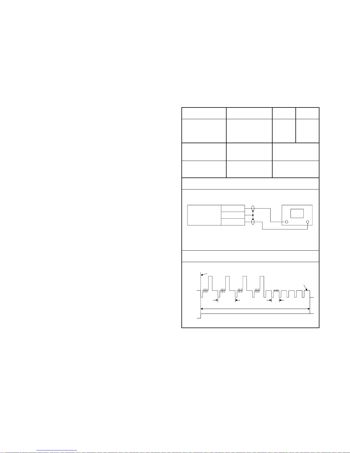
ELECTRICAL ADJUSTMENT INSTRUCTIONS
General Note: "CBA" is an abbreviation for
"Circuit Board Assembly."
NOTE:
1.Electrical adjustments a re required after re placing
circuit component s and certain mechanical parts.
It is important to do these adjustments only afte r
all repairs and replacements have been completed. Also, do not attempt these adjustments
unless the proper equipment is available.
2.To perform these alignment / confirmation procedures, make sure that the tracki ng co ntrol is set in
the center position: P ress eith er "L5??" or "K" button
on the remote control unit first, then the "PLAY"
button (Front Panel only).
Test Equipment Required
1.Oscilloscope: Dual-trace with 10:1 probe,
V-Range: 0.001~50V/Div.,
F-Range: DC~AC-20MHz
2.Alignment Tape (FL6A)
Head Switching Position Adjustment
Purpose:
To determine the Head Switching point during
playback.
Symptom of Misadjustment:
May cause Head Switching noise or ver tical jitter
in the picture.
Test point Adj.Point Mode Input
TP751(V-OUT)
TP502(RF-SW)
GND
Tape
FL6A Oscilloscope
Connections of Measurement Equipment
Main CBA
VR501
(Switching Point)
(MAIN CBA)
Measurement
Equipment
TP751
GND
TP502
PLAY
(SP)
6.5H±1H
(412.7µs±60µs)
Oscilloscope
-----
Spec.
CH1 CH2
Trig. (+)
Figure 1
EXT. Syncronize Trigger Point
V-Sync
CH1
CH2
Reference Notes:
Playback the Alignment tape and adjust VR501 so that
the V-sync front edg e of the CH1 video output waveform is at the 6.5H(412.7µs) delayed position from the
rising edge of the CH2 head switching pulse waveform.
1.0H
Switching Pulse
6.5H
0.5H
1-6-1 HC2C0EA
Page 14
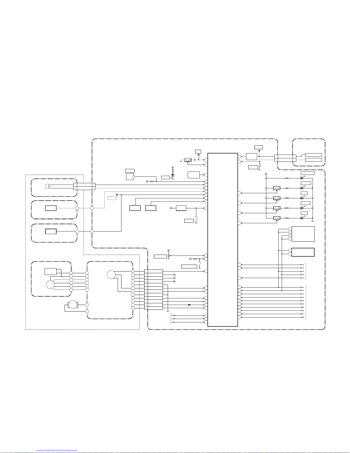
M
M
LOADING
MOTOR
CYLINDER ASSEMBLY CAPSTAN MOTOR
DRUM
MOTOR
PG
SENSOR
CONTROL
HEAD
CL287
5 5CTL(+)
6 6CTL(-)
CL504
AC HEAD ASSEMBLY
MAIN CBA
KEY- 2
C-FG
C-CONT
D-FG
D-PG
ST-S
T-REEL
C-F/R
KEY- 1
REMOCON-IN
CTL(+)
RESET
REC-SAF-SW
PG-DELAY
CTL(-)
D-V SYNC
D-REC-H
RF-SW
H-A-SW
C-ROTA
END-S
14
90
89
94
95
76
87
10
4
80
34
78
2
13
15
18
65
16
31
8
7
RS501
REMOTE
SENSOR
LM-FWD/REV
81
D-CONT77
(DECK ASSEMBLY)
Servo/System Control Block Diagram
BLOCK DIAGRAMS
T-REEL
Q501
RESET
Q503
S-REEL79
SW-POINT
AL+5V
AL+5V
VR501
TIMER+5V
S-REEL
PS503
TP506
I2C-BUS SDA
I2C-BUS SDA
I2C-BUS SCL
A-MUTE-H
A-MUTE-H
H-A-COMP
17
V-ENV
6
P-ON-H
C-POW-SW
P-ON-H
C-POW-SW
P-DOWN-L
67
66
86
P-DOWN-L
C-SYNC
58
SW506
REC-SAFETY
TO
VIDEO BLOCK
TO
AUDIO BLOCK
2 2KEY-2
4 4KEY-1
KEY SWITCH
KEY SWITCH
CL505 CN651
FUNCTION CBA
1-7-1 1-7-2 HC341BLS
SDA
SDA
SCL
SCL
TU701(TUNER UNIT)
IC503 (MEMORY)
72
83
I2C-BUS SCL
D-V SYNC
D-REC-H
RF-SW
H-A-SW
C-ROTA
I2C-BUS SDA
H-A-COMP
V-ENV
C-SYNC
I2C-BUS SCL
71
3
5
SDA
SCL
12
11
LD-SW9
AL+15V/+12V
AL+12V
AL+5V
AL+5V
SW507
P-ON+5V
LD-SW
AL+5V
D502
S-LED
END-S
TO
POWER
SUPPLY
BLOCK
KEY
SWITCH
TP507
S-INH
SW505
CH-UP
M
CAPSTAN
MOTOR
IC501
(SERVO/SYSTEM CONTROL)
AUDIO-SW-2
30
AUDIO-SW-1
AUDIO-SW-2
AUDIO-SW-1
29
5
6
CL502
12 C-F/R
11
AL+15V/+12V
10 AL+12V
9
P-ON+5V
8
GND
7
C-FG
6
C-CONT
5
GND
4
D-FG
3
LM-FWD/REV
2
D-CONT
1
D-PG
SENSOR CBA
SENSOR CBA
END-S
ST-S
Q504
Q505
CTL97
FF/REW-L84
Q502
TP501
CTL
Q562
Q563
Q564
Q565
CAS-LED
TIMER-LED
REC-LED 26
25
24
POWER-LED 23
D565 REC
D564 TIMER
D563 CAS
D562 POWER
D561 STAND-BY
SW508
RESET
Page 15
CYLINDER ASSEMBLY
V(R)-1
V-COM
V(L)-1
CL253
1
2
3
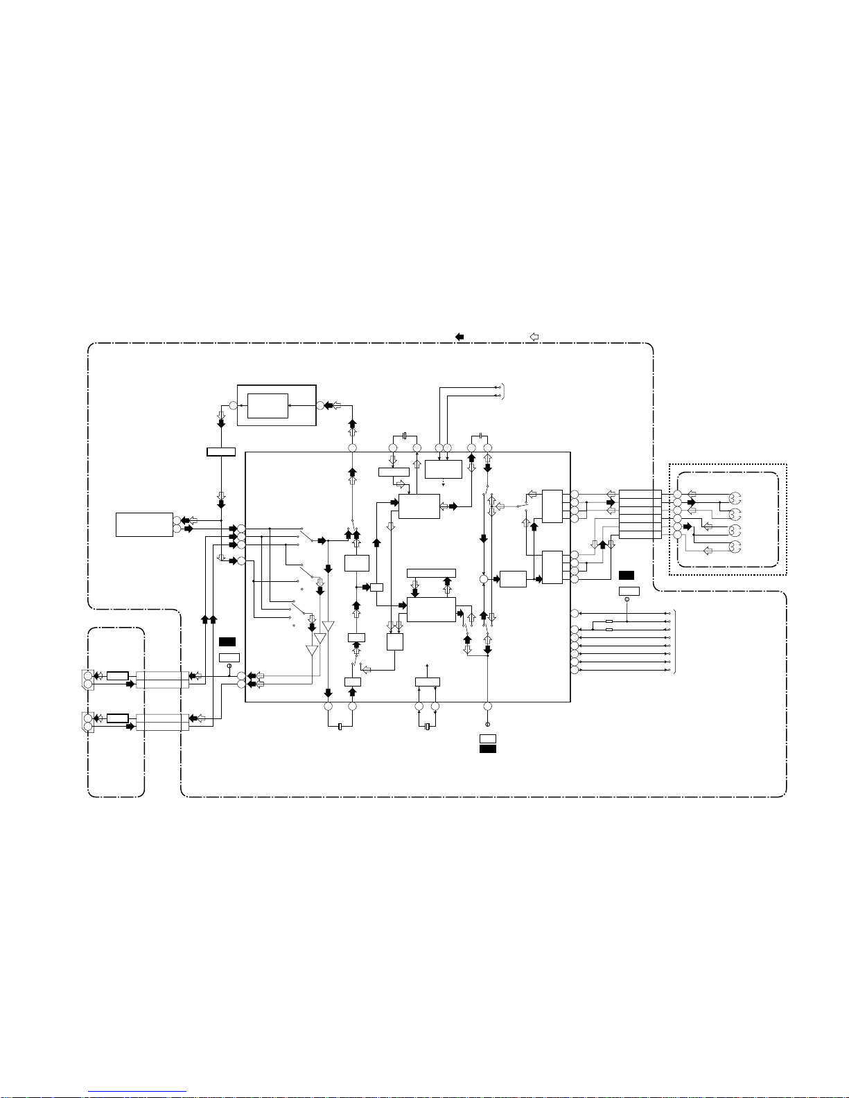
Video Block Diagram
1-7-3 1-7-4 HC341BLV
(DECK ASSEMBLY)
VIDEO (R)-1
HEAD
SP
HEAD
AMP
EP
HEAD
AMP
REC FM
AGC
TO SERVO/SYSTEM
CONTROL BLOCK
C-SYNC
RF-SW
D-REC-H
C-ROTA
D-V-SYNC
H-A-SW
H-A-COMP
V-ENV
LUMINANCE
SIGNAL
PROCESS
CHROMINANCE
SIGNAL
PROCESS
C-SYNC
V-ENV
H-A-COMP
H-A-SW
D-V-SYNC
RF-SW/C-ROTA
VIDEO (L)-1
HEAD
VIDEO (L)-2
HEAD
VIDEO (R)-2
HEAD
V(L)-2
V-COM
V(R)-2
4
5
6
TU701
IC301
(Y/C SIGNAL PROCESS)
IC501 (OSD)
REC-VIDEO SIGNAL PB-VIDEO SIGNAL MODE: SP/REC
SERIAL
DECORDER
V-OUT1
1
V-IN113 3
V-OUT2
1
V-IN2 3
1
3
JACK CBA
48
50
52
56
24
6
50
52
19
20
JK101
V-OUT1
V-IN1
19
20
JK102
CL151
CL152
CL101
CL102
V-OUT2
V-IN2
61
63
96
95
93
94
90
89
88
87
CHARA.
INS.
CCD 1H DELAY
SP
BYPASS
MUTE
PB/EE
IN1
TUNER
IN1
TUNER
MUTE
PB/EE
IN2
IN2
AGC
PR
R
Y
C
P
R P R P
EP
Y. DELAY
Y/C
MIX
+
21
7978
AGC VXO
OSD
CHARACTER
MIX
FBC
1/2
58 59
65
2928
69684643
67
84
83
71
62
70
D-REC-H
80
BUFFER
Q101
BUFFER
Q102
TP751
V-OUT
WF1
TU-VIDEO
VIDEO
MAIN CBA
TP502
RF-SW
WF2
Q351
BUFFER
TO SERVO/SYSTEM
CONTROL BLOCK
I2C BUS SDA
I2C BUS SCL
TP301
X301
4.43MHz
C-PB
WF5
Page 16
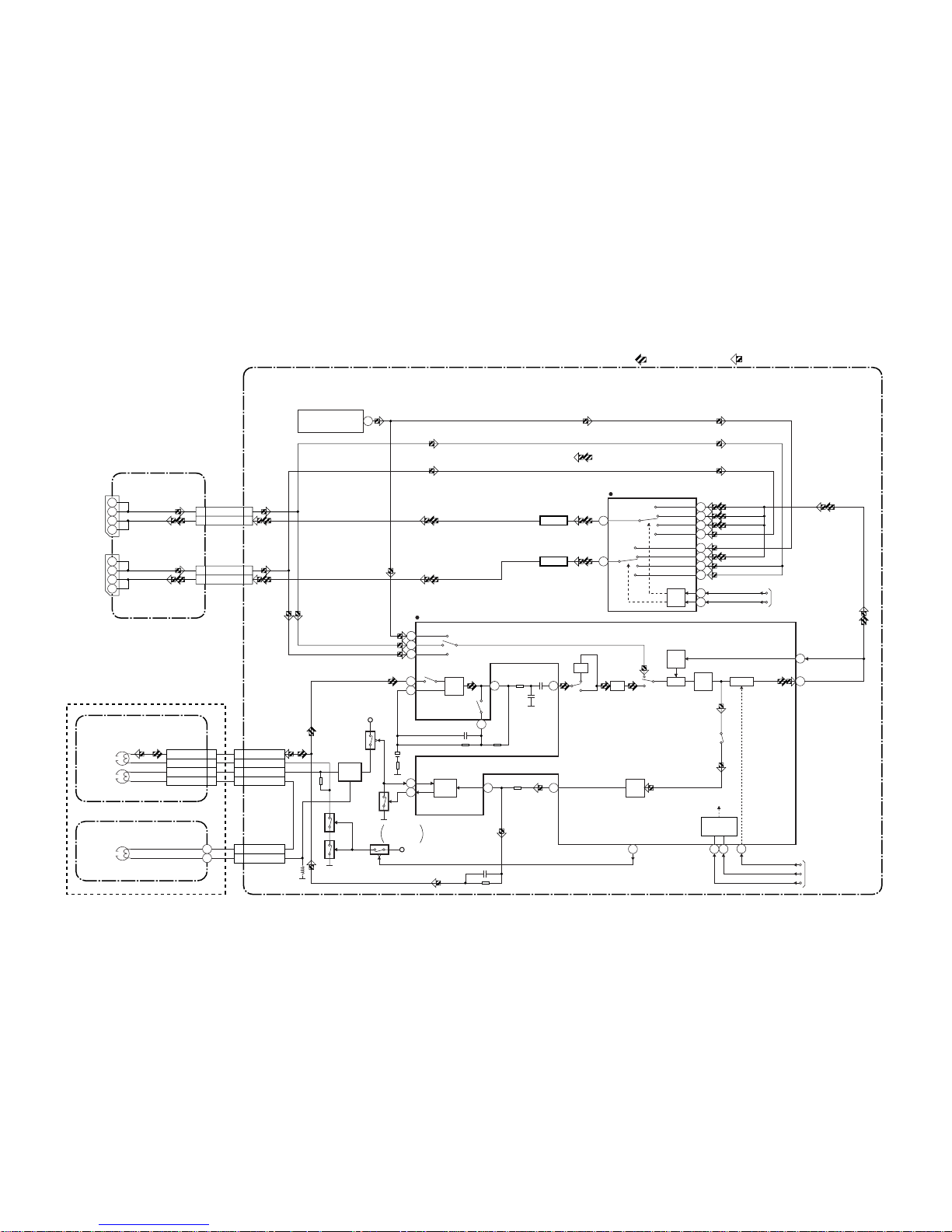
Audio Block Diagram
REC
AMP
100
3
AUTO
BIAS
2
1
+5V
+5V
Q401
Q406
BIAS
OSC
Q402
Q404
(PB=ON)
Q405
(PB=ON)
Q403
SWITCHING
D-REC-OFF
5
EQ
AMP
98
7
LINE
AMP
REC-ON
AUDIO HD-SW
CONTROL
MUTE
11
6
PB-ON
SP/LP-ON
P
R
ALC
DET
ALC
IC301 (AUDIO SIGNAL PROCESS)
4 A-PB/REC
CL504
3 A-COM
1 AE-H
2 AE-H/FE-H
A-PB/REC 4
A-COM 3
AE-H 1
AE-H/FE-H 2
CL287
AUDIO
HEAD
AUDIO
ERASE
HEAD
ACE HEAD ASSEMBLY
FE HEAD
2 FE-H
1 FE-H-GND
CL501
1-7-5 1-7-6 HC341BLA
MAIN CBA
PB-AUDIO SIGNAL REC-AUDIO SIGNAL Mode : SP/REC
71
A-MUTE-H
I2C BUS-SCL
I2C BUS-SDA
TO SERVO/SYSTEM
CONTROL BLOCK
FULL
ERASE
HEAD
68 69
SERIAL
DECODER
(DECK ASSEMBLY)
12
16
INV
ATT
TU701
SW
CTL
IC151 (SWITCHING)
PB/EE
PB/EE
PB/EE
PB/EE
TUNER
TU-AUDIO
IN2
IN1
IN1
AUDIO-SW-1
AUDIO-SW-2
TO SERVO/SYSTEM
CONTROL BLOCK
A-IN1
A-OUT1
8
6
JACK CBA
JK101
A-IN1(R)
A-IN1(L)
2
6
1
3
CL101
A-OUT1(R)
A-OUT1(L)
A-IN2
A-OUT2
8
6
8
6
8
6
JK102
A-IN2(R)
A-IN2(L)
2
6
1
3
CL102
CL151
CL152
A-OUT2(R)
A-OUT2(L)
21
1
5
2
4
12
14
15
11
10
9
3
13
TUNER
IN2
IN1
15
13
17
BUFFER
Q151
BUFFER
Q152
Page 17
2
4
16
6
7
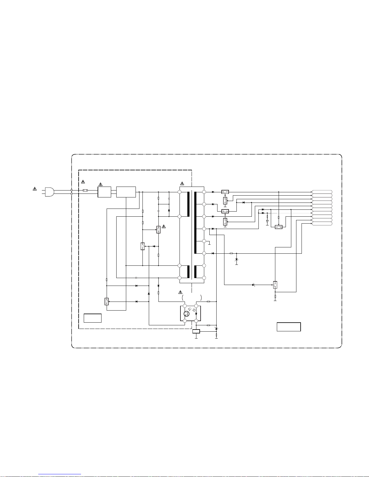
Power Supply Block Diagram
CAUTION
FOR CONTINUED PROTECTION AGAINST FIRE HAZARD,
REPLACE ONLY WITH THE SAME TYPE T1.6AL/250V FUSE.
NOTE :
The voltage for parts in hot circuit is measured using
hot GND as a common terminal.
CAUTION !
Fixed voltage (or Auto voltage selectable ) power supply circuit is used in this unit.
If Main Fuse (F001) is blown, check to see that all components in the power supply
circuit are not defective before you connect the AC plug to the AC power supply.
Otherwise it may cause some components in the power supply circuit to fail.
HC341BLP
1-7-7 1-7-8
COLD
MAIN CBA
HOT CIRCUIT. BE CAREFUL.
HOT
IC001
ERROR
VOLTAGE DET
Q002
Q003
Q001
F001
L003
LINE
FILTER
BRIDGE
RECTIFIER
D001 - D004
1
2
3
4
Q004
(SHUNT REGULATOR)
REG
AC001
T001
P-ON+44V
12
P-ON-H
AL+15V/+12V
AL+12V
C-POW-SW
AL+5V
TIMER+5V
P-ON+5V
P-DOWN-L
AL-5V
Q051
Q054
Q056
Q052
Q057
Q058
13
15
14
11
17
18
T1.6A L 250V
Page 18
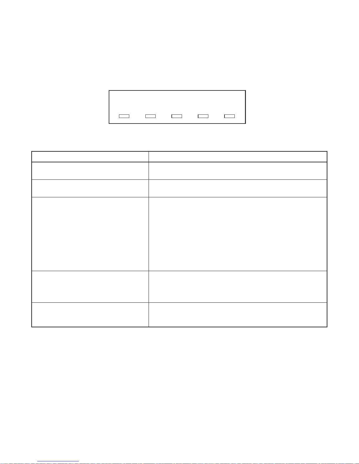
FUNCTION INDICATOR SYMBOLS
Note:
The following symb ols wi ll ap pea r on t he i nd ic ato r panel to indicate the c ur rent mode or operatio n of the VCR.
On-screen modes will also be momentarily displayed on the tv screen when you press the operation buttons.
Display panel
RECFUNCTIONSTANDBY TAPE IN TIMER
" H "= LED Light on, " L "= LED Light off
Led Mode Indicator Active
STANDBY Power on = " H "
Power off = " L "
FUNCTION VCR mode = " H "
TV mode = " L "
TAPE IN
1. When reel and capstan mechanism is
not functioning correctly
2. When tape loading mechanism is not
functioning correctly
3. When cassette loading mechanism is
not functioning correctly
4. When the drum is not working properly
TIMER Timer stand by = " H "
REC REC mode = " H "
Cassette in = " H "
Cassette out = " L "
Cassette in
Cassette in
Cassette in
Cassette in
One touch recording = " H "
Timer recording = " H "
General mode = " L "
REC pause
General mode = " L "
Blinks at 0.8Hz interval
Blinks at 1.6Hz interval
Blinks at 3.2Hz interval
Blinks at 6.4Hz interval
Blinks at 0.8Hz interval
1-7-9 HC341FIS
Page 19
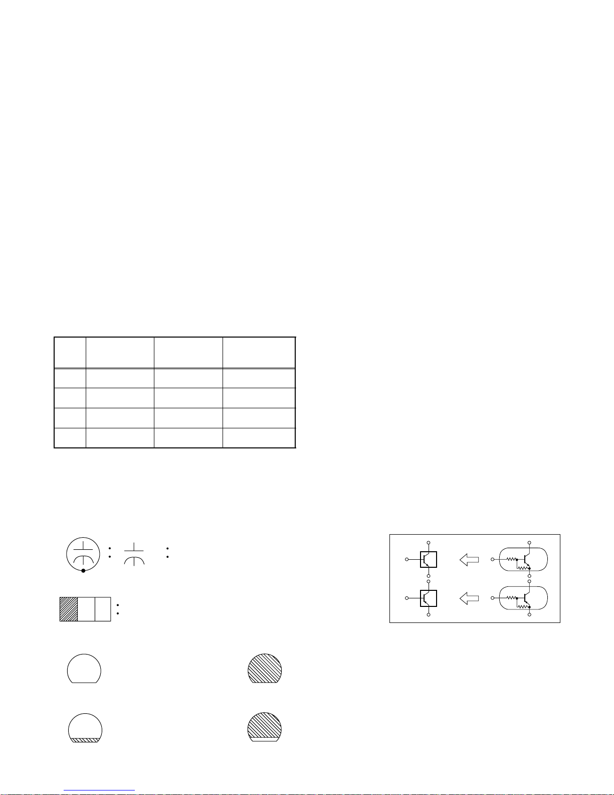
SCHEMATIC DIAGRAMS / CBA’S AND TEST POINTS
Standard Notes
WARNING
Many electrical and mechanical parts in this chassis
have special characteristics. These characteristics
often pass unnoticed and the protection afforded by
them cannot necessarily be obtained by using replacement components rated for higher voltage, wattage,
etc. Replacement p arts that ha ve these special safety
characteristics are identified in this manual and its
supplements; ele ctrical components having such features are identified by the mark " ! " in the schematic
diagram and the parts list. Before replacing any of
these components, read the parts list in this manual
carefully. The use of substit ute replaceme nt parts that
do not have the same s afety character istics as specified in the parts list may create shock, fire, or other
hazards.
Capacitor Temperature Markings
Mark
Capacity
change rate
Standard
temperature
Temperature
range
Notes:
1. Do not use the part number shown on these dr awings for ordering. The correct part number is shown
in the parts list, and may be slightly different or
amended since these drawings were prepared.
2. All resistance values are indicated in ohms
3
(K=10
3. Resistor wattages are 1/4W or 1/6W unless otherwise specified.
4. All capacitance va lue s ar e indicated in µF
(P=10
5. All voltages are DC voltages unless otherwise
specified.
6. Electrical parts such as capacitors, connectors,
diodes, IC’s, transistors, resistors, switches, and
fuses are identi fied by four di gits. The fir st two digits are not shown for each component. In each
block of the diagram, there is a note such as shown
below to indicate these abbreviated two digits.
, M=106).
-6
µF).
(B)
(F) +30 - 80% 20°C -25~+85°C
(SR)
(Z) +30 - 80% 20°C -10~+70°C
Capacitors and transistors are represented by the following symbols.
±
±
10%
15%
20°C -25~+85°C
20°C -25~+85°C
CBA Symbols
(Top View) (Bottom View)
+
Electrolytic Capacitor
(Bottom View)
Transistor or Digital Transistor
E C B
(Top View)
(Top View)
Schematic Diagram Symbols
Digital Transistor
NPN Transistor
E C B
(Top View)
NPN Digital Transistor
E C B
PNP Transistor
E C B
(Top View)
PNP Digital
Transistor
E C B
1-8-1 SCPA1
Page 20
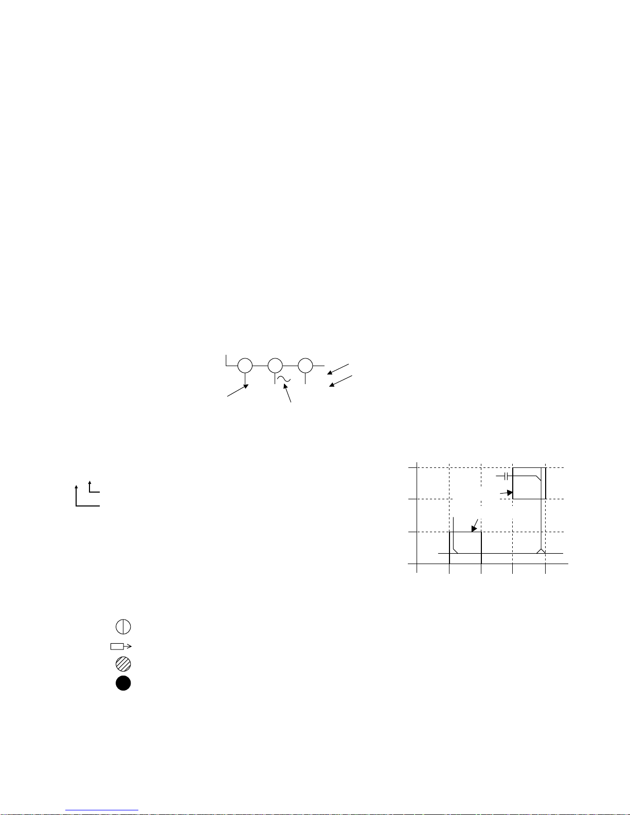
LIST OF CAUTION, NOTES, AND SYMBOLS USED IN THE SCHEMATIC DIAGRAMS ON THE FOLLOWING
PAGES:
1.
CAUTION:
FOR CONTINUED PROTECTION AGAINST FIRE HAZARD, REPLACE ONLY WITH THE SAME TYPE FUSE.
2.
CAUTION:
Fixed Voltage (or Auto voltage selectable) power supply circuit is used in this unit.
If Main Fuse (F001) is blown, first check to see that all components in the power supply circuit are not defective
before you connect the AC plug to the AC power supply. Otherwise it may cause some components in the
power supply circuit to fail.
3.
Note:
(1) Do not use the part number shown on the drawings for ordering. The correct part number is shown in the parts
list, and may be slightly different or amended since the drawings were prepared.
(2) To maintain origi nal function and reliability of rep aired units, use only original replacement parts which are
listed with their part numbers in the parts list section of the service manual.
4. Wire Connectors
(1) Prefix symbol "CN" means "connector" (can disconnect and reconnect).
(2) Prefix symbol "CL" means "wire-solder holes of the PCB" (wire is soldered directly).
5. Mode: SP/REC
6. Voltage indications for PLAY and REC modes on the schematics are as shown below:
Unit: Volts
The same voltage for
both PLAY & REC modes
7. How to read converged lines
1-D3
Distinction Area
Line Number
(1 to 3 digits)
Examples:
1. "1-D3" means that line number "1" goes to area "D3".
2. "1-B1" means that line number "1" goes to area "B1".
8. Test Point Information
: Indicates a test point with a jumper wire across a hole in the PCB.
: Used to indicate a test point with a component lead on foil side.
5.0
231
5.0
PLAY mode
REC mode
(2.5)
Indicates that the voltage
is not consistent here.
3
AREA D3
2
1
AREA B1
1-D3
ABCD
1-B1
: Used to indicate a test point with no test pin.
: Used to indicate a test point with a test pin.
1-8-2 SCRK05
Page 21
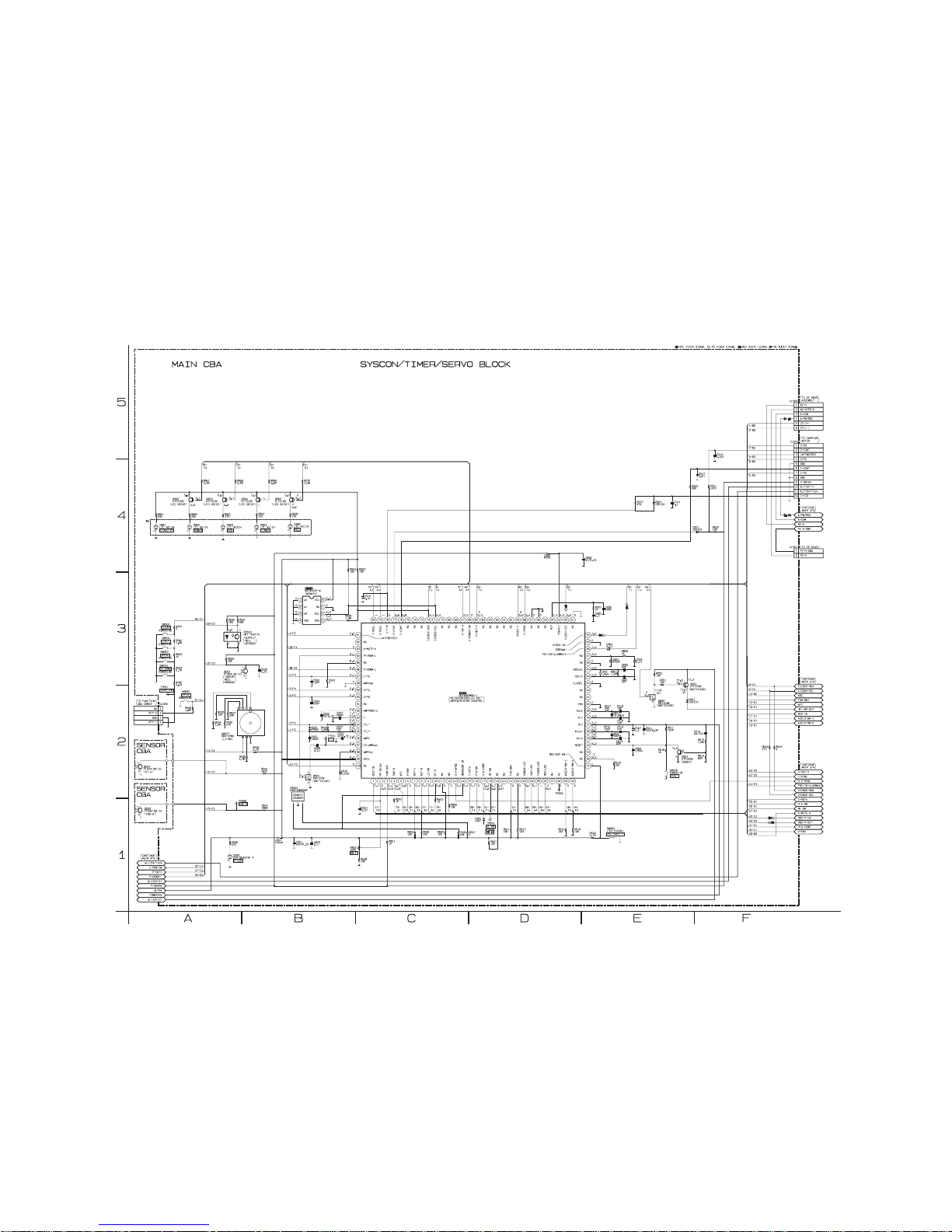
1-8-3 1-8-4 1-8-5
HC341SCM1
Main 1/4 Schematic Diagram
Note:
When it is necessary to replace one or more of the following Diodes,
all five should be replaced: D561, D562, D563, D564, D565.
*
1
Page 22
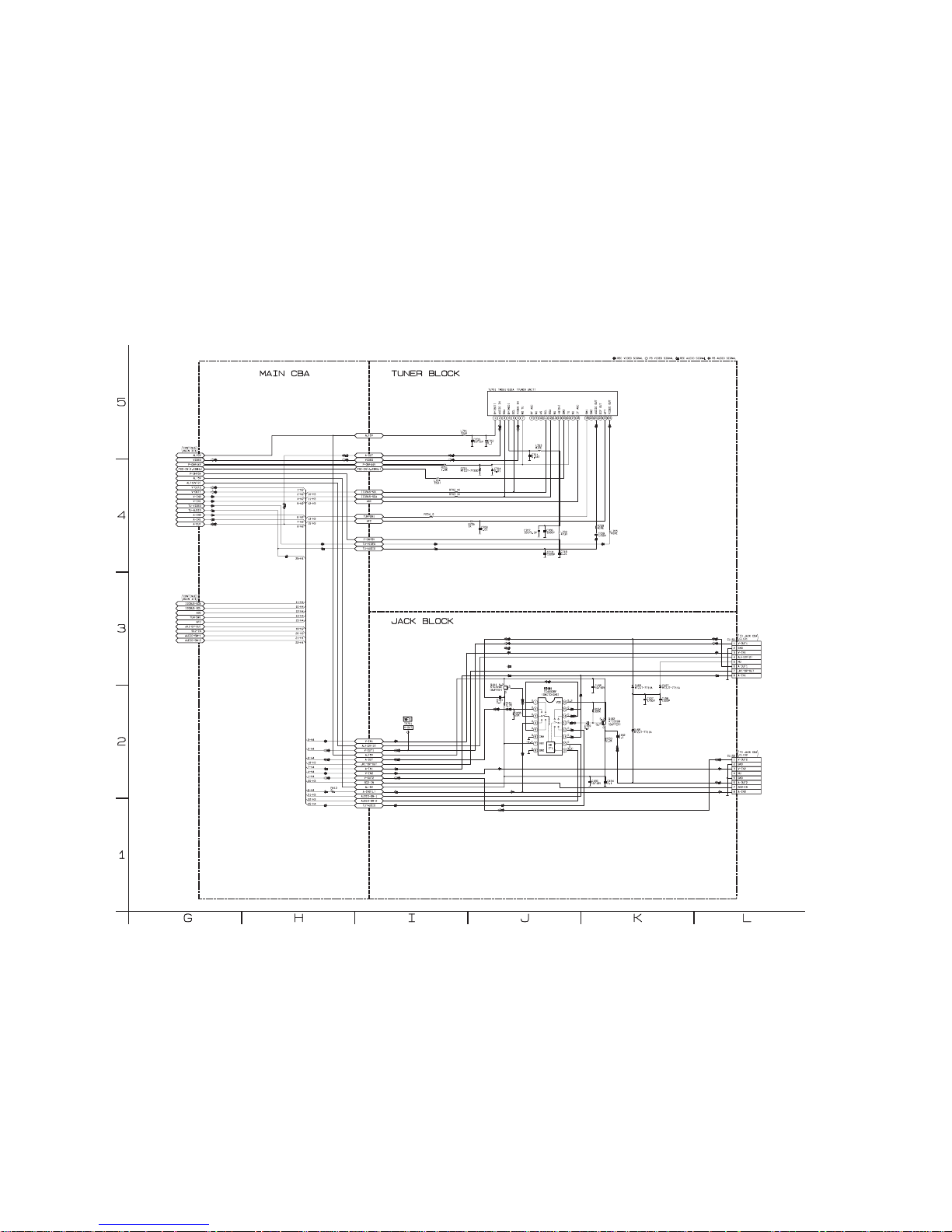
1-8-6 1-8-7 1-8-8 HC341SCM2
Main 2/4 Schematic Diagram
Page 23
1-8-9
1-8-10
1-8-11
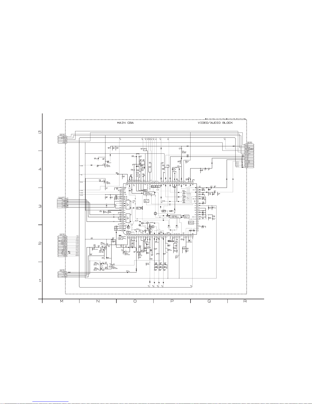
HC341SCM3
Main 3/4 Schematic Diagram
Page 24
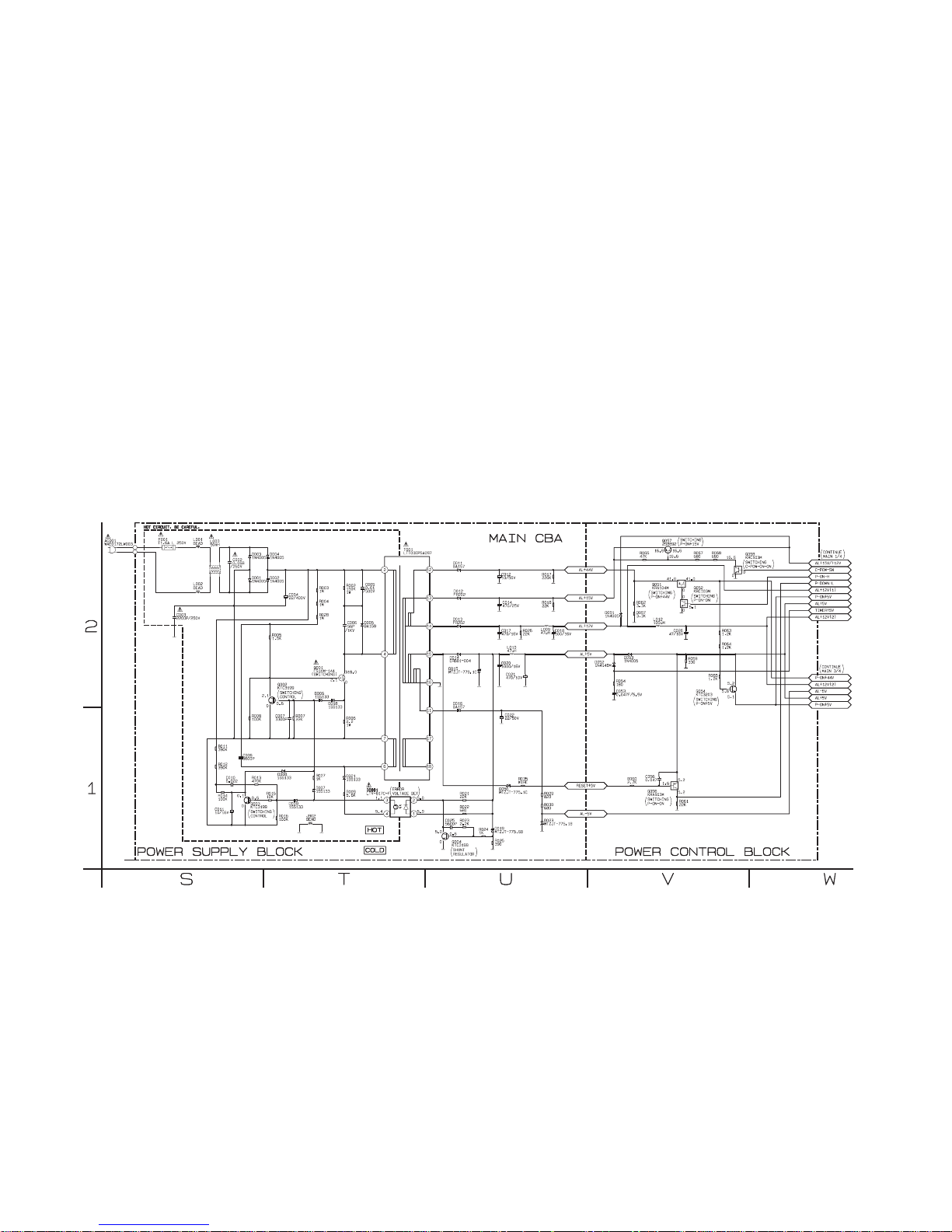
1-8-12
1-8-13 1-8-14
HC341SCM4
Main 4/4 Schematic Diagram
NOTE :
THE VOLTAGE FOR PARTS IN HOT CIRCUIT IS MEASURED USING
HOT GND AS A COMMON TERMINAL.
CAUTION
FOR CONTINUED PROTECTION AGAINST FIRE HAZARD,
REPLACE ONLY WITH THE SAME TYPE FUSE.
CAUTION !
Fixed voltage (or Auto voltage selectable ) power supply circuit is used in this unit.
If Main Fuse (F001) is blown, check to see that all components in the power supply
circuit are not defective before you connect the AC plug to the AC power supply.
Otherwise it may cause some components in the power supply circuit to fail.
Page 25
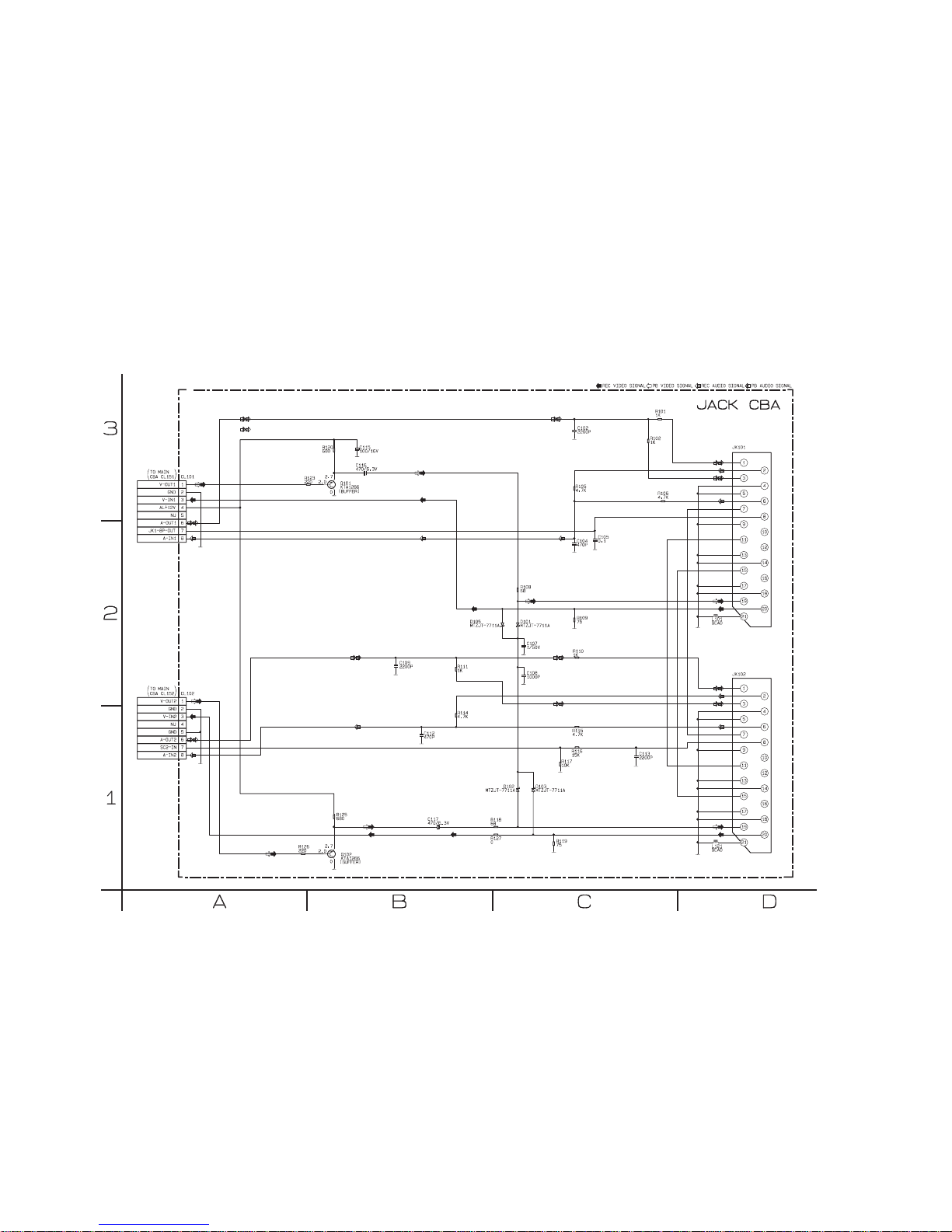
Jack Schematic Diagram
1-8-15
1-8-16
HC341SCJ
Page 26
1-8-17
1-8-18
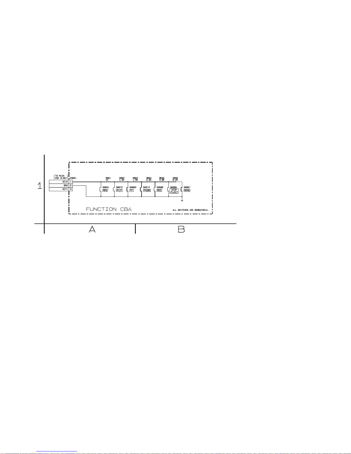
Function Schematic Diagram
HC341SCF
Page 27
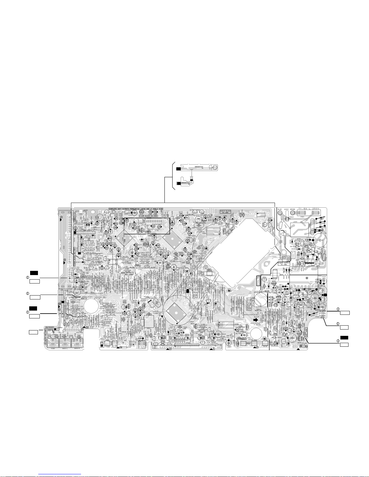
VR501
SW-P
WF2
TP502
RF-SW
TP501
CTL
TP507
S-INH
WF5
TP301
C-PB
TP506
END-S
WF1
TP751
V-OUT
1-8-19
BHC400F01018-A
Main CBA Top View
BHB300F01011-A
BHB300F01011-B
Sensor CBA Top View
1-8-20 1-8-21
CAUTION !
Fixed voltage power supply circuit is used in this unit.
If Main Fuse (F001) is blown, check to see that all components in the power supply
circuit are not defective before you connect the AC plug to the AC power supply.
Otherwise it may cause some components in the power supply circuit to fail.
BECAUSE A HOT CHASSIS GROUND IS PRESENT IN THE POWER
SUPPLY CIRCUIT , AN ISOLATION TRANSFORMER MUST BE USED.
ALSO , IN ORDER TO HAVE THE ABILITY TO INCREASE THE INPUT
SLOWLY , WHEN TROUBLESHOOTING THIS TYPE POWER SUPPLY
CIRCUIT , A VARIABLE ISOLATION TRANSFORMER IS REQUIRED.
NOTE :
The voltage for parts in hot circuit is measured using
hot GND as a common terminal.
CAUTION
FOR CONTINUED PROTECTION AGAINST FIRE HAZARD,
REPLACE ONLY WITH THE SAME TYPE FUSE.
Page 28
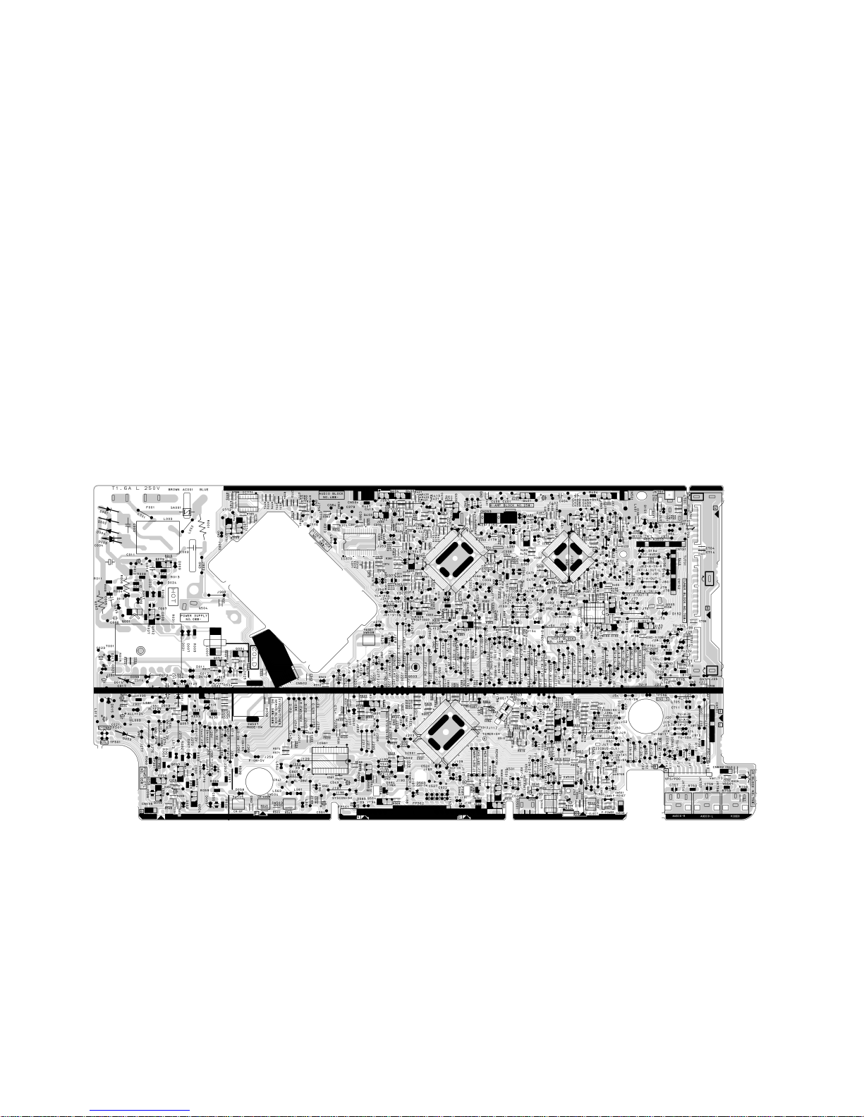
1-8-22
1-8-23
1-8-24
BHC400F01018-A
Main CBA Bottom View
CAUTION !
Fixed voltage power supply circuit is used in this unit.
If Main Fuse (F001) is blown, check to see that all components in the power supply
circuit are not defective before you connect the AC plug to the AC power supply.
Otherwise it may cause some components in the power supply circuit to fail.
BECAUSE A HOT CHASSIS GROUND IS PRESENT IN THE POWER
SUPPLY CIRCUIT , AN ISOLATION TRANSFORMER MUST BE USED.
ALSO , IN ORDER TO HAVE THE ABILITY TO INCREASE THE INPUT
SLOWLY , WHEN TROUBLESHOOTING THIS TYPE POWER SUPPLY
CIRCUIT , A VARIABLE ISOLATION TRANSFORMER IS REQUIRED.
NOTE :
The voltage for parts in hot circuit is measured using
hot GND as a common terminal.
CAUTION
FOR CONTINUED PROTECTION AGAINST FIRE HAZARD,
REPLACE ONLY WITH THE SAME TYPE FUSE.
Page 29
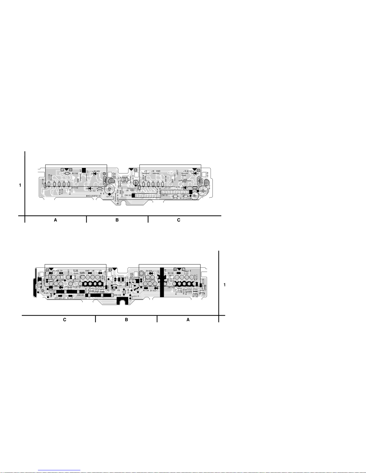
Jack CBA Top View
Jack CBA Bottom View
BHC400F01018-E
1-8-25
1-8-26
Page 30
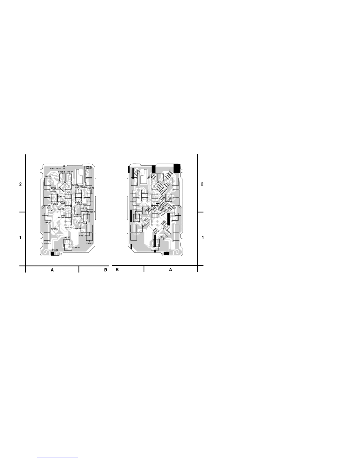
Function CBA Top View Function CBA Bottom View
1-8-27
1-8-28
BHC400F01018-B
Page 31
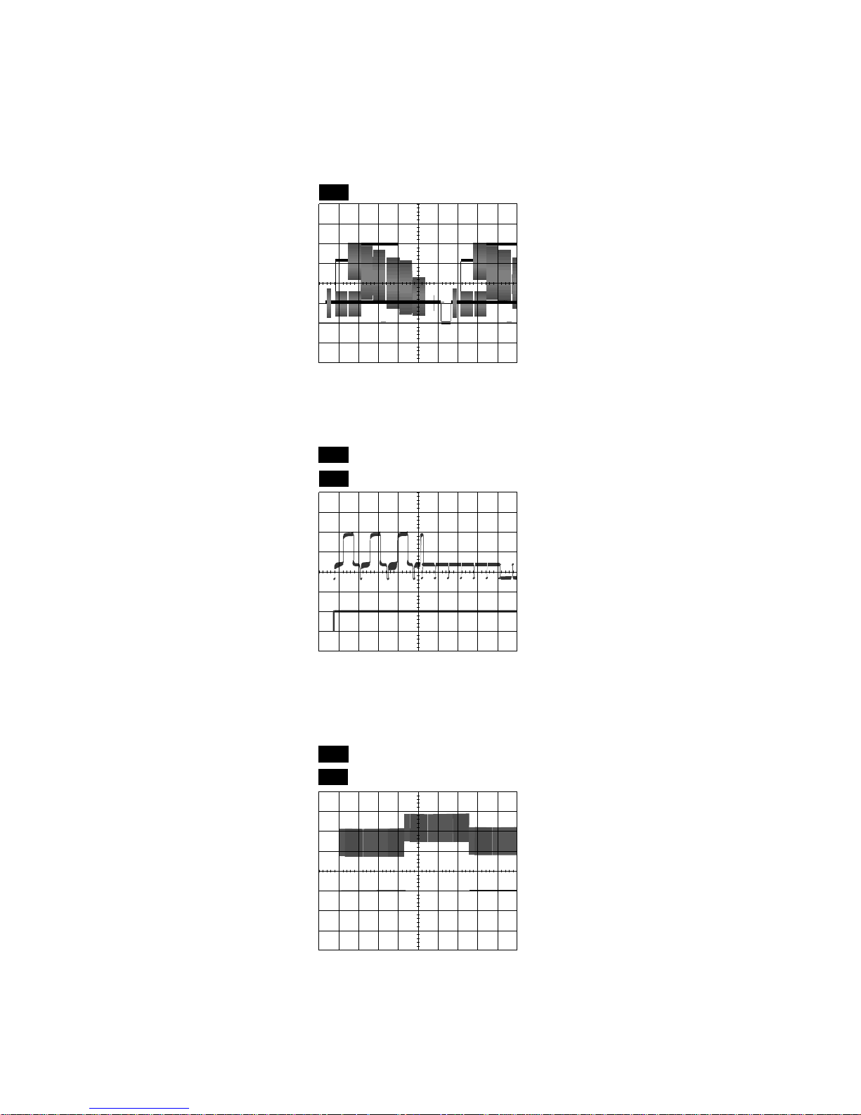
1-9-1 U25WFPAL
WF1
V-OUT E-E
10usec 50mV x 10
WAVEFORMS
(TP751 of Main CBA)
WF1
UPPER
WF2
LOWER
V-OUT 0.1V x 10
RF-SW 0.5V x 10
50usec
(TP751 of Main CBA)
(TP302 of Main CBA)
WF5
C-PB 10mV x 10
RF-SW 0.5V x 10
5msec
UPPER
LOWER
WF2
(TP302 of Main CBA)
(TP301 of Main CBA)
Page 32
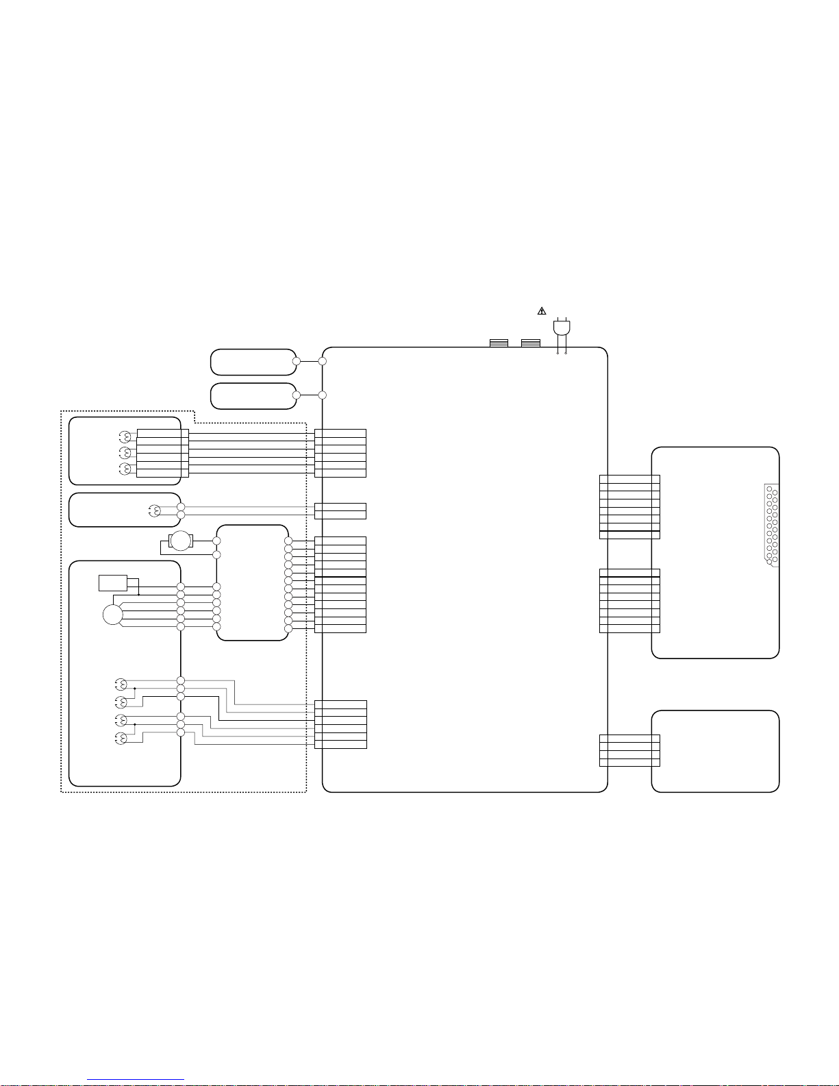
WIRING DIAGRAM
HC341WI1-10-1 1-10-2
GND
1 V-OUT1
2
AL+12V(2)
3 V-IN1
4
NU5
A-OUT
6
JK1-8P-OUT
7
A-IN18
1
2
3
4
5
6
7
8
CL151
CL101
KEY2
GND
2
3
2
NU
1 1
3
KEY1
4 4
CN651CL505
GND
1 V-OUT2
2
NU
3 V-IN2
4
GND5
A-OUT
6
SC2-IN
7
A-IN28
1
2
3
4
5
6
7
8
CL152 CL102
AC CORD
ANT-IN ANT-OUT
FUNCTION CBA
1
2
3
4
5
6
7
8
9
10
11
12
13
14
15
16
17
18
19
20
21
JACK CBA
AC HEAD ASSEMBLY
AUDIO HEAD
AUDIO
ERASE HEAD
CONTROL HEAD
AE-H
AE-H/FE-H
A-COM
A-PB/REC
CTL(+)
CTL(-)
6
5
4
3
2
1
CL287
MLOADING
MOTOR
CYLINDER ASSEMBLY
AE-H
1
AE-H/FE-H2
A-COM3
A-PB/REC4
CTL(+)5
CTL(-)
6
V-COM5
V(R)-26
V(R)-11
V-COM2
V(L)-2
3 V(L)-1
4
AL+15V/+12V
12 C-F/R
11
P-ON+5V
10 AL+12V(1)
9
GND8
C-FG
7
C-CONT
6
GND5
D-FG4
LM-FWD/REV
3
D-CONT
2
D-PG1
FE-H2
FE-H GND1
CL501
CL502
CL504
CL253
CAPSTAN MOTOR
FULL
ERASE HEAD
FE HEAD
VIDEO
(R)1 HEAD
VIDEO
(L)1 HEAD
VIDEO
(L)2 HEAD
VIDEO
(R)2 HEAD
M
DRUM
MOTOR
PG
SENSOR
(DECK ASSEMBLY)
SENSOR CBA
(BHB300F01011)
SENSOR CBA
(BHB300F01011)
MAIN CBA
(BHC400F01018B)
(BHC400F01018E)
(BHC400F01018A)
JK101,102
Page 33
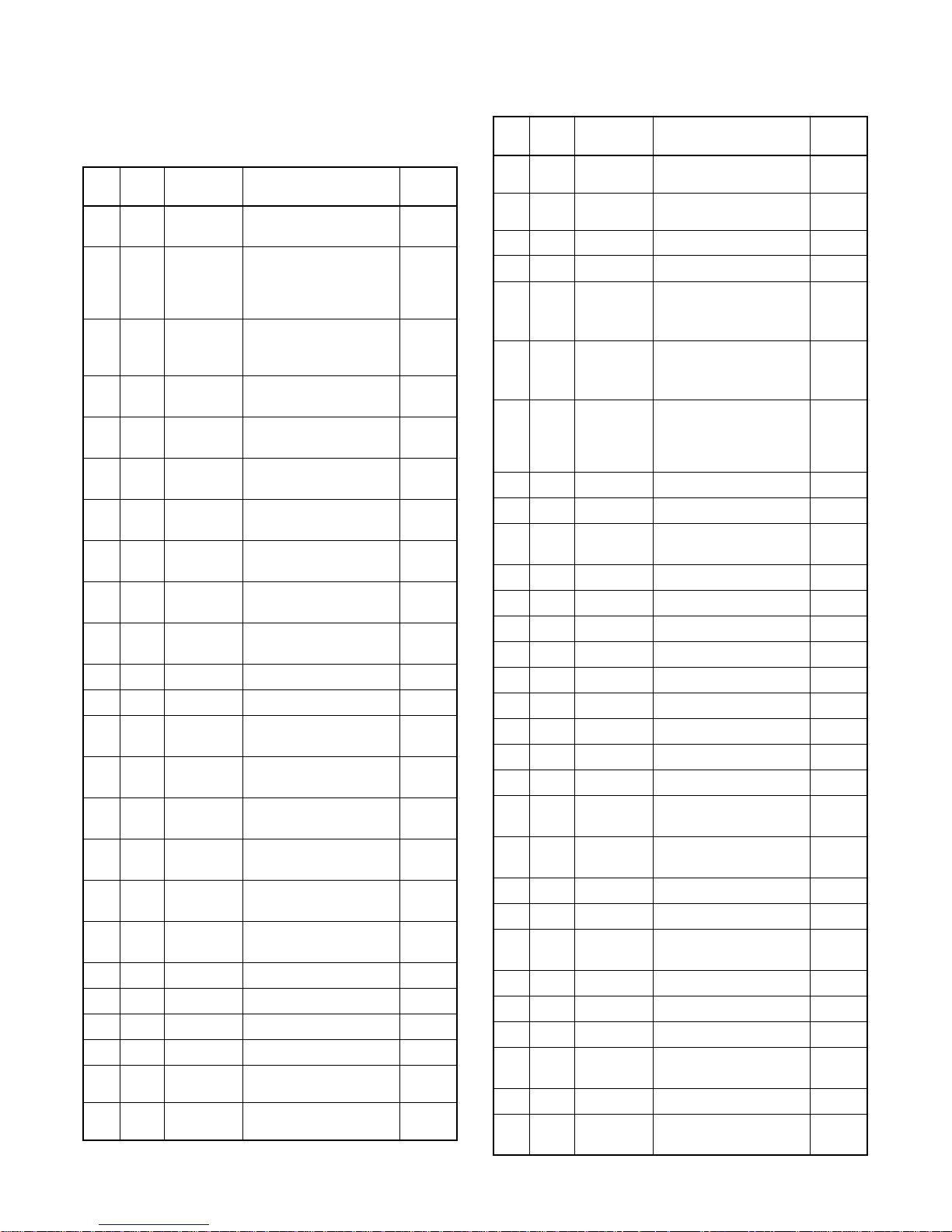
IC PIN FUNCTION DESCRIPTIONS
IC501( SERVO / SYSTEM CONTROL IC )
“H” ≥ 4.5V, “L” ≤ 1.0V
Pin
IN/
No.
OUT
1IN
2IN
3IN
4IN
5IN
6IN
7IN
8IN
9IN
10 IN
11 -
12 13 OUT
14 IN
15 OUT
16 OUT
17 IN
18 OUT
19 -
20 21 22 -
23 OUT
24 OUT CAS LED
Signal
Name
SC2-IN
PGDELAY
POWSAF
END-S
AFC
V-ENV
KEY-1
KEY-2
LD-SW
ST-S
N.U. Not Used
N.U. Not Used
D-V-
SYNC
REMOCO
N-IN
C-ROTA
H-A-SW
H-A-
COMP
RF-SW
N.U. Not Used
N.U. Not Used
N.U. Not Used
N.U. Not Used
POWER
LED
Function
Input Signal from
Pin 8 of SCART2
Video Head
Switching Puls e
Signal Adjusted
Voltage
P-ON Power
Detection Input
Signal
Tape End Position
Detect Signal
Automatic Frequency
Control Signal
Video Envelope
Comparator Signal
Key Scan Input
Signal 1
Key Scan Input
Signal 2
Deck Mode Position
Detector Signal
Tape Start Position
Detector Signal
Dummy V-sync
Output
Remote
Control Sensor
Color Phase Rotary
Changeover SIgnal
Video Head Amp
Switching Puls e
Head Amp
Comparator Signal
Video Head
Switching Puls e
“STANDBY” LED Signal Output
“TAPE IN” LED Signal Output
Active
Level
L/Hi-z
A/D
A/D
A/D
A/D
A/D
A/D
A/D
A/D
A/D
H/Hi-z
H/L
H/L
H/L
H/L
H/L
H/L
Pin
IN/
No.
OUT
25 OUT
26 OUT REC LED
27 28 -
29 OUT
30 OUT
31 IN
32 33 -
34 IN
35 IN
36 OUT
37 38 IN
-
-
L
-
-
-
-
39 OUT
40 41 42 43 IN
44 IN
45 OUT
46 -
47 48 IN
49 -
50 IN
51 -
52 OUT
53 54 -
Signal
Name
TIMER
LED
N.U. Not Used
N.U. Not Used
AUDIOSW1
AUDIOSW2
REC-SAF
N.U. Not Used
N.U. Not Used
RESET
XC-IN Sub Clock
XC-OUT Sub Clock
Vcc Vcc
X-IN Main Clock Input
X-OUT Main Clock Input
Vss Vss(GND)
N.U. Not Used
N.U. Not Used
CLKSEL Clock Select (GND)
IN
OSC
OUT
OSC
N.U. Not Used
N.U. Not Used
FSC-IN
[4.43MHz]
OSDVss OSDVss
VIDEO-IN Video Signal Input
N.U. Not Used
VIDEO-
OUT
OSDVcc OSDVcc
HLF
Function
“TIMER” LED Signal
Output
“REC” LED Signal
Output
Audio Input/Output
Switching Control
Signal 1 (Mono)
Audio Input/Output
Switching Control
Signal 2 (Mono)
Recording Safety SW
Detect (With Record
tab="L"/With out
Record tab="H")
System Reset
Signal (Reset=”L”)
Clock Input
for letter size
Clock Output for letter
size
4.43MHz Clock Input
Video Signal Output
LPF Connected
Terminal (Slicer)
Active
Level
H/L
H/L
-
-
Z/L
Z/L
H
-
-
L
-
-
-
-
-
-
-
-
L
-
-
-
-
-
-
-
-
-
-
-
1-11-1 HC341PIN
Page 34
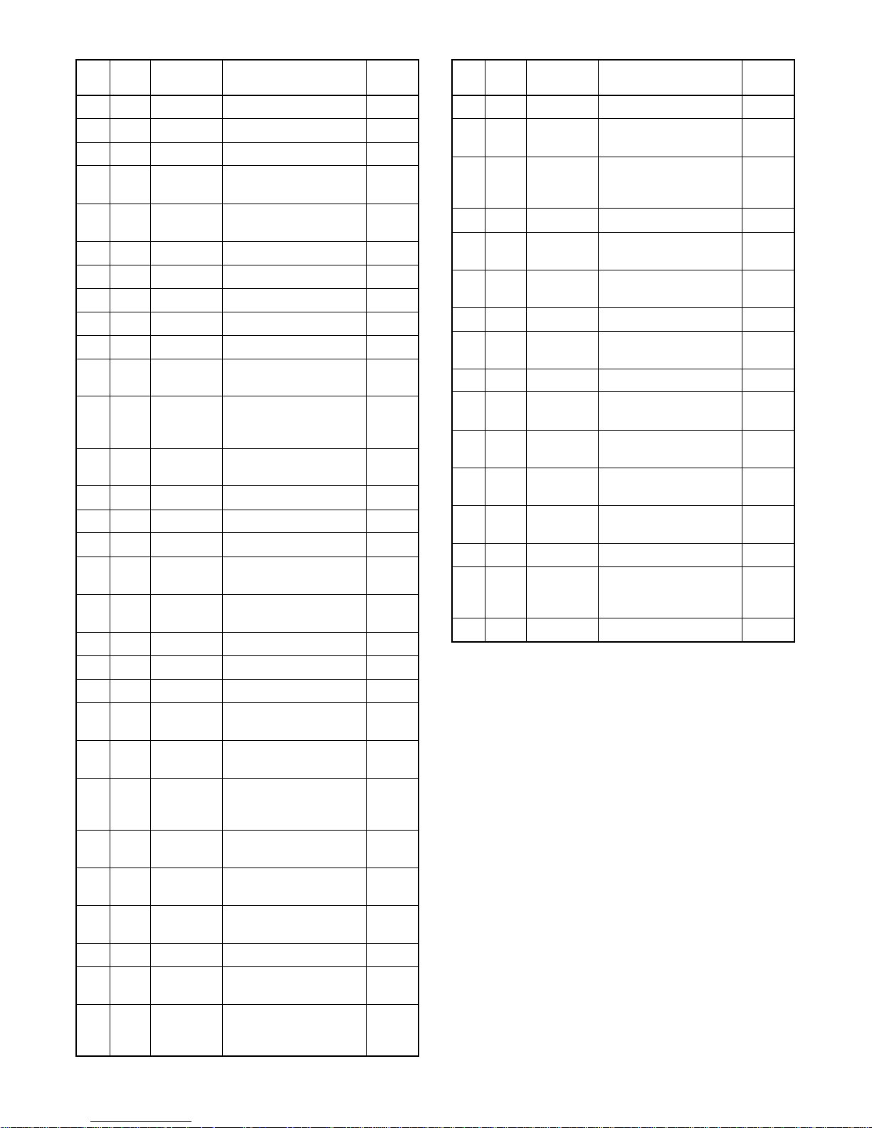
Pin
IN/
No.
OUT
55 56 57 -
58 IN
59 OUT
60 -
61 62 63 64 -
65 OUT
66 OUT
67 IN
68 -
69 70 -
71 OUT
IN/
72
OUT
73 74 75 -
76 OUT
77 OUT
78 OUT
79 IN
80 IN
81 OUT
82 83 OUT
84 OUT
Signal
Name
Function
N.U. Not Used
N.U. Not Used
N.U. Not Used
C-SYNC
8POUT-1
Composite
Synchronized Pulse
SCART 1 8Pin
Output Control Signal
N.U. Not Used
N.U. Not Used
N.U. Not Used
N.U. Not Used
N.U. Not Used
D-REC-H
C-
POWERSW
P-ON-H
Delayed Record
Signal
Capstan Power
Switching Puls e
Power On Signal at
High
N.U. Not Used
N.U. Not Used
N.U. Not Used
IIC BUS-
SCL
IIC BUS-
SDA
IIC BUS Control
Clock
IIC BUS Control Data
N.U. Not Used
N.U. Not Used
N.U. Not Used
C-CONT
D-CONT
Capstan Motor
Control Signal
Drum Motor Control
Signal
Capstan Motor FWD/
C-F/R
REV Control Signal
(FWD=”L”/REV=”H”)
S-REEL
T-REEL
LM-FWD/
REV
Supply Reel
Rotation Signal
Take Up Reel
Rotation Signal
Loading Motor
Control Signal
N.U. Not Used
A-MUTE-H Audio Mute Control
Signal (Mute = “H”)
FF/REW-
L
CTL Amp Gain
Switching Signal (FF/
REW=”L”)
Active
Level
-
-
-
PULSE
H/L
-
-
-
-
-
L
L/Hi-z
H
-
-
-
H/L
H/L
-
-
-
PWM
PWM
H/L
PULSE
PULSE
H/L/
Hi-z
-
H
L
Pin
No.
OUT
85 86 IN
IN/
Signal
Name
Function
N.U. Not Used
P-DOWN-LPower Voltage Down
Detector Signal
Capstan Motor
87 IN
C-FG
Rotation Detection
Pulse
88 89 IN
90 IN
91 92 93 94 OUT
95 OUT
96 -
97 98 -
AMPVss AMPVss (GND)
D-FG
D-PG
Drum Motor Rotation
Detection Pulse
Drum Motor Pulse
Generator
N.U. Not Used
AMPVRE
F
IN
V-Ref for CTL AMP
CC Terminal
CTL (-)
CTL (+)
AMPC
CTLAMP
out
Playback/Record
Control Signal (-)
Playback/Record
Control Signal (+)
CTL AMP Connected
Terminal
To Monitor for CTL
AMP Output
AMPVcc AMPVcc
A/D Converter Power
99 -
AVcc
Input/ Standard
Voltage Input
100 -
N.U. Not Used
Notes:
Abbreviation for Active Level:
PWM -----Pulse Wide Modulation
A/D--------Analog - Digital Converter
Active
Level
-
L
PULSE
-
PULSE
PULSE
-
-
-
H/L
H/L
-
PULSE
-
-
-
1-11-2 HC341PIN
Page 35
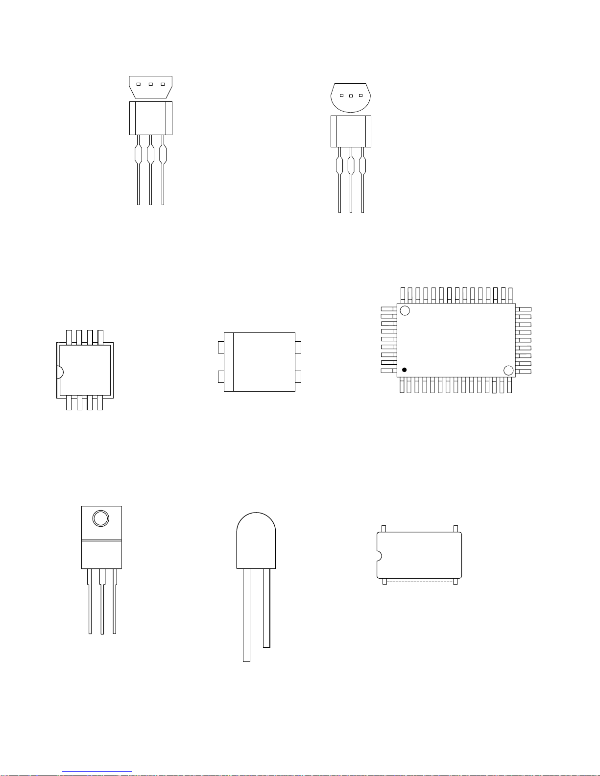
LEAD IDENTIFICATIONS
BR24C02F-W
AT24C02N-10SC
M24C02-MN6T
CAT24WC02JI
8
5
E C B
BN1F4M-T
BA1F4M-T
KTA1266(GR)
KTC3199(Y,GR,BL)
2SC2785(J.H.F.K)
KRA103M
KRC103M
KRA104M
BN1L4M-T
KTA1281(Y)
LTV-817(B.C)-F
EL817(A,B,C)
A
2SC1815-Y(TPE2)
2SC1815-GR(TPE2)
2SC2120-Y(TPE2)
KTC3203(Y)
2SC1815-BL(TPE2)
2SA1020(Y)
2SB892(S)
2SA1015-GR(TPE2)
E C B
LA71750AM-MTB
QSZAB0RMB111
80
81
C
51
50
1
FS1KM-18A
FS1KM-14A
G D S
4
K
PT204-6B-12
MID-32A22
C
E
E
100
1
TC4052BF(EL)
BU4052BCF-E2
CD4052BCSJX
16
1
9
8
31
30
Note:
A: Anode
K: Cathode
E: Emitter
C: Collector
B: Base
R: Reference
S: Source
G: Gate
D: Drain
1-12-1 HC341LE
Page 36

DECK MECHANISM
SECTION
VIDEO CASSETTE RECORDER
VCR425
Sec. 2: Deck Mechanism Section
I
Standard Maintenance
I
Alignment for Mechanism
I
Disassembly/Assembly of Mechanism
I
Alignment Procedures of Mechanism
TABLE OF CONTENTS
Standard Maintenance. . . . . . . . . . . . . . . . . . . . . . . . . . . . . . . . . . . . . . . . . . . . . . . . . . . . . . . . . . . . . . . . . . . 2-1-1
Service Fixtures and Tools . . . . . . . . . . . . . . . . . . . . . . . . . . . . . . . . . . . . . . . . . . . . . . . . . . . . . . . . . . . . . . .2-2-1
Mechanical Alignment Procedures . . . . . . . . . . . . . . . . . . . . . . . . . . . . . . . . . . . . . . . . . . . . . . . . . . . . . . . . . 2-3-1
Disassembly / Assembly Procedures of Deck Mechanism . . . . . . . . . . . . . . . . . . . . . . . . . . . . . . . . . . . . . . .2-4-1
Alignment Procedures of Mechanism . . . . . . . . . . . . . . . . . . . . . . . . . . . . . . . . . . . . . . . . . . . . . . . . . . . . . . .2-4-9
Page 37
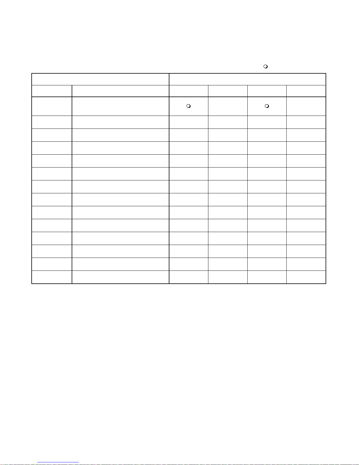
STANDARD MAINTENANCE
Service Schedule of Components
H: Hours : Check I : Change
Deck Periodic Service Schedule
Ref.No. Part Name 1,000 H 2,000 H 3,000 H 4,000 H
B2 Cylinder Assembly
B3
B8 Pulley Assembly
B27
B31
B573,B574 Reel S, Reel T
B37
B52
*B73 FE Head
B133
B410
B414 M Brake S Assembly II
B416
Loading Motor Assembly
Tension Lever Sub Assembly
AC Head Assembly
Capstan Motor
Cap Belt
Idler Assembly
Pinch Arm (A) Assembly
M Brake T Assembly
II
I
II
II
I
I
II
II
I
II
II
II
B525
Notes:
1.Clean all parts for the tape transp ort (Upper Drum with Video Head / Pi nch Roller / Audio Co ntrol Head / Full
Erase Head) using 90% lsopropyl Alcohol.
2.After cleaning the parts, do all DECK ADJUSTMENTS.
3.For the reference numbers listed above, refer to Deck Exploded Views.
* B73 ------ Recording Model only
LDG Belt
II
2-1-1 U25MEN
Page 38
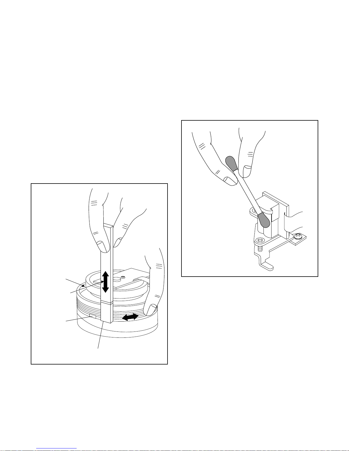
Cleaning
Cleaning of Video Head
Clean the head with a head cleanin g stick or chamois
cloth.
Procedure
1.Remove the top cabinet.
2.Put on a glove (thin type) to avoid touching the
upper and lower drum with your bare hand.
3.Put a few drops of 90% Isoprop yl alcohol on the
head cleaning stick or on the chamois cloth and,
by slightly pressi ng it a gai ns t th e he ad tip , tur n the
upper drum to the right and to the left.
Notes:
1.The video head surface is made of very hard
material, but since it i s very thin, avoid clea ning it
vertically.
2.Wait for the c leaned part to dry thorou ghly before
operating the unit.
3.Do not reuse a stained head cleaning stick or a
stained chamois cloth.
Cleaning of Audio Control Head
Clean the head with a cotton swab.
Procedure
1.Remove the top cabinet.
2.Dip the cotton swab in 90% is opropyl alcohol and
clean the audio control head. Be careful not to
damage the upper drum and other tape running
parts.
Notes:
1.Avoid cleaning the audio control head vertically.
2.Wait for the cleaned part to dry thoro ughly before
operating the unit or damage may occur.
A/C Head
Upper
Cylinder
Do Not !
Video Head
Cleaning Stick
2-1-2 U25MEN
Page 39
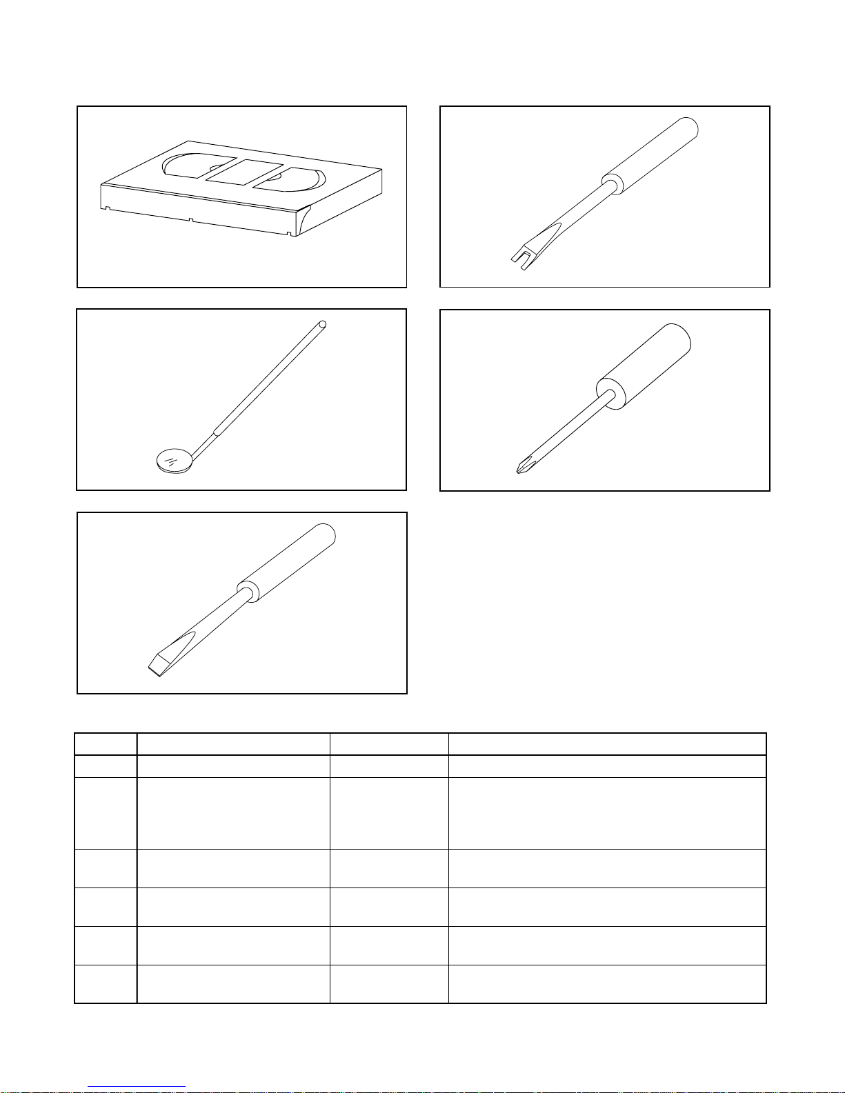
SERVICE FIXTURE AND TOOLS
J-1-1, J-1-2
J-3
J-2
J-4
J-5
Ref. No. Name Part No. Adjustment
J-1-1 Alignment Tape FL6A Head Adjustment of Audio Control Head
J-1-2 Alignment Tape FL6N8
J-2 Guide Roller Adj.Screwdr i ve r Available
J-3 Mirror Available
J-4 Azimuth Adj.Screwdriver + Available
J-5 X Value Adj.Screwdriver - Available
(1 speed only)
FL6NS8
(2 speed only)
Locally
Locally
Locally
Locally
2-2-1 U25PFIX
Azimuth and X Value Adjustment of Audio Control
Head / Adjustment of Envelope Waveform
Guide Roller
Tape Transportation Check
A/C Head Height
X Value
Page 40
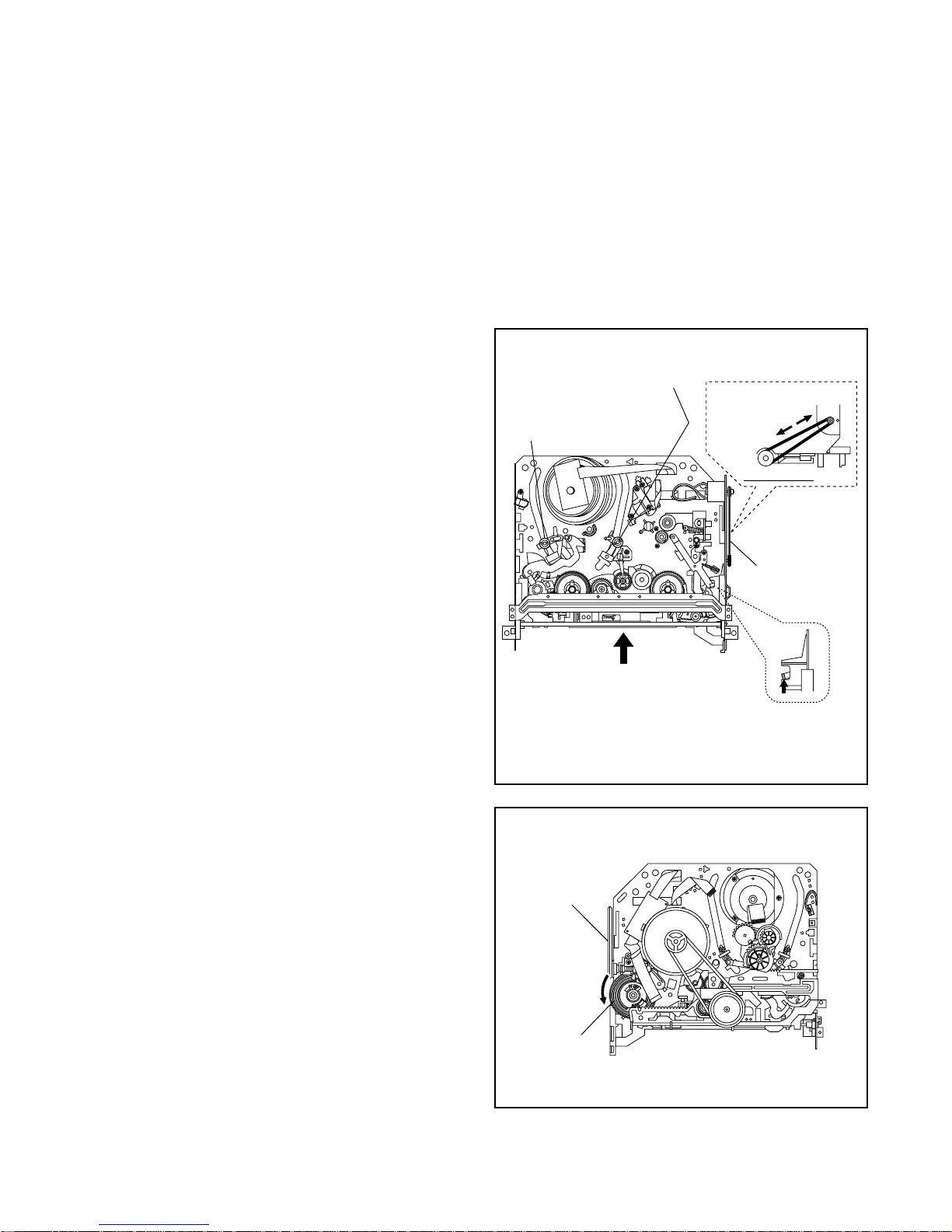
MECHANICAL ALIGNMENT PROCEDURES
Explanation of alignme nt for the tape to correctly run
starts on the next page. Refer to the information below
on this page if a tape gets stuck, for example, in the
mechanism due to some electrical trouble of the unit.
Service Information
Method for Manual Tape Loading/Unloading
A.
To load a cassette tape manually:
1. Disconnect the AC plug.
2. Remove the Top Case and Front Assembly.
3. Insert a cassette tape. Though the tape will not be
automatically loaded, make sure that the cassette
tape is all the way in at the inlet of the Cassette
Holder. To confirm this, ligh tly push the cassette
tape further in and se e if the ta pe comes bac k out,
by a spring motion, just as much as you have
pushed in.
4. Turn the LDG Belt in the appropriate direction
shown in Fig. M1 f or a minute or two to complete
this task.
To unload a cassette tape manually:
1. Disconnect the AC plug.
2. Remove the Top Case and Front Assembly.
3. Make sure that the M oving guide prepar ations are
in the Eject Position.
4. Turn the LDG Belt in the appropriate direction
shown in Fig. M1 unti l the Moving guide preparations come to the Eject Position. Stop turning
when the preparations b egin clicki ng or can not be
moved further. However, the tape will be left
wound around the cylinder.
5. Turn the LDG Belt in the approp riate directi on con tinuously, and the cassette tape will be ejected.
Allow a minute or two to complete this task.
Method to place t he Cassette Holder in the tape-
B.
loaded position without a cassette tape
1. Disconnect the AC Plug.
2. Remove the Top Case and Front Assembly.
3. Turn the LDG Belt in the appropriate direction
shown in Fig. M1. Rel ea se the lo ck in g ta bs shown
in Fig. M1 and contin ue turning the LDG Belt un til
the Cassette Holder comes to the tape-loaded
position. Allow a minute or two to complete this
task.
Top View
Moving guide T preparation
(Eject Position)
Moving guide S preparation
(Eject Position)
Push the tape
to load it.
Push the locking tab gently to unlock
when loading without a cassette.
UNLOAD
/EJECT
LOAD
Side View
LDG Belt
Fig. M1
Bottom View
LDG Belt (B)
UNLOAD
/EJECT
Cam Gear
Fig. M2
2-3-1 U25PALMA
Page 41
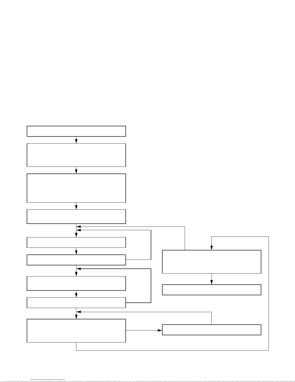
1.Tape Interchangeability Alignment
Note:
To do these alignment procedures, make sure that the
Tracking Control Circuit is set to the center position
every time a tape is loaded or unloaded. (Refer to
page 2-3-4, procedure 1-C, step 2.)
Equipment required:
Dual Trace Oscilloscope
VHS Alignment Tape (FL6N8)
Guide Roller Adj. Screwdriver
X-Value Adj. Screwdriver
Note: Before starting this Mechanical Alignment, do all
Electrical Adjustment procedures.
Flowchart of Alignment for tape traveling
Loading (Use a blank tape.)
Adjust the height of the Guide Rollers
(Supply side and take-up side).
(Use a blank tape.) (pg. 2-3-3)
1-A
Check to see that the tape is not creasing
and that there is no slack on the supply
and take-up side Guide Rollers.
(Use a blank tape.)
1-A
Adjust the X Value for maximum envelope.
(pg. 2-3-3) (Use Alignment Tape.)
Adjust the envelope. (pg. 2-3-4)
Check the envelope.
1-B
1-C
1-C
OK
Adjust the Audio Section.
(Azimuth Alignment) (pg. 2-3-4)
Check the audio output.
1-D
1-D
OK
Not good
Not good
Not good
Do the final tape-traveling test to see that
the tape runs normally in play mode without creasing or slacking.
OK
Completion
1-A
Check the following:
1. X Value (pg. 2-3-3)
2. Envelope (pg. 2-3-4)
OK
1-B, 1-C
Not good
2-3-2 U25PALMA
Adjust the X value and envelope.
1-B, 1-C
Page 42
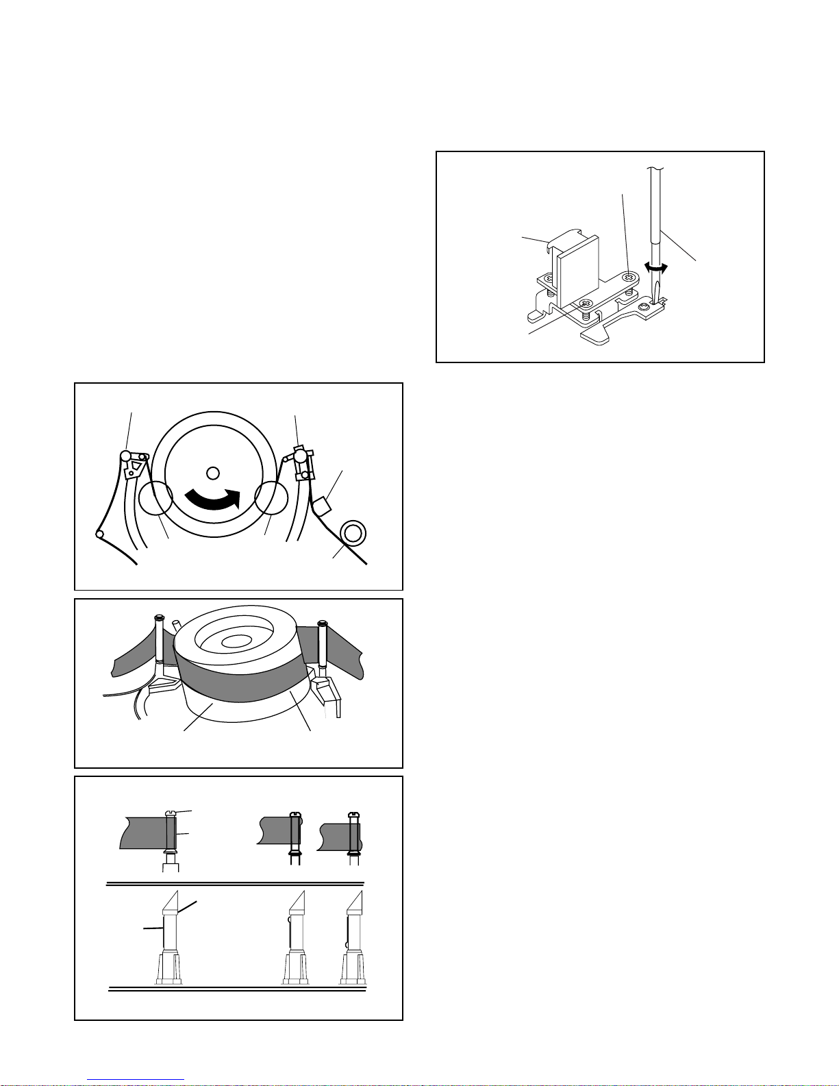
1-A. Preliminary/Final Checking and
Alignment of Tape Path
Purpose:
To make sure that the tape path is well stabilized.
Symptom of Misalignment:
If the tape path is unstable, the tape will be damaged.
Do not use an Alignment Tape for this proce-
Note:
dure. If the unit is not correctly alig ned, the tape ma y
be damaged.
1. Playback a blank cassette tape and check to see
that the tape runs without creasing at Guide Rollers
[2] and [3], and at points A and B on the lead s urface. (Refer to Fig M3 and M4.)
2. If creasing is apparent, align the height of the guide
rollers by turning the to p of Guide Rollers [2] and
[3] with a Guide Roller Adj. Screwdriver. (Refer to
Fig. M3 and M5.)
Guide Roller [2]
A
Take-up Guide Post [4]
Lead Surface of Cylinder
Correct
Guide Roller
Tape
Guide Roller [3]
B
Tape
Incorrect
AC Head
Fig. M3
Fig. M4
3. Check to see that th e tape run s witho ut cr ea si ng at
Take-up Guide Post [4] or without snaking between
Guide Roller [3] and AC Head. (Fig. M3 and M5)
4. If creasing or snaking is apparent, adjust the Tilt
Adj. Screw of the AC Head. (Fig. M6)
Azimuth Adj. Screw
AC Head
X-Value Adj.
Screwdriver
Tilt Adj. Screw
Fig. M6
1-B. X Value Alignment
Purpose:
To align the Horizon tal Position of the Audio/Contr ol/
Erase Head.
Symptom of Misalignment:
If the Horizontal Position of the Audio/Control/Erase
Head is not proper ly a ligned , m ax imu m e nv el ope ca nnot be obtained at the Neutra l positio n of the Track ing
Control Circuit.
1. Connect the oscilloscope to TP301 (C-PB) and
TP501 (CTL) on the Main CBA. Use TP502 (RFSW) as a trigger.
2. Playback the Gray Scale of the Alignment Tape
(FL6N8) and confirm that the PB FM signal is
present.
3. Set the Tracking C ontrol Circuit to the center p osition by pres si ng CH U P but to n the n “ PLA Y ” bu tt on
on the unit. (Refer to note on bottom of page
2-3-4.)
4. Use the X-Value Adj. Screwdriver so that the PB
FM signal at TP301 (C-PB) is maximum. (Fig. M6)
5. Press CH UP button on the unit until the CTL waveform has shifted by approx. +2msec. Make sure
that the envelope is simply attenuated (shrinks in
height) during this process so that you will know
the envelope has been at its peak.
Take-up Guide
Post
Tape
Fig. M5
2-3-3 U25PALMA
Page 43
6. Press CH DOWN butto n on the unit until the CTL
waveform has s hifted from it s original position ( not
the position achie ved in step 5, b ut the position of
CTL waveform in step 4) by approximately -2msec.
Make sure that th e envelope is simply attenuated
(shrinks in height) once CTL waveform passes its
original position and is fur ther bro ught in the minu s
direction.
7. Set the Tracking Contr ol Circuit to th e center posi tion by pressing CH UP button and the n “ PLAY ”
button.
1-C. Checking/Adjustment of Envelope
Waveform
Purpose:
To achieve a satisfactory picture and precise tracking.
Symptom of Misalignment:
If the envelope out put is poor , noise will appear in the
picture. The tracki ng will then lose precision and the
playback picture w ill be distorted by any sligh t variation of the Tracking Control Circuit.
1. Connect the oscillos cope to TP301 (C-PB) on the
Main CBA. Use TP502 (RF-SW) as a trigger.
2. Playback the Gray Scale on the Alignment Tape
(FL6N8). Set the Tracking Control Circuit to the
center position by pressing CH UP b utton and then
“ PLAY ” button on the unit. Ad just the height of
Guide Rollers [2] and [3] (Fig. M3, Page 2-3-3)
watching the oscill oscope di splay so that the enve lope becomes as flat as possible. To do this adjustment, turn the top of the Guide Roller with the
Guide Roller Adj. Screwdriver.
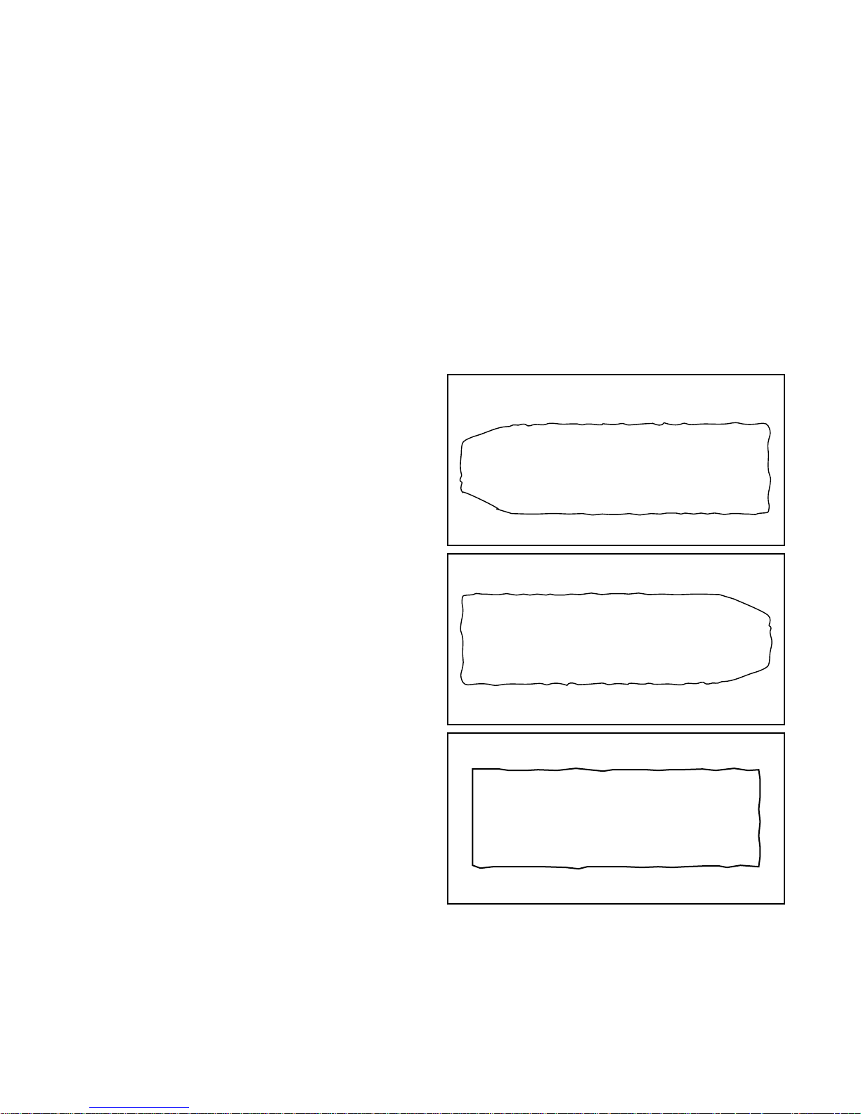
3. If the envelope is as shown in Fig. M7, adjust the
height of Guide Ro ll er [2] (Re fer to Fig. M3) s o that
the waveform looks like the one shown in Fig. M9.
4. If the envelope is as shown in Fig. M8, adjust the
height of Guide Ro ll er [3] (Re fer to Fig. M3) s o that
the waveform looks like the one shown in Fig. M9.
5. When Guide Roller s [2] and [3] (Refer to Fig.M3)
are aligned properly, there is no envelope drop
either at the beginning or end of track as shown in
Fig. M9.
Note: Upon completion of the adjustment of Guide
Rollers [2] and [3] (Refer to Fig. M3), check the X
Value by pushin g the CH UP or DOWN b uttons alternately, to check the symm etry of the env elope. Chec k
the number of pushe s to ensure cente r position. The
number of pushes CH UP button to ac hieve 1/2 level
of envelope should m atch the number of pushes CH
DOWN button from center. If required, redo the “X
Value Alignment.”
1-D. Azimuth Alignment of Audio/Control/
Erase Head
Purpose:
To correct the Azimuth alignment so that the Audio/
Control/Erase Head meets tape tracks properly.
Symptom of Misalignment:
If the position of the Audio/Control/Erase Head is not
properly aligned, the Audio S/N Ratio or Frequency
Response will be poor.
1. Connect the oscilloscope to the audio output jack
on the rear side of the deck.
2. Playback the alig nment tape (FL6N8) and confi rm
that the audio signal output level is 8kHz.
3. Adjust Azimuth Adj. Screw so that the output level
on the AC Voltmeter or the waveform on the oscilloscope is at maximum. (Fig . M6)
Dropping envelope level at the beginning of track.
Fig. M7
Dropping envelope level at the end of track.
Fig. M8
Envelope is adjusted properly. (No envelope drop)
Fig. M9
2-3-4 U25PALMA
Page 44
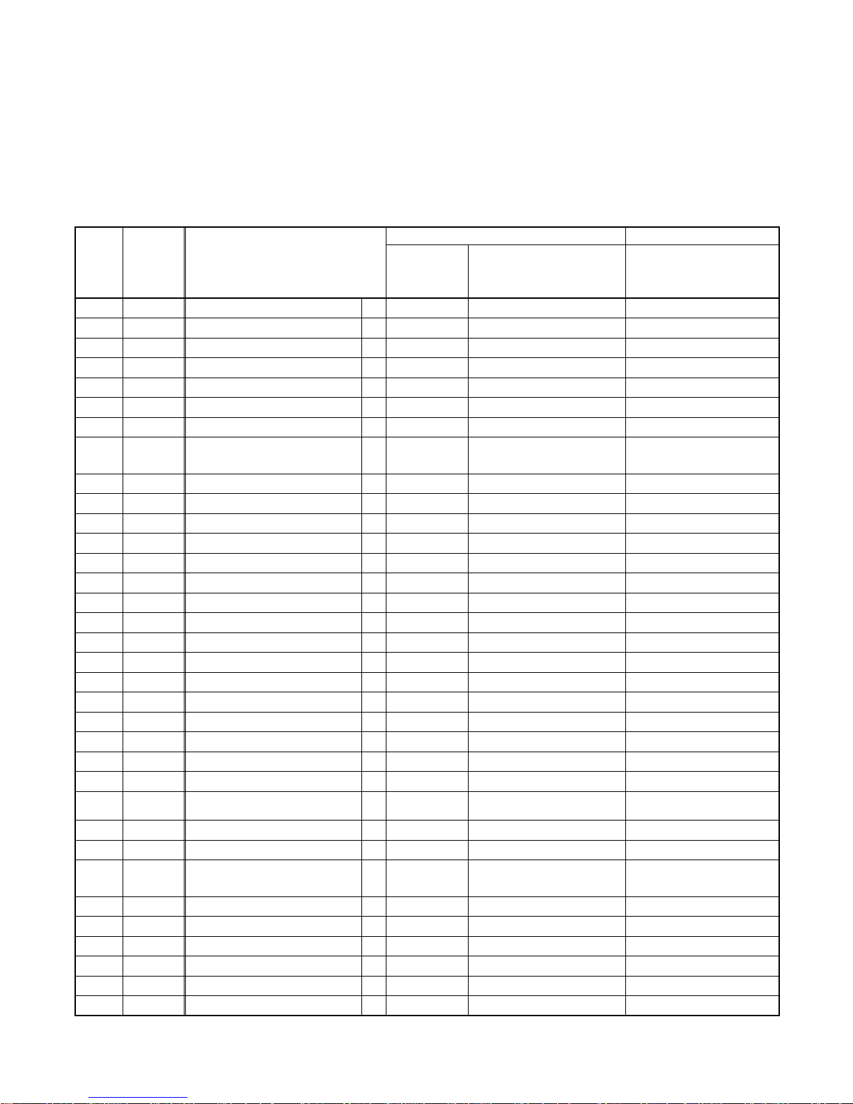
DISASSEMBLY/ASSEMBLY PROCEDURES
OF DECK MECHANISM
Before following the procedures described below, be sure to remove the deck assembly from the cabinet. (Refer to
CABINET DISASSEMBLY INSTRUCTIONS on page 1-5-1.)
All the following proc edures, including those for adjustment and replacement of par ts, should be done in Eject
mode; see the positions of [45] and [46] in Fig.DM1 on page 2-4-3. When reassembling, follow the steps in reverse
order.
STEP
/LOC.
START-
ING
No.
[1] [1]
[2] [1] Cassette Holder Assembly T DM4
[3] [2]
[4] [2]
[5] [4]
[6] [2] C Plate T DM5
[7] [7]
[8] [8]
[9] [9]
[10] [2] Tape Guide Assembly T DM1,D M8 *(P-2)
[11] [10]
[12] [11]
[13] [12]
[14] [14] FE Head T DM1,DM9 (S-9)
[15] [15]
[16] [2]
[17] [16]
[18] [16] C Drive Lever R T DM10
[19] [7],[10] Capstan Motor B DM2,DM11 3(S-12), Cap Belt
[20] [20]
[21] [20]
[22] [22] Cam Holder F B DM2,DM13 (C-2)
[23] [22] Cam Gear (B) B DM2,DM13 (C-3),*(P-4)
[24] [24]
[25]
[26] [22]
[27] [26]
[28] [22],[25]
[29] [20] TR Gear C B DM2,DM14 (C-6)
[30] [29]
[31] [30]
[32] [31]
[33] [21],[25] Idler Assembly(HI) B DM1,DM15 *(L-5)
[34] [25]
No.
[20],[23],
[24]
Guide Holder A T DM3 2(S-1)
Slider L T DM5 (S-2)
Slider R T DM5 (S-3)
Lock Lever T DM5 (S-4),*(P-1)
Cylinder Assembly T DM1,DM6 Desolder, 3(S-5)
Loading Motor Assembly T DM1,DM7
AC Head Assembly T DM1,DM7 (S-7)
Door Opener B T DM1,DM8 *(L-1),*(L-2)
Pinch Arm (B) T DM1,DM8 *(P-3)
Pinch Arm (A) Assembly T DM1,DM8
Prism T DM1,DM9 (S-10)
Slider Shaft T DM10 (S-11),*(L-3)
C Drive Lever L T DM10
Clutch Assembly(HI) B DM2,DM12 (C-1)
Center Gear B DM12
Mode Gear B DM2,DM14 (C-4)
Mode Lever(HI) B DM2,DM14 (C-5), *(L-4)
Worm Holder B DM2,DM14 (S-15)
Pulley Assembly B DM2,DM14
Cam Gear (A) B DM2,DM14
TR Gear Spring B DM14
TR Gear A/B B DM1,DM14
FF Arm(HI) B DM1,DM14
BT Arm B DM2,DM15 *(P-5)
PART
Fig. No.
REMOVAL INSTALLATION
REMOVE/*UNHOOK/
UNLOCK/RELEASE/
UNPLUG/DESOLDER
Desolder, LDG Belt,
2(S-6)
ADJUSTMENT
CONDITION
(+)Refer to Alignment
Sec.Pg.2-4-10
2-4-1 U25PALDA
Page 45
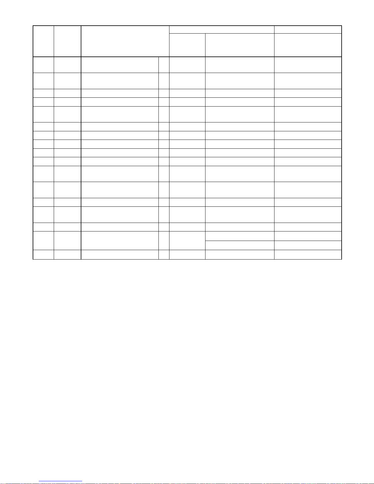
STEP
/LOC.
START-
ING
No.
No.
[35] [25]
[36] [35]
[37] [2],[25]
PART
Fig. No.
REMOVE/*UNHOOK/
UNLOCK/RELEASE/
UNPLUG/DESOLDER
Loading Arm S(B)
Assembly
Loading Arm T(B)
Assembly
B DM2,DM15
B DM2,DM15
M Brake T(HI) Assembly T DM1,DM16 *(P-6)
(+)Refer to Alignment
Sec.Pg.2-4-9
(+)Refer to Alignment
Sec.Pg.2-4-9
[38] [2],[25] M Brake S(HI) Assembly T DM1,DM16 *(P-7)
REMOVAL INSTALLATION
[39] [38]
[40] [39]
[41] [2]
Tension Lever Sub
Assembly
T DM1,DM16
T Lever Holder T DM1,DM16 * (L-6 )
M Gear(HYT) T DM1,DM16 (C-7)
[42] [2],[15] Sensor Gear T DM1,DM16 (C-8)
[43] [37],[41] Reel T T DM1,DM16
[44] [39]
[45] [35],[38]
[46] [36]
Reel S T DM1,DM16
Moving Guide S
Preparation
Moving Guide T
Preparation
T DM1,DM17
T DM1,DM17
[47] [19] TG Post Assembly T DM1,DM17 *(L-7)
[48] [18],[28]
[49] [48]
Rack Assembly R DM18
F Door Opener R DM18
[50] [50] Cleaner Lever Assembly T DM1,DM6
*(L-8) Type B
(+)Refer to Alignment
Sec.Pg.2-4-10
Type A
[51] [50] CL Post T DM6 *(L-9) Type A
↓
(1)
↓
(2)
↓
(3)
↓
(4)
↓
(5)
↓
(6)
ADJUSTMENT
CONDITION
↓
(7)
(1): Follow steps in sequence. When reassembling, follow the steps in reverse order.
These numbers are also used as identification (location) No. of parts in the figures.
(2): Indicates the part to start disassembling with in order to disassemble the part in column (1).
(3): Nam e of the part
(4): Location of the part: T=Top B=Bottom R=Right L=Left
(5): Figure Number
(6): Identification of parts to be removed, unhooked, unlocked, released, unplugged, unclamped, or desoldered.
P=Spring, W=Washer, C=Cut Washer, S=Screw, *=Unhook, Unlock, Release, Unplug, or Desolder
e.g., 2(L-2) = two Locking Tabs (L-2).
(7): Adjustment Information for Installation
(+):Refer to Deck Exploded Views for lubrication.
.
2-4-2 U25PALDA
Page 46
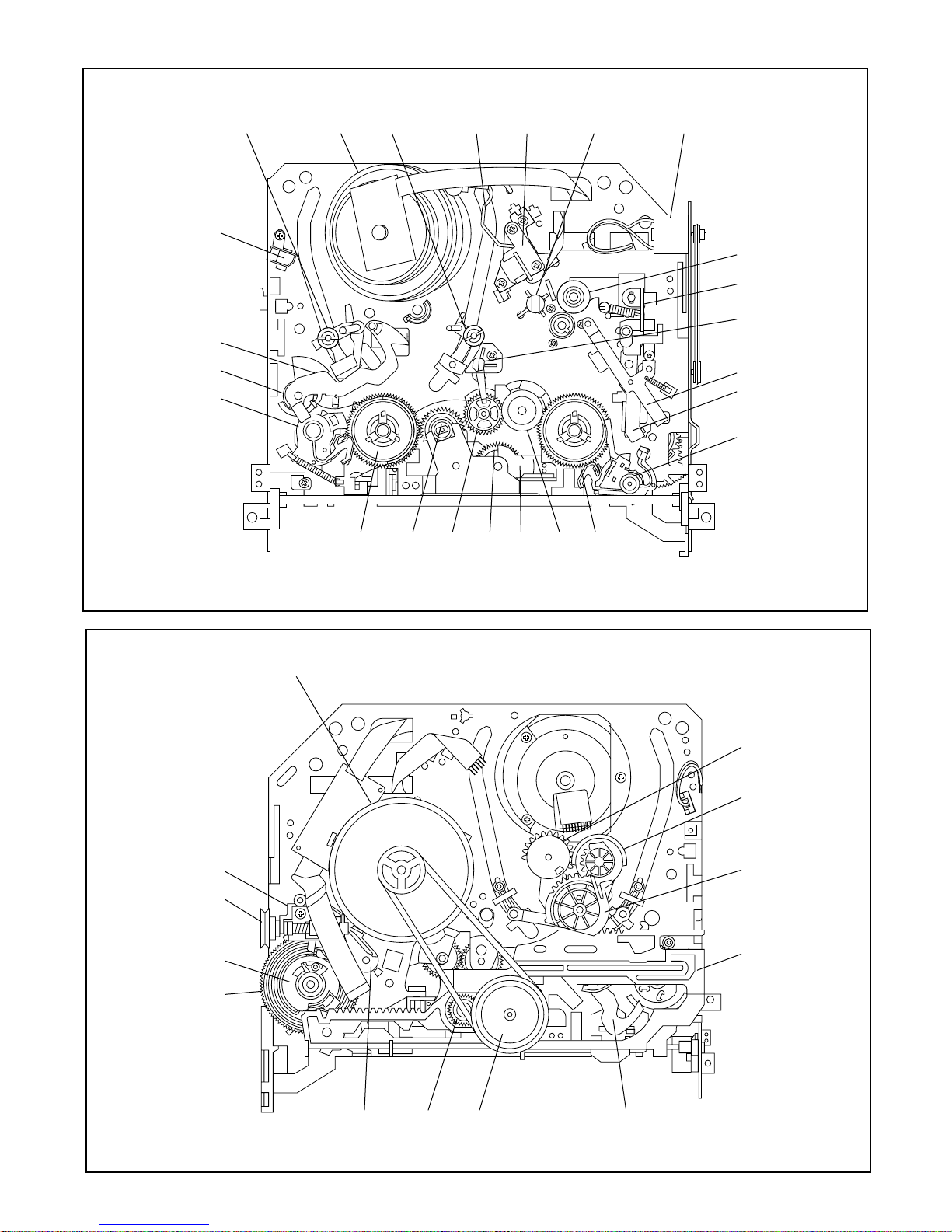
T op View
[14]
[39]
[7] [50] [8]
[46][45] [47][9]
[13]
[11]
[15]
[40]
[38]
Bottom View
[10]
[12]
[37]
[33][44] [42] [31] [32] [41] [43]
Fig. DM1
[19]
[36]
[35]
[26]
[27]
[23]
[28]
[24]
[25]
[34][20][29][22]
Fig. DM2
2-4-3 U25PALDA
Page 47
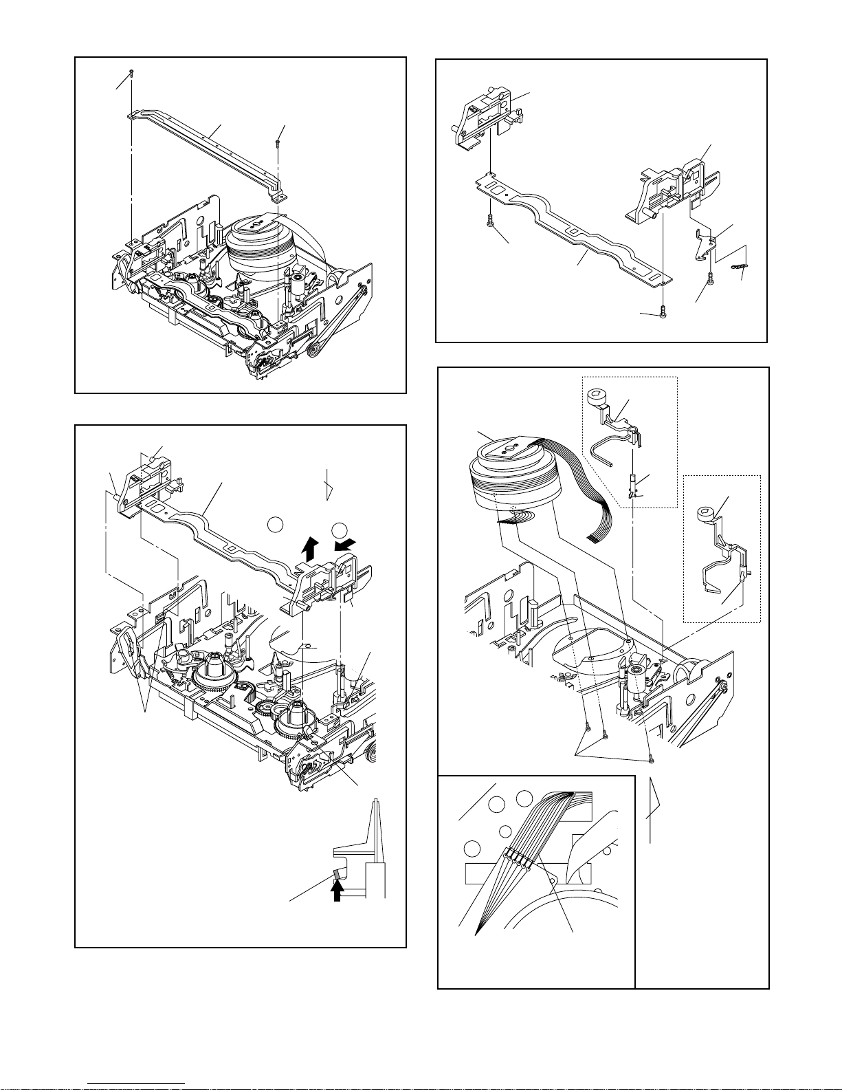
(S-1)
[1]
(S-1)
(S-2)
[3]
[6]
(S-3)
[4]
[5]
(P-1)
(S-4)
Fig. DM5
Pin C
Slots B
Pin D
[2]
Pin A
2
Pull up
Fig. DM3
A
1
Slide
Pin B
Slot A
[7]
Type A
(S-5)
[50]
[51]
(L-9)
Type B
[50]
(L-8)
First, while pushing the locking tab as
shown in the right, slide and pull up the right
side on [2] to release Pin A and Pin B from
the slots A.
Then, remove Pin C and Pin D on [2] from
the slots B as shown.
Locking tab
Slot A
View for A
Fig. DM4
A
Desolder
from bottom
View for A
Lead with
Blue Stripe
Fig. DM6
2-4-4 U25PALDA
Page 48
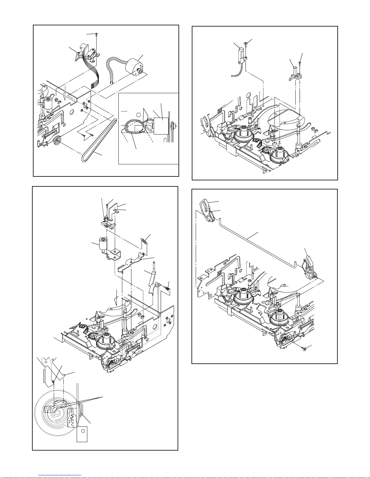
[9]
A
(S-7)
(S-6)
(L-2)
LDG
Belt
Adj. Screw
[8]
Desolder
from bottom
Lead with White Stripe
View for A
[8]
Fig. DM7
[11]
(L-1)
[17]
(L-3)
[14]
(S-9)
(S-10)
[15]
Fig. DM9
After removing the Screw (S-11),
while pressing the Locking Tab
(L-3), remove [16].
Pin of [12]
Pin of [10]
[13]
[10]
A
Grooves of [28]
(P-3)
[12]
[16]
[18]
(P-2)
(S-11)
Fig. DM10
When reassembling [10] and
[12], confirm that pin of [10]
and pin of [12] are in the
[28]
grooves of [28] as shown.
View for A
Fig. DM8
2-4-5 U25PALDA
Page 49
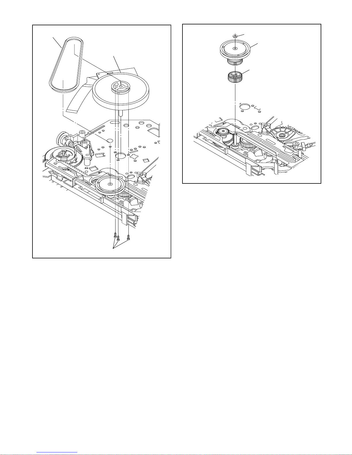
Cap Belt
(C-1)
[20]
[19]
[21]
Fig. DM12
(S-12)
Fig. DM11
2-4-6 U25PALDA
Page 50
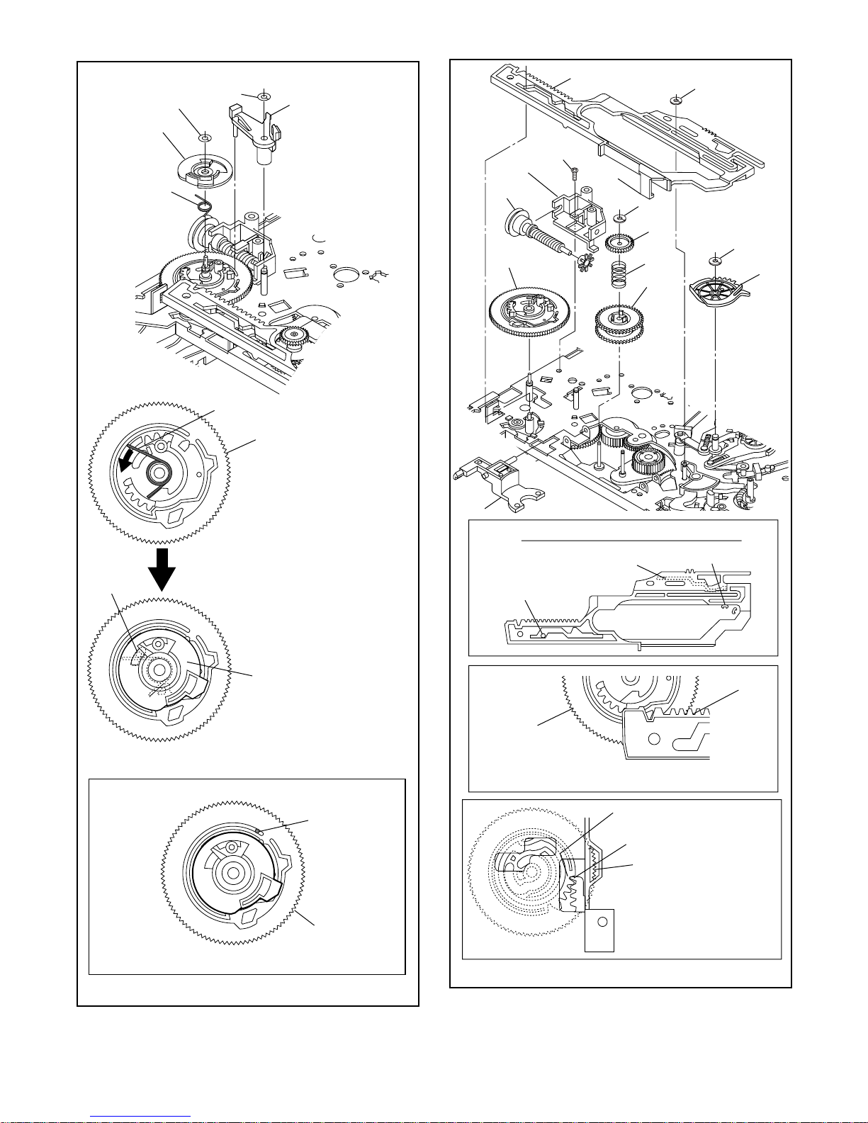
[23]
(P-4)
(C-3)
(C-2)
(P-4)
[28]
[22]
[27]
[28]
[26]
(S-15)
[25]
(L-4)
(C-6)
[29]
[30]
[31]
(C-5)
(C-4)
[24]
Pin on
bottom
of [23]
T op Vie w
When installing [23], install
the spring (P-4) to [28] as
shown in the left figure, and
then install [23] while
pressing the spring (P-4) to
the direction of the arrow in
the left figure and confirming
that the position of the
spring (P-4) is placed as
shown in the left figure.
[23]
Position of pin on [22]
Pin on [22]
[28]
Fig. DM13
[32]
Pin of [37]
Bottom View
T op Vie w
Position of Mode Lever when installed
Pin of [34]
[28]
Align [25] and [28] as shown.
First groove on [28]
First tooth on [48]
[28]
When reassembling [28],
meet the first groove on
[28] to the first tooth on
[48] as shown.
Pin of [38]
[25]
Fig. DM14
2-4-7 U25PALDA
Page 51
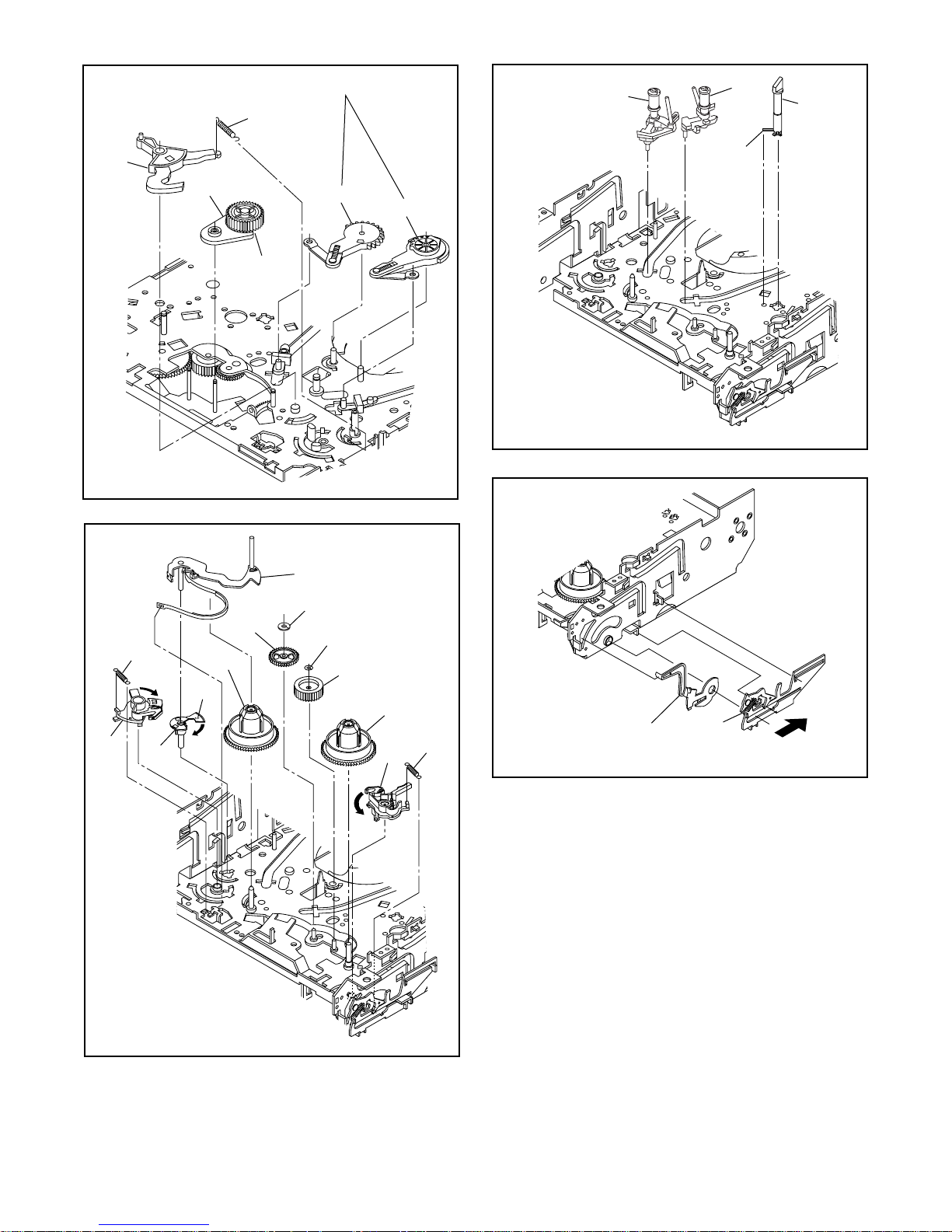
Refer to the Alignment Section, Page 2-4-9.
(P-5)
[45]
[46]
[47]
[34]
[38]
(P-7)
turn
[40]
[33]
(L-6)
turn
[44]
[42]
(L-5)
[39]
(C-8)
[36]
(C-7)
[41]
[35]
Fig. DM15
[43]
(P-6)
[37]
[49]
[48]
(L-7)
Fig. DM17
Slide
Fig. DM18
turn
Fig. DM16
2-4-8 U25PALDA
Page 52
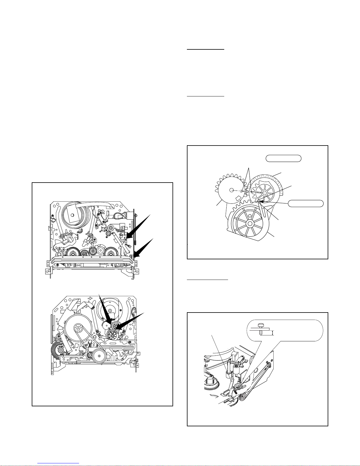
ALIGNMENT PROCEDURES OF MECHANISM
The following procedures describe how to align the
individual gears and levers that make up the tape
loading/unloading mechanism. Since information
about the state of the mechanism is provided to the
System Control Circuit on ly through the Mode Switch,
it is essential that the correct relationship between
individual gears and levers be maintained.
All alignments are to be performed with the mechanism in Eject mode, in the sequenc e given. Each
procedure assumes th at all pr evious pro cedures hav e
been completed.
IMPORTANT:
If any one of these alignments is not performed
properly, even if off by only one tooth, the unit will
unload or stop and it may result in damage to the
mechanical or electrical parts.
Alignment points in Eject Position
T op View
Alignment [a]
Alignment 3
Alignment 1
Loading Arm, S and T Assembly
Install Loading Arm S and T Assembly so that their
triangle marks point to each other as shown in Fig.
AL2.
Alignment 2
Mode Gear
Keeping the two triangles pointing at each other ,
install the Loading Arm T Assembly so that the last
tooth of the gear meets the most inside teeth of the
Mode Gear. See Fig. AL2.
Alignment 1
Triangle Marks
Loading Arm
T Assembly
Loading Arm
S Assembly
Last Tooth
Alignment 2
Most inside teeth
of Mode Gear
Mode Gear
Bottom View
Alignment [a] can be done independently of any
other alignment.
Alignment 1
Alignment 2
Fig. AL1
Fig. AL2
Alignment [a]
Tape Guide Assembly
Measurement of the screw must be as spe ci fied in
Fig. AL3.
Tape Guide
Assembly
Screw
3.25 – 0.1 mm
0.128 – 0.004 inch
This alignment can be
done independently of
any other alignment.
Fig. AL3
2-4-9 U25NAPM
Page 53
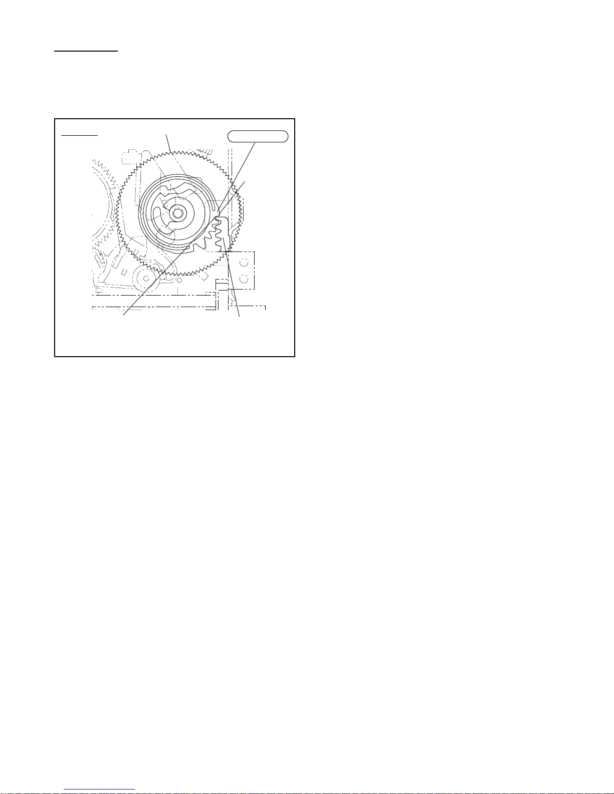
Alignment 3
Cam Gear (A), Rack Assembly
Install the Rack Asse mbl y so tha t the first tooth on
the gear of the Rack Assembly meets the first
groove on the Cam Gear (A) as shown in Fig. AL4.
Top View
First groove
on the Cam Gear (A)
Cam Gear (A)
Alignment 3
First tooth
Gear on Rack Assembly
Fig. AL4
2-4-10 U25NAPM
Page 54

EXPLODED VIEWS AND
PARTS LIST SECTION
VIDEO CASSETTE RECORDER
VCR425
Sec. 3: Exploded views
and Parts List Section
I
Exploded views
I
Parts List
TABLE OF CONTENTS
Exploded Views . . . . . . . . . . . . . . . . . . . . . . . . . . . . . . . . . . . . . . . . . . . . . . . . . . . . . . . . . . . . . . . . . . . . . . . .3-1-1
Mechanical Parts List. . . . . . . . . . . . . . . . . . . . . . . . . . . . . . . . . . . . . . . . . . . . . . . . . . . . . . . . . . . . . . . . . . . . 3-2-1
Electrical Parts List . . . . . . . . . . . . . . . . . . . . . . . . . . . . . . . . . . . . . . . . . . . . . . . . . . . . . . . . . . . . . . . . . . . . . 3-3-1
Deck Parts List. . . . . . . . . . . . . . . . . . . . . . . . . . . . . . . . . . . . . . . . . . . . . . . . . . . . . . . . . . . . . . . . . . . . . . . . . 3-4-1
Page 55
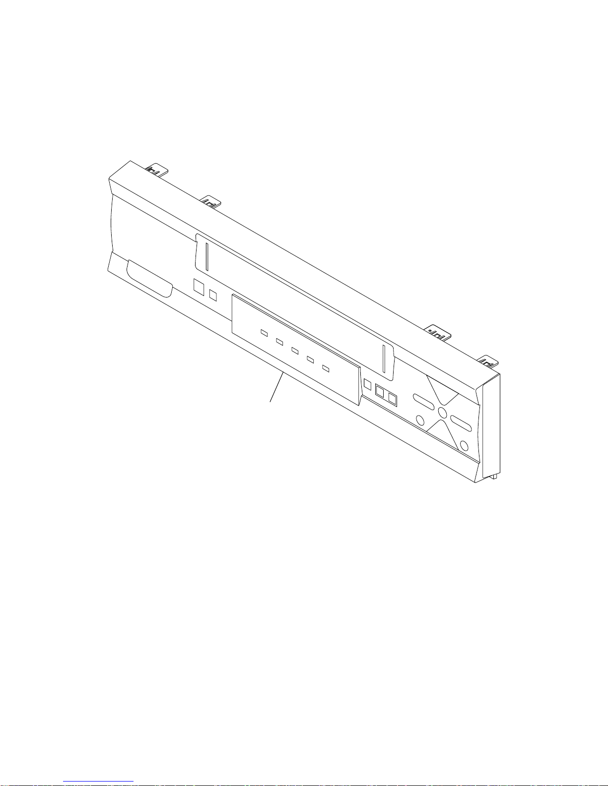
Front Panel
EXPLODED VIEWS
A1X
3-1-1 HC341FEX
Page 56
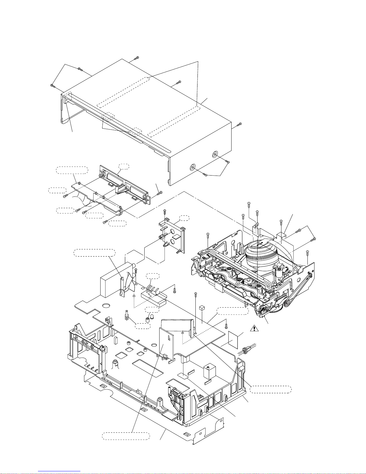
Cabinet
2L011
JACK CBA
2L022
2L022
2B9
2B9
2L022
2L022
A5
2L011
2L012
2L041
2L011
A4
2B18
A2
2L021
2L011
2L021
2L011
2L042
2L021
2L021
2B5
2L051
SENSOR CBA
2L041
2B46
2B7
2B8
2L031
2L041
2B14
MAIN CBA
2L099
A10
2B49
2L021
1B1
SENSOR CBA
A3
FUNCTION CBA
A7
3-1-2 HC2C0CEX
Page 57
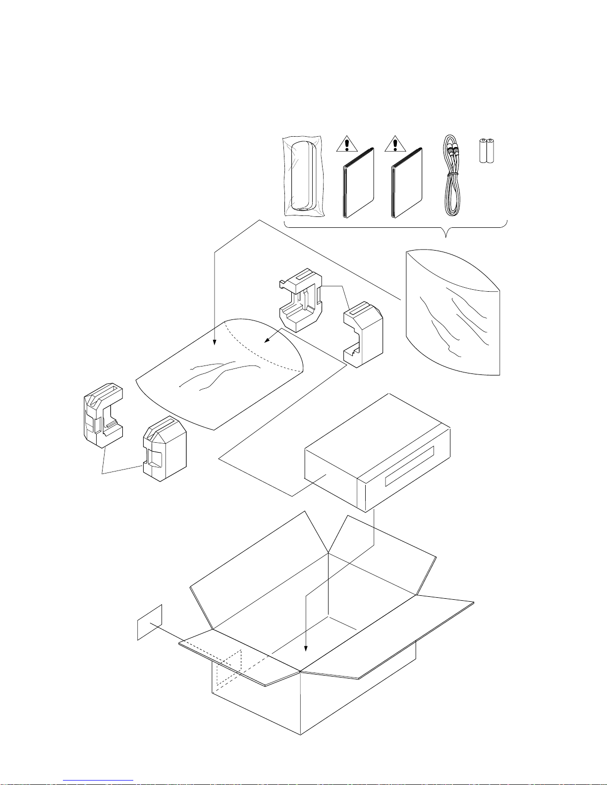
Packing
Some Ref. Numbers are not in sequence.
X1
X20B
S2
X20A
X3
X2
X4
S2
S3
Unit
A14
S1
3-1-3 HC341PEX
Page 58
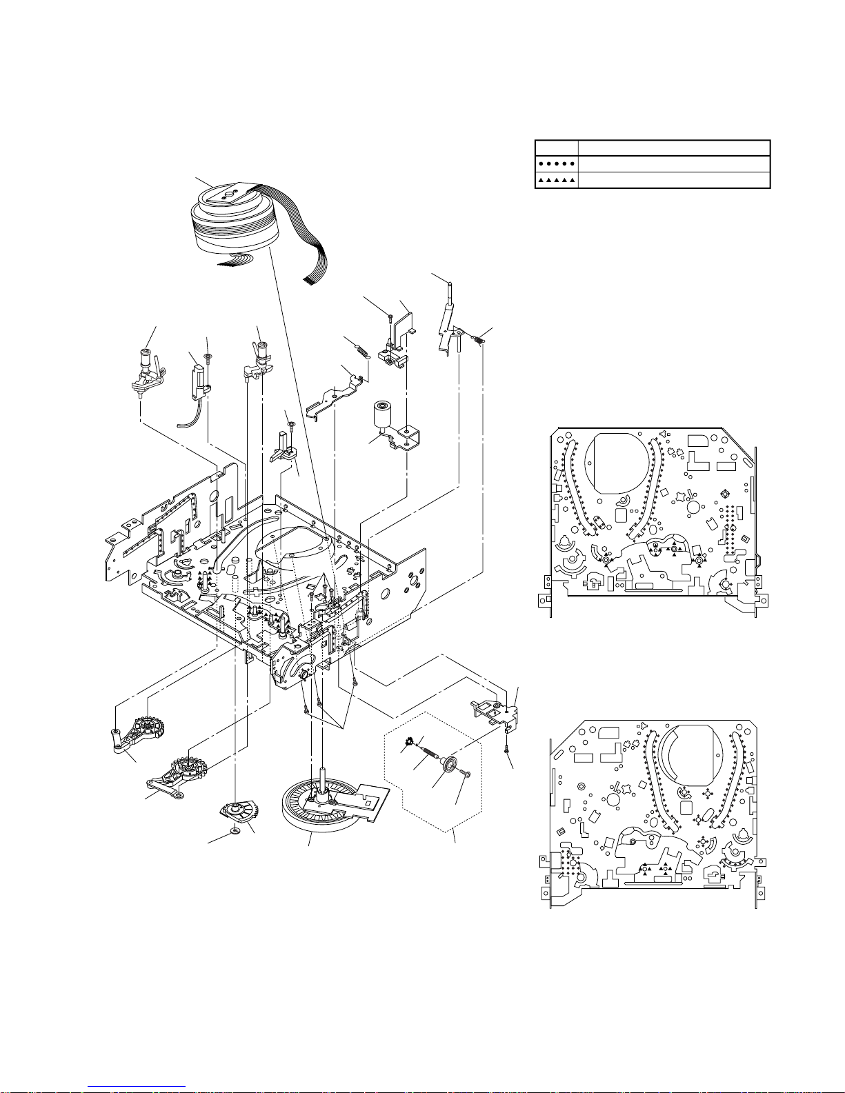
DECK EXPLODED VIEWS
Deck Mechanism View 1
B2
B35
Mark Description
Floil G-374G
SLIDUS OIL #150
(Blue grease)
B9
B73
L1191
B10
L1053
B74
L1051
L1467
B411
B567
B494
B553
B410
Chassis Assembly
Top View (Lubricating Point)
B501
B12
B11
B571
Some Ref. Numbers are not in sequence.
B492
B37
L1450
B560
B426
B121
B126
L1468
B8
L1466
Chassis Assembly
Bottom View (Lubricating Point)
3-1-4 U25PALDEX
Page 59
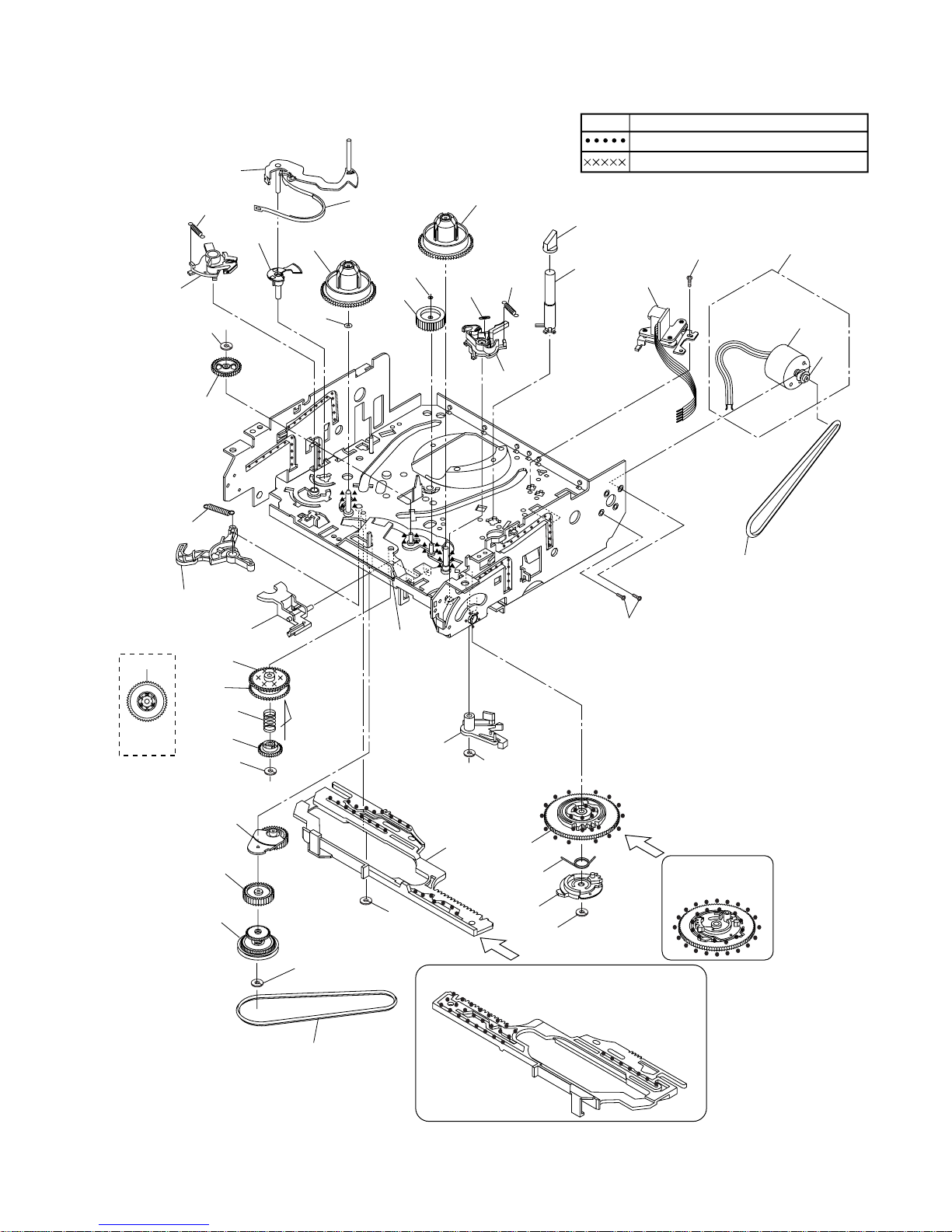
Deck Mechanism View 2
B27
B508
B499
B414
B572
B565
B573
B585
B487
B518
B564
B574
B521
B520
B416
Mark Description
Floil G-374G
SANKOUL FG84M
B148
L1406
B522
B31
(Blue grease)
(Yellow grease)
B3
B558
B557
B579
View
for A
B417
B568
B578
B579
B582
B580
B133
B581
B559
B551
B583
A
B516
B584
B507
B569
B505
B488
B491
B570
B502
B513
Bottom Side (Grease point)
B525
L1151
Bottom Side
(Grease point)
B52
Some Ref. Numbers are not in sequence.
3-1-5 U25PALDEX
Page 60
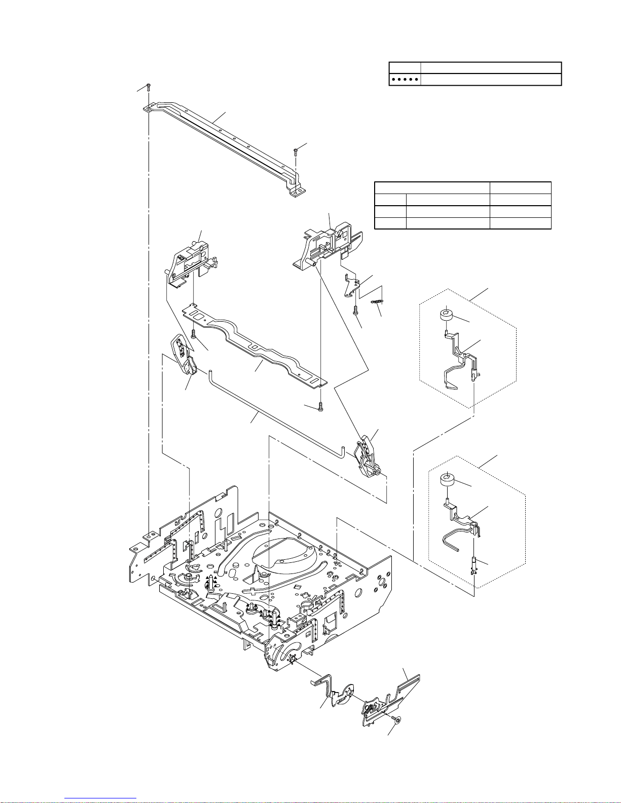
Deck Mechanism View 3
L1321
B355
L1341
B347
L1321
B354
Mark Description
Floil G-374G
Note: There are two different, but interchangeable
types of CLEANER LEVER(B359) in this model,
and have different combination with B361. Please
see Table 1 for details and combination. (Refer to
DECK PARTS LIST section.)
Table 1 (B359 and B361 Combination)
Type Part No. Part No.
A 0VM411114
B
B483
B425
L1461
0VM304413
0VM305090
B360
(Blue grease)
B361B359 CLEANER LEVER
Not used
B529
Type B
B359
B562
B482
B563
L1341
B300
B529
Type A
B360
B359
B361
B555
Some Ref. Numbers are not in sequence.
B303
B514
3-1-6 U25PALDEX
Page 61
MECHANICAL PARTS LIST
PRODUCT SAFETY NOTE: Products marked with a
have special characteristics important to safety.
!
Before replacing any of these components, rea d carefully the product safety notice in this service manual.
Don't degrade the safety of the product through
improper servicing.
NOTE:
Parts that are not assigned part numbers (---------) are
not available.
Ref. No. Description Part No.
A1X FRONT ASSEMBLY HC341ED 0VM203706
A2 CASE, TOP(ANTHRACITE) HC400EP 0VM101078
A3 CHASSIS(PAL-FTZ) HC460ED 0VM000159
A4 JACK BOARD(CONV) HC460ED
A5 JACK BOARD(2-21P) HC460ED
A7 PANEL, BOTTOM HC460ED 0VM203358
A10! LABEL, RATING HC341ED ---------A14 LABEL, SERIAL NO . H39H0JD(JPN) or 0VM409906
1B1 DECK ASSEMBLY CZD011/VM15C0 N15C0FL
2B5 SHEILD, CYLINDER HC460ED 0VM305182
2B7 SHIELD ASSEMBLY HC4 60ED
2B8 BUSH, LED(F) H3700UD (See Electrical Parts List)
2B9 CUSHION HC460ED 0VM413251
2B14 CUSHION(PCB) HC460ED 0VM413265
2B18 FIBER, TOP CASE HC460ED 0VM412906
2B46 ROHM HOLDER H7770JD (See Electrical Parts List)
2B49 CHASSIS FIBER HC460ED 0VM413311
2L011 SCREW, P-TIGHT 3X12 BIND HEAD+ GBCP3120
2L012 SCREW, P-TIGHT 3X12 BIND HEAD+ GBCP3120
2L021 SCREW, P-TIGHT M3X10 WASHER HEAD+ GCMP3100
2L022 SCREW, P-TIGHT M3X10 WASHER HEAD+
2L031 SCREW, B-TIGHT M3X8 BIND HEAD+ GBMB3080
2L041 P-TIGHT SCREW 3X8 BIND + GBMP3080
2L042 P-TIGHT SCREW 3X8 BIND + GBMP3080
2L051 SCREW, S-TIGHT M3X5 BIND HEAD+ GBMS3050
2L099 SCREW, P-TIGHT M3X8 BIND HEAD+ GBCP3080
S1 GIFT BOX CARTON HC341ED 0VM305614
S2 STYROFOAM HC460ED 0VM203356
S3 UNIT, BAG V4010PA 0VM406453B
X1 REMOTE CONTROL UNIT 364/CRC005 or N9472ED
X2 DRY BATTERY R6P/2S or XB0M451T0001
X3 RF CORD PAL 1.2M WPZ0122LG001
X4 ACCESSORY BAG K8092BA 0VM404632
X20A! OWNER'S MANUAL HC341ED 0VMN03179
X20B! OWNER'S MANUAL(SWEDISH) HC341ED 0VMN03181
(See Electrical Parts List)
(See Electrical Parts List)
LABEL, BAR CODE HC341ED 0VM413839
(See Electrical Parts List)
(See Electrical Parts List)
PACKING
ACCESSORIES
REMOTE CONTROL UNIT 364/CRC006 NA174ED
DRY BATTERY(SUNRISE) R6SSE/2S XB0M451MS002
20020613 3-2-1 HC341CA
Page 62
ELECTRICAL PARTS LIST
PRODUCT SAFETY NOTE: Products marked with a
have special characteristics important to safety.
!
Before replacing any of these components, rea d carefully the product safety notice in this service manual.
Don't degrade the safety of the product through
improper servicing.
NOTES:
1. Parts that a re not assigned part numbe rs (---------)
are not available.
2. Tolerance of Capacitors and Resistors are noted
with the following symbols.
C.....±0.25% D.....±0.5% F.....±1%
G.....±2% J......±5% K.....±10%
M.....±20% N.....±30% Z.....+80/-20%
MCV CBA
Ref. No. Description Part No.
MCV CBA
Consists of the following:
MAIN CBA (MCV-A)
FUNCTION CBA (MCV-B)
JACK CBA (MCV-E)
SENSOR CBA
MAIN CBA
Ref. No. Description Part No.
MAIN CBA(MCV-A)
Consists of the following:
CAPACITORS
C002! METALLIZED FI LM CAP. 0. 068µF/275V K or CT2E683HJE06
! METALLIZED FILM CAP. 0. 068µF/250V K or CT2E683DC011
! METALLIZED FILM CAP. 0. 068µF/250V M CT2E683MS037
C003! SAFETY CAP. 2200pF/250V or CCN2EMP0E222
! SAFETY CAP. 2200pF/250V CA2E222MR049
C004 ELECTROLYTIC CAP. 22µF/400V M(L•Z) or CA2H220NC010
ELECTROLYTIC CAP. 22µF/400V M CA2H220S6015
C005 CERAMIC CAP. B K 0.01µF/500V CCD2JKP0B103
C006 CERAMIC CAP. SL K 56pF/1KV or CCD3AKPSL560
CERAMIC CAP. SL J 56pF/1KV CCD3AJPSL560
C007 CERAMIC CAP.(AX) X K 3300pF/16V CCA1CKT0X332
C008 CERAMIC CAP.(AX) X K 5600pF/16V CCA1CKT0X562
C010 FILM CAP.(P) 0.022µF/50V J or CMA1JJS0 0223
FILM CAP.(P) 0.022µF/50V J CA1J223MS029
C011 ELECTROLYTIC CAP. 10µF/1 6V M or CE1CMASDL100
ELECTROLYTIC CAP. 10µF/16V M CE1CMASTL100
C012 ELECTROLYTIC CAP. 10µF/50V M H7 CE1JMAVSL100
C014 ELECTROLYTIC CAP. 470µF/25V M or CE1EMASDL471
ELECTROLYTIC CAP. 470µF/25V M CE1EMASTL471
C017 ELECTROLYTIC CAP. 470µF/16V M or CE1CMASDL471
ELECTROLYTIC CAP. 470µF/16V M CE1CMASTL471
C018 ELECTROLYTIC CAP. 100µF/16V M or CE1CMASDL101
ELECTROLYTIC CAP. 100µF/16V M CE1CMASTL101
C020 ELECTROLYTIC CAP. 1000µF/16 V M CE1CMZPTL102
C021 ELECTROLYTIC CAP. 470µF/10V M or CE1AMASDL471
0VSA12955
---------
---------
--------0VSA12316
----------
Ref. No. Description Part No.
ELECTROLYTIC CAP. 470µF/10V M CE1AMASTL471
C022 ELECTROLYTIC CAP. 22µF/50V M H7 CE1JMAVSL220
C025 CERAMIC CAP.(AX) X K 5600pF/16V CCA1CKT0X562
C026 ELECTROLYTIC CAP. 47µF/16V M H7 CE1CMAVSL470
C053 ELECTRIC DOUBLE LAYER CAP0.047F/5.5V Z or CA0J473NE003
ELECTRIC DOUBLE LAYER CAP. 0.047F/5.5V Z CA0J473MS014
C056 CERAMIC CAP.(AX) F Z 0.047µF/16V CCA1CZTFZ473
C151 CHIP CE RAM IC CA P. F Z 0.1µF/50V or CHD1JZB0F104
CHIP CE RAMI C CAP . F Z 0. 1µF/25V or CHD1EZB0F104
CHIP CE RAMI C CAP . FZ Z 0.1µF/50V or CHD1JZBFZ104
CHIP CE RAMI C CAP . F Z 0. 1µF/50V or CHD1JZ30F104
CHIP CE RAMI C CAP . F Z 0. 1µF/25V or CHD1EZ30F104
CHIP CE RAMI C CAP . FZ Z 0.1µF/50V CHD1JZ3FZ104
C152 CHIP CE RAM IC CA P. F Z 0.1µF/50V or CHD1JZB0F104
CHIP CE RAMI C CAP . F Z 0. 1µF/25V or CHD1EZB0F104
CHIP CE RAMI C CAP . FZ Z 0.1µF/50V or CHD1JZBFZ104
CHIP CE RAMI C CAP . F Z 0. 1µF/50V or CHD1JZ30F104
CHIP CE RAMI C CAP . F Z 0. 1µF/25V or CHD1EZ30F104
CHIP CE RAMI C CAP . FZ Z 0.1µF/50V CHD1JZ3FZ104
C154 CHIP CE RAM IC CA P. F Z 0.1µF/50V or CHD1JZB0F104
CHIP CE RAMI C CAP . F Z 0. 1µF/25V or CHD1EZB0F104
CHIP CE RAMI C CAP . FZ Z 0.1µF/50V or CHD1JZBFZ104
CHIP CE RAMI C CAP . F Z 0. 1µF/50V or CHD1JZ30F104
CHIP CE RAMI C CAP . F Z 0. 1µF/25V or CHD1EZ30F104
CHIP CE RAMI C CAP . FZ Z 0.1µF/50V CHD1JZ3FZ104
C155 ELECTROLYTIC CAP. 10µF/16V M H7 CE1CMAVSL100
C156 ELECTROLYTIC CAP. 10µF/16V M H7 CE1CMAVSL100
C157 ELECTROLYTIC CAP. 1µF/50V M H7 CE1JMAVSL1R0
C158 CHIP CERAMIC CAP. B K 1000pF/50V or CHD1JKB0B102
CHIP CERAMIC CAP. B K 1000pF/50V CHD1JK30B102
C159 CHIP CE RAM IC CA P. F Z 0.1µF/50V or CHD1JZB0F104
CHIP CE RAMI C CAP . F Z 0. 1µF/25V or CHD1EZB0F104
CHIP CE RAMI C CAP . FZ Z 0.1µF/50V or CHD1JZBFZ104
CHIP CE RAMI C CAP . F Z 0. 1µF/50V or CHD1JZ30F104
CHIP CE RAMI C CAP . F Z 0. 1µF/25V or CHD1EZ30F104
CHIP CE RAMI C CAP . FZ Z 0.1µF/50V CHD1JZ3FZ104
C251 ELECTROLYTIC CAP. 10µF/16V M H7 CE1CMAVSL100
C252 CHIP CERAMIC CAP. B K 1000pF/50V or CHD1JKB0B102
CHIP CERAMIC CAP. B K 1000pF/50V CHD1JK30B102
C253 ELECTROLYTIC CAP. 1µF/50V M H7 CE1JMAVSL1R0
C254 CHIP CE RAM IC CA P. F Z 0.1µF/50V or CHD1JZB0F104
CHIP CE RAMI C CAP . F Z 0. 1µF/25V or CHD1EZB0F104
CHIP CE RAMI C CAP . FZ Z 0.1µF/50V or CHD1JZBFZ104
CHIP CE RAMI C CAP . F Z 0. 1µF/50V or CHD1JZ30F104
CHIP CE RAMI C CAP . F Z 0. 1µF/25V or CHD1EZ30F104
CHIP CE RAMI C CAP . FZ Z 0.1µF/50V CHD1JZ3FZ104
C302 CHIP CERAMIC CAP. B K 0.022µF/50V or CHD1JKB0B223
CHIP CERAMIC CAP. B K 0.022µF/25V or CHD1EKB0B223
CHIP CERAMIC CAP. B K 0.022µF/50V or CHD1JK30B223
CHIP CERAMIC CAP. B K 0.022µF/25V CHD1EK30B223
C303 ELECTROLYTIC CAP. 1µF/50V M H7 CE1JMAVSL1R0
C304 ELECTROLYTIC CAP. 1µF/50V M H7 CE1JMAVSL1R0
C305 CHIP CE RAM IC CA P. F Z 0.1µF/50V or CHD1JZB0F104
CHIP CE RAMI C CAP . F Z 0. 1µF/25V or CHD1EZB0F104
CHIP CE RAMI C CAP . FZ Z 0.1µF/50V or CHD1JZBFZ104
CHIP CE RAMI C CAP . F Z 0. 1µF/50V or CHD1JZ30F104
CHIP CE RAMI C CAP . F Z 0. 1µF/25V or CHD1EZ30F104
20020613 3-3-1 HC341EL
Page 63
Ref. No. Description Part No.
CHIP CERAMIC CAP. FZ Z 0.1µF/50V CHD1JZ3FZ104
C307 CHIP CERAMIC CAP. B K 0.047µF/50V or CHD1JKB0B473
CHIP CERAMIC CAP. B K 0.047µF/25V or CHD1EKB0B473
CHIP CERAMIC CAP. B K 0.047µF/50V or CHD1JK30B473
CHIP CERAMIC CAP. B K 0.047µF/25V CHD1EK30B473
C308 CHIP CERAMIC CAP. B K 0.022µF/50V or CHD1JKB0B223
CHIP CERAMIC CAP. B K 0.022µF/25V or CHD1EKB0B223
CHIP CERAMIC CAP. B K 0.022µF/50V or CHD1JK30B223
CHIP CERAMIC CAP. B K 0.022µF/25V CHD1EK30B223
C309 CHIP CERAMIC CAP. F Z 0.1µF/50V or CHD1JZB0F104
CHIP CERAMIC CAP. F Z 0.1µF/25V or CHD1EZB0F104
CHIP CERAMIC CAP. FZ Z 0.1µF/50V or CHD1JZBFZ104
CHIP CERAMIC CAP. F Z 0.1µF/50V or CHD1JZ30F104
CHIP CERAMIC CAP. F Z 0.1µF/25V or CHD1EZ30F104
CHIP CERAMIC CAP. FZ Z 0.1µF/50V CHD1JZ3FZ104
C310 CHIP CERAMIC CAP. B K 0.047µF/50V or CHD1JKB0B473
CHIP CERAMIC CAP. B K 0.047µF/25V or CHD1EKB0B473
CHIP CERAMIC CAP. B K 0.047µF/50V or CHD1JK30B473
CHIP CERAMIC CAP. B K 0.047µF/25V CHD1EK30B473
C312 CERAMIC CAP.(AX) Y M 8200pF/16V CCA1CMT0Y822
C313 CHIP CERAMIC CAP. F Z 0.1µF/50V or CHD1JZB0F104
CHIP CERAMIC CAP. F Z 0.1µF/25V or CHD1EZB0F104
CHIP CERAMIC CAP. FZ Z 0.1µF/50V or CHD1JZBFZ104
CHIP CERAMIC CAP. F Z 0.1µF/50V or CHD1JZ30F104
CHIP CERAMIC CAP. F Z 0.1µF/25V or CHD1EZ30F104
CHIP CERAMIC CAP. FZ Z 0.1µF/50V CHD1JZ3FZ104
C314 CHIP CERAMIC CAP. B K 0.01µF/50V or CHD1JKB0B103
CHIP CERAMIC CAP. B K 0.01µF/50V CHD1JK30B103
C315 CHIP CERAMIC CAP. F Z 0.1µF/50V or CHD1JZB0F104
CHIP CERAMIC CAP. F Z 0.1µF/25V or CHD1EZB0F104
CHIP CERAMIC CAP. FZ Z 0.1µF/50V or CHD1JZBFZ104
CHIP CERAMIC CAP. F Z 0.1µF/50V or CHD1JZ30F104
CHIP CERAMIC CAP. F Z 0.1µF/25V or CHD1EZ30F104
CHIP CERAMIC CAP. FZ Z 0.1µF/50V CHD1JZ3FZ104
C316 CHIP CERAMIC CAP. B K 0.01µF/50V or CHD1JKB0B103
CHIP CERAMIC CAP. B K 0.01µF/50V CHD1JK30B103
C317 ELECTROLYTIC CAP. 47µF/6.3V M H7 CE0KMAVSL470
C318 ELECTROLYTIC CAP. 1µF/50V M H7 CE1JMAVSL1R0
C319 ELECTROLYTIC CAP. 1µF/50V M H7 CE1JMAVSL1R0
C320 CHIP CERAMIC CAP. F Z 0.1µF/50V or CHD1JZB0F104
CHIP CERAMIC CAP. F Z 0.1µF/25V or CHD1EZB0F104
CHIP CERAMIC CAP. FZ Z 0.1µF/50V or CHD1JZBFZ104
CHIP CERAMIC CAP. F Z 0.1µF/50V or CHD1JZ30F104
CHIP CERAMIC CAP. F Z 0.1µF/25V or CHD1EZ30F104
CHIP CERAMIC CAP. FZ Z 0.1µF/50V CHD1JZ3FZ104
C321 CHIP CERAMIC CAP. F Z 0.1µF/50V or CHD1JZB0F104
CHIP CERAMIC CAP. F Z 0.1µF/25V or CHD1EZB0F104
CHIP CERAMIC CAP. FZ Z 0.1µF/50V or CHD1JZBFZ104
CHIP CERAMIC CAP. F Z 0.1µF/50V or CHD1JZ30F104
CHIP CERAMIC CAP. F Z 0.1µF/25V or CHD1EZ30F104
CHIP CERAMIC CAP. FZ Z 0.1µF/50V CHD1JZ3FZ104
C322 ELECTROLYTIC CAP. 10µF/16V M H7 CE1CMAVSL100
C323 CHIP CERAMIC CAP. F Z 0.1µF/50V or CHD1JZB0F104
CHIP CERAMIC CAP. F Z 0.1µF/25V or CHD1EZB0F104
CHIP CERAMIC CAP. FZ Z 0.1µF/50V or CHD1JZBFZ104
CHIP CERAMIC CAP. F Z 0.1µF/50V or CHD1JZ30F104
CHIP CERAMIC CAP. F Z 0.1µF/25V or CHD1EZ30F104
CHIP CERAMIC CAP. FZ Z 0.1µF/50V CHD1JZ3FZ104
C324 CHIP CERAMIC CAP. CH J 68pF/50V or CHD1JJBCH680
CHIP CERAMIC CAP. CG J 68pF/50V or CHD1JJBCG680
CHIP CERAMIC CAP. CH J 68pF/50V or CHD1JJ3CH680
Ref. No. Description Part No.
CHIP CERAMIC CAP. CG J 68pF/50V CHD1JJ3CG680
C325 CHIP CE RAM IC CA P. F Z 0.1µF/50V or CHD1JZB0F104
CHIP CE RAMI C CAP . F Z 0. 1µF/25V or CHD1EZB0F104
CHIP CE RAMI C CAP . FZ Z 0.1µF/50V or CHD1JZBFZ104
CHIP CE RAMI C CAP . F Z 0. 1µF/50V or CHD1JZ30F104
CHIP CE RAMI C CAP . F Z 0. 1µF/25V or CHD1EZ30F104
CHIP CE RAMI C CAP . FZ Z 0.1µF/50V CHD1JZ3FZ104
C326 CHIP CERAMIC CAP. CH J 68pF/50V or CHD1JJBCH680
CHIP CERAMIC CAP. CG J 68pF/50V or CHD1JJBCG680
CHIP CERAMIC CAP. CH J 68pF/50V or CHD1JJ3CH680
CHIP CERAMIC CAP. CG J 68pF/50V CHD1JJ3CG680
C327 CHIP CE RAM IC CA P. F Z 0.1µF/50V or CHD1JZB0F104
CHIP CE RAMI C CAP . F Z 0. 1µF/25V or CHD1EZB0F104
CHIP CE RAMI C CAP . FZ Z 0.1µF/50V or CHD1JZBFZ104
CHIP CE RAMI C CAP . F Z 0. 1µF/50V or CHD1JZ30F104
CHIP CE RAMI C CAP . F Z 0. 1µF/25V or CHD1EZ30F104
CHIP CE RAMI C CAP . FZ Z 0.1µF/50V CHD1JZ3FZ104
C330 CERAMIC CAP.(AX) F Z 0.1µF/50V CCA1JZTFZ104
C332 CHIP CE RAM IC CA P. F Z 0.1µF/50V or CHD1JZB0F104
CHIP CE RAMI C CAP . F Z 0. 1µF/25V or CHD1EZB0F104
CHIP CE RAMI C CAP . FZ Z 0.1µF/50V or CHD1JZBFZ104
CHIP CE RAMI C CAP . F Z 0. 1µF/50V or CHD1JZ30F104
CHIP CE RAMI C CAP . F Z 0. 1µF/25V or CHD1EZ30F104
CHIP CE RAMI C CAP . FZ Z 0.1µF/50V CHD1JZ3FZ104
C333 ELECTROLYTIC CAP. 0.47µF/50V M H7 CE1JMAVSLR47
C334 ELECTROLYTIC CAP. 4.7µF/25V M NP H7 CP1EMAVSB4R7
C335 ELECTROLYTIC CAP. 10µF/16V M H7 CE1CMAVSL100
C337 CHIP CE RAM IC CA P. F Z 0.1µF/50V or CHD1JZB0F104
CHIP CE RAMI C CAP . F Z 0. 1µF/25V or CHD1EZB0F104
CHIP CE RAMI C CAP . FZ Z 0.1µF/50V or CHD1JZBFZ104
CHIP CE RAMI C CAP . F Z 0. 1µF/50V or CHD1JZ30F104
CHIP CE RAMI C CAP . F Z 0. 1µF/25V or CHD1EZ30F104
CHIP CE RAMI C CAP . FZ Z 0.1µF/50V CHD1JZ3FZ104
C338 ELECTROLYTIC CAP. 100µF/6.3V H7 CE0KMAVSL101
C339 ELECTROLYTIC CAP. 1µF/50V M H7 CE1JMAVSL1R0
C340 CHIP CERAMIC CAP. CH J 120pF/50V or CHD1JJBCH121
CHIP CERAMIC CAP. CG J 120pF/50V or CHD1JJBCG121
CHIP CERAMIC CAP. CH J 120pF/50V or CHD1JJ3CH121
CHIP CERAMIC CAP. CG J 120pF/50V CHD1JJ3CG121
C341 CHIP CERAMIC CAP. CH J 220pF/50V or CHD1JJBCH221
CHIP CERAMIC CAP. CG J 220pF/50V or CHD1JJBCG221
CHIP CERAMIC CAP. CH J 220pF/50V or CHD1JJ3CH221
CHIP CERAMIC CAP. CG J 220pF/50V CHD1JJ3CG221
C342 ELECTROLYTIC CAP. 1µF/50V M H7 CE1JMAVSL1R0
C343 CHIP CE RAM IC CA P. F Z 0.1µF/50V or CHD1JZB0F104
CHIP CE RAMI C CAP . F Z 0. 1µF/25V or CHD1EZB0F104
CHIP CE RAMI C CAP . FZ Z 0.1µF/50V or CHD1JZBFZ104
CHIP CE RAMI C CAP . F Z 0. 1µF/50V or CHD1JZ30F104
CHIP CE RAMI C CAP . F Z 0. 1µF/25V or CHD1EZ30F104
CHIP CE RAMI C CAP . FZ Z 0.1µF/50V CHD1JZ3FZ104
C344 CERAMIC CAP.(AX) B K 100pF/50V or CCA1JKT0B101
CERAMIC CAP.(AX) B J 100pF/50V CCA1JJT0B101
C345 CHIP CERAMIC CAP. CH J 68pF/50V or CHD1JJBCH680
CHIP CERAMIC CAP. CG J 68pF/50V or CHD1JJBCG680
CHIP CERAMIC CAP. CH J 68pF/50V or CHD1JJ3CH680
CHIP CERAMIC CAP. CG J 68pF/50V CHD1JJ3CG680
C346 CHIP CERAMIC CAP. CH J 68pF/50V or CHD1JJBCH680
CHIP CERAMIC CAP. CG J 68pF/50V or CHD1JJBCG680
CHIP CERAMIC CAP. CH J 68pF/50V or CHD1JJ3CH680
CHIP CERAMIC CAP. CG J 68pF/50V CHD1JJ3CG680
C347 CHIP CERAMIC CAP. CH J 15pF/50V or CHD1JJBCH150
20020613 3-3-2 HC341EL
Page 64
Ref. No. Description Part No.
CHIP CERAMIC CAP. CG J 15pF/50V or CHD1JJBCG150
CHIP CERAMIC CAP. CH J 15pF/50V or CHD1JJ3CH150
CHIP CERAMIC CAP. CG J 15pF/50V CHD1JJ3CG150
C351 ELECTROLYTIC CAP. 220µF/6.3V M H7 CE0KMAVSL221
C352 ELECTROLYTIC CAP. 100µF/16V M H7 CE1CMAVSL101
C401 ELECTROLYTIC CAP. 47µF/6.3V M H7 CE0KMAVSL470
C402 ELECTROLYTIC CAP. 220µF/6.3V M H7 CE0KMASSL221
C403 CERAMIC CAP. B K 470pF/100V or CCD2AKP0B471
CERAMIC CAP. B K 470pF/500V CCD2JKS0B471
C404 FILM CAP.(P) 0.018µF/100V J or CMA2AJS00183
FILM CAP.(P) 0.018µF/50V J CA1J183MS029
C411 CHIP CERAMIC CAP. CH J 820pF/50V or CHD1JJBCH821
CHIP CERAMIC CAP. CH J 820pF/25V or CHD1EJBCH821
CHIP CERAMIC CAP. CG J 820pF/50V or CHD1JJBCG821
CHIP CERAMIC CAP. CH J 820pF/50V or CHD1JJ3CH821
CHIP CERAMIC CAP. CH J 820pF/25V or CHD1EJ3CH821
CHIP CERAMIC CAP. CG J 820pF/50V CHD1JJ3CG821
C412 CERAMIC CAP.(AX) X K 1800pF/16V CCA1CKT0X182
C413 ELECTROLYTIC CAP. 4.7µF/25V M H7 CE1EMAVSL4R7
C414 CHIP CERAMIC CAP. B K 0.01µF/50V or CHD1JKB0B103
CHIP CERAMIC CAP. B K 0.01µF/50V CHD1JK30B103
C415 ELECTROLYTIC CAP. 10µF/16V M H7 CE1CMAVSL100
C416 CHIP CERAMIC CAP. F Z 0.1µF/50V or CHD1JZB0F104
CHIP CERAMIC CAP. F Z 0.1µF/25V or CHD1EZB0F104
CHIP CERAMIC CAP. FZ Z 0.1µF/50V or CHD1JZBFZ104
CHIP CERAMIC CAP. F Z 0.1µF/50V or CHD1JZ30F104
CHIP CERAMIC CAP. F Z 0.1µF/25V or CHD1EZ30F104
CHIP CERAMIC CAP. FZ Z 0.1µF/50V CHD1JZ3FZ104
C417 CHIP CERAMIC CAP. B K 0.01µF/50V or CHD1JKB0B103
CHIP CERAMIC CAP. B K 0.01µF/50V CHD1JK30B103
C418 CHIP CERAMIC CAP. CH J 33pF/50V or CHD1JJBCH330
CHIP CERAMIC CAP. CG J 33pF/50V or CHD1JJBCG330
CHIP CERAMIC CAP. CH J 33pF/50V or CHD1JJ3CH330
CHIP CERAMIC CAP. CG J 33pF/50V CHD1JJ3CG330
C419 CHIP CERAMIC CAP. B K 4700pF/50V or CHD1JKB0B472
CHIP CERAMIC CAP. B K 4700pF/50V CHD1JK30B472
C421 ELECTROLYTIC CAP. 33µF/6.3V M H7 CE0KMAVSL330
C422 ELECTROLYTIC CAP. 4.7µF/25V M H7 CE1EMAVSL4R7
C423 CHIP CERAMIC CAP. F Z 0.1µF/50V or CHD1JZB0F104
CHIP CERAMIC CAP. F Z 0.1µF/25V or CHD1EZB0F104
CHIP CERAMIC CAP. FZ Z 0.1µF/50V or CHD1JZBFZ104
CHIP CERAMIC CAP. F Z 0.1µF/50V or CHD1JZ30F104
CHIP CERAMIC CAP. F Z 0.1µF/25V or CHD1EZ30F104
CHIP CERAMIC CAP. FZ Z 0.1µF/50V CHD1JZ3FZ104
C424 ELECTROLYTIC CAP. 22µF/6.3V M H7 CE0KMAVSL220
C425 CHIP CERAMIC CAP. F Z 0.1µF/50V or CHD1JZB0F104
CHIP CERAMIC CAP. F Z 0.1µF/25V or CHD1EZB0F104
CHIP CERAMIC CAP. FZ Z 0.1µF/50V or CHD1JZBFZ104
CHIP CERAMIC CAP. F Z 0.1µF/50V or CHD1JZ30F104
CHIP CERAMIC CAP. F Z 0.1µF/25V or CHD1EZ30F104
CHIP CERAMIC CAP. FZ Z 0.1µF/50V CHD1JZ3FZ104
C426 CHIP CERAMIC CAP. F Z 0.1µF/50V or CHD1JZB0F104
CHIP CERAMIC CAP. F Z 0.1µF/25V or CHD1EZB0F104
CHIP CERAMIC CAP. FZ Z 0.1µF/50V or CHD1JZBFZ104
CHIP CERAMIC CAP. F Z 0.1µF/50V or CHD1JZ30F104
CHIP CERAMIC CAP. F Z 0.1µF/25V or CHD1EZ30F104
CHIP CERAMIC CAP. FZ Z 0.1µF/50V CHD1JZ3FZ104
C427 CHIP CERAMIC CAP. CH J 220pF/50V or CHD1JJBCH221
CHIP CERAMIC CAP. CG J 220pF/50V or CHD1JJBCG221
CHIP CERAMIC CAP. CH J 220pF/50V or CHD1JJ3CH221
CHIP CERAMIC CAP. CG J 220pF/50V CHD1JJ3CG221
Ref. No. Description Part No.
C428 CHIP CERAMIC CAP. CH J 68pF/50V or CHD1JJBCH680
CHIP CERAMIC CAP. CG J 68pF/50V or CHD1JJBCG680
CHIP CERAMIC CAP. CH J 68pF/50V or CHD1JJ3CH680
CHIP CERAMIC CAP. CG J 68pF/50V CHD1JJ3CG680
C429 CHIP CERAMIC CAP. CH J 68pF/50V or CHD1JJBCH680
CHIP CERAMIC CAP. CG J 68pF/50V or CHD1JJBCG680
CHIP CERAMIC CAP. CH J 68pF/50V or CHD1JJ3CH680
CHIP CERAMIC CAP. CG J 68pF/50V CHD1JJ3CG680
C430 ELECTROLYTIC CAP. 47µF/6.3V M H7 CE0KMAVSL470
C431 CHIP CERAMIC CAP. B K 0.01µF/50V or CHD1JKB0B103
CHIP CERAMIC CAP. B K 0.01µF/50V CHD1JK30B103
C501 ELECTROLYTIC CAP. 220µF/6.3V M or CE0KMASDL221
ELECTROLYTIC CAP. 220µF/6.3V M CE0KMASTL221
C502 CHIP CE RAM IC CA P. F Z 0.1µF/50V or CHD1JZB0F104
CHIP CE RAMI C CAP . F Z 0. 1µF/25V or CHD1EZB0F104
CHIP CE RAMI C CAP . FZ Z 0.1µF/50V or CHD1JZBFZ104
CHIP CE RAMI C CAP . F Z 0. 1µF/50V or CHD1JZ30F104
CHIP CE RAMI C CAP . F Z 0. 1µF/25V or CHD1EZ30F104
CHIP CE RAMI C CAP . FZ Z 0.1µF/50V CHD1JZ3FZ104
C506 CERAMIC CAP.(AX) B K 100pF/50V or CCA1JKT0B101
CERAMIC CAP.(AX) B J 100pF/50V CCA1JJT0B101
C508 ELECTROLYTIC CAP. 1µF/50V M H7 CE1JMAVSL1R0
C510 ELECTROLYTIC CAP. 22µF/10V M H7 CE1AMAVSL220
C511 ELECTROLYTIC CAP. 100µF/6.3V H7 CE0KMAVSL101
C512 CHIP CE RAM IC CA P. F Z 0.1µF/50V or CHD1JZB0F104
CHIP CE RAMI C CAP . F Z 0. 1µF/25V or CHD1EZB0F104
CHIP CE RAMI C CAP . FZ Z 0.1µF/50V or CHD1JZBFZ104
CHIP CE RAMI C CAP . F Z 0. 1µF/50V or CHD1JZ30F104
CHIP CE RAMI C CAP . F Z 0. 1µF/25V or CHD1EZ30F104
CHIP CE RAMI C CAP . FZ Z 0.1µF/50V CHD1JZ3FZ104
C513 CHIP CERAMIC CAP. CH J 22pF/50V or CHD1JJBCH220
CHIP CERAMIC CAP. CG J 22pF/50V or CHD1JJBCG220
CHIP CERAMIC CAP. CH J 22pF/50V or CHD1JJ3CH220
CHIP CERAMIC CAP. CG J 22pF/50V CHD1JJ3CG220
C514 CHIP CERAMIC CAP. CH J 22pF/50V or CHD1JJBCH220
CHIP CERAMIC CAP. CG J 22pF/50V or CHD1JJBCG220
CHIP CERAMIC CAP. CH J 22pF/50V or CHD1JJ3CH220
CHIP CERAMIC CAP. CG J 22pF/50V CHD1JJ3CG220
C515 CHIP CERAMIC CAP. CH D 10pF/50V or CHD1JDBCH100
CHIP CERAMIC CAP. CG D 10pF/50V or CHD1JDBCG100
CHIP CERAMIC CAP. CH D 10pF/50V or CHD1JD3CH100
CHIP CERAMIC CAP. CG D 10pF/50V CHD1JD3CG100
C516 CHIP CERAMIC CAP. CH D 10pF/50V or CHD1JDBCH100
CHIP CERAMIC CAP. CG D 10pF/50V or CHD1JDBCG100
CHIP CERAMIC CAP. CH D 10pF/50V or CHD1JD3CH100
CHIP CERAMIC CAP. CG D 10pF/50V CHD1JD3CG100
C517 CHIP CERAMIC CAP. B K 0.01µF/50V or CHD1JKB0B103
CHIP CERAMIC CAP. B K 0.01µF/50V CHD1JK30B103
C518 CHIP CERAMIC CAP. B K 0.047µF/50V or CHD1JKB0B473
CHIP CERAMIC CAP. B K 0.047µF/25V or CHD1EKB0B473
CHIP CERAMIC CAP. B K 0.047µF/50V or CHD1JK30B473
CHIP CERAMIC CAP. B K 0.047µF/25V CHD1EK30B473
C519 CHIP CERAMIC CAP. B K 0.01µF/50V or CHD1JKB0B103
CHIP CERAMIC CAP. B K 0.01µF/50V CHD1JK30B103
C520 CHIP CERAMIC CAP. CH J 100pF/50V or CHD1JJBCH101
CHIP CERAMIC CAP. CG J 100pF/50V or CHD1JJBCG101
CHIP CERAMIC CAP. CH J 100pF/50V or CHD1JJ3CH101
CHIP CERAMIC CAP. CG J 100pF/50V CHD1JJ3CG101
C521 CHIP CERAMIC CAP. CH J 560pF/50V or CHD1JJBCH561
CHIP CERAMIC CAP. CG J 560pF/50V or CHD1JJBCG561
CHIP CERAMIC CAP. CH J 560pF/50V or CHD1JJ3CH561
20020613 3-3-3 HC341EL
Page 65
Ref. No. Description Part No.
CHIP CERAMIC CAP. CG J 560pF/50V CHD1JJ3CG561
C522 ELECTROLYTIC CAP. 22µF/6.3V M H7 CE0KMAVSL220
C523 CHIP CERAMIC CAP. B K 1000pF/50V or CHD1JKB0B102
CHIP CERAMIC CAP. B K 1000pF/50V CHD1JK30B102
C524 CHIP CERAMIC CAP. CH J 330pF/50V or CHD1JJBCH331
CHIP CERAMIC CAP. CG J 330pF/50V or CHD1JJBCG331
CHIP CERAMIC CAP. CH J 330pF/50V or CHD1JJ3CH331
CHIP CERAMIC CAP. CG J 330pF/50V CHD1JJ3CG331
C526 CHIP CERAMIC CAP. B K 4700pF/50V or CHD1JKB0B472
CHIP CERAMIC CAP. B K 4700pF/50V CHD1JK30B472
C527 ELECTROLYTIC CAP. 22µF/6.3V M H7 CE0KMAVSL220
C529 CHIP CERAMIC CAP. B K 0.01µF/50V or CHD1JKB0B103
CHIP CERAMIC CAP. B K 0.01µF/50V CHD1JK30B103
C530 CERAMIC CAP.(AX) F Z 0.022µF/25V CCA1EZTFZ223
C531 CERAMIC CAP.(AX) Y M 0.01µF/16V CCA1CMT0Y103
C535 CHIP CERAMIC CAP. B K 0.01µF/50V or CHD1JKB0B103
CHIP CERAMIC CAP. B K 0.01µF/50V CHD1JK30B103
C543 CHIP CERAMIC CAP. F Z 0.1µF/50V or CHD1JZB0F104
CHIP CERAMIC CAP. F Z 0.1µF/25V or CHD1EZB0F104
CHIP CERAMIC CAP. FZ Z 0.1µF/50V or CHD1JZBFZ104
CHIP CERAMIC CAP. F Z 0.1µF/50V or CHD1JZ30F104
CHIP CERAMIC CAP. F Z 0.1µF/25V or CHD1EZ30F104
CHIP CERAMIC CAP. FZ Z 0.1µF/50V CHD1JZ3FZ104
C622 CHIP RES.(1608) 1/10W 0 Ω or RRXAZB5Z0000
CHIP RES.(1608) 1/10W 0 Ω RRXAZR5Z0000
C701 CHIP CERAMIC CAP. B K 0.047µF/50V or CHD1JKB0B473
CHIP CERAMIC CAP. B K 0.047µF/25V or CHD1EKB0B473
CHIP CERAMIC CAP. B K 0.047µF/50V or CHD1JK30B473
CHIP CERAMIC CAP. B K 0.047µF/25V CHD1EK30B473
C702 CHIP CERAMIC CAP. F Z 0.1µF/50V or CHD1JZB0F104
CHIP CERAMIC CAP. F Z 0.1µF/25V or CHD1EZB0F104
CHIP CERAMIC CAP. FZ Z 0.1µF/50V or CHD1JZBFZ104
CHIP CERAMIC CAP. F Z 0.1µF/50V or CHD1JZ30F104
CHIP CERAMIC CAP. F Z 0.1µF/25V or CHD1EZ30F104
CHIP CERAMIC CAP. FZ Z 0.1µF/50V CHD1JZ3FZ104
C703 ELECTROLYTIC CAP. 10µF/16V M H7 CE1CMAVSL100
C704 CHIP CERAMIC CAP. B K 0.01µF/50V or CHD1JKB0B103
CHIP CERAMIC CAP. B K 0.01µF/50V CHD1JK30B103
C706 CHIP CERAMIC CAP. B K 1000pF/50V or CHD1JKB0B102
CHIP CERAMIC CAP. B K 1000pF/50V CHD1JK30B102
C707 ELECTROLYTIC CAP. 100µF/6.3V H7 CE0KMAVSL101
C708 CHIP CERAMIC CAP. B K 0.01µF/50V or CHD1JKB0B103
CHIP CERAMIC CAP. B K 0.01µF/50V CHD1JK30B103
C709 ELECTROLYTIC CAP. 1µF/50V M H7 CE1JMAVSL1R0
C710 CHIP CERAMIC CAP. B K 1000pF/50V or CHD1JKB0B102
CHIP CERAMIC CAP. B K 1000pF/50V CHD1JK30B102
C715 CHIP CERAMIC CAP. B K 0.01µF/50V or CHD1JKB0B103
CHIP CERAMIC CAP. B K 0.01µF/50V CHD1JK30B103
C851 CHIP CERAMIC CAP. CH J 22pF/50V or CHD1JJBCH220
CHIP CERAMIC CAP. CG J 22pF/50V or CHD1JJBCG220
CHIP CERAMIC CAP. CH J 22pF/50V or CHD1JJ3CH220
CHIP CERAMIC CAP. CG J 22pF/50V CHD1JJ3CG220
C852 CHIP CERAMIC CAP. CH J 22pF/50V or CHD1JJBCH220
CHIP CERAMIC CAP. CG J 22pF/50V or CHD1JJBCG220
CHIP CERAMIC CAP. CH J 22pF/50V or CHD1JJ3CH220
CHIP CERAMIC CAP. CG J 22pF/50V CHD1JJ3CG220
C853 CHIP CERAMIC CAP. B K 4700pF/50V or CHD1JKB0B472
CHIP CERAMIC CAP. B K 4700pF/50V CHD1JK30B472
C854 CHIP CERAMIC CAP. B K 0.01µF/50V or CHD1JKB0B103
CHIP CERAMIC CAP. B K 0.01µF/50V CHD1JK30B103
C855 CHIP CERAMIC CAP. F Z 0.1µF/50V or CHD1JZB0F104
Ref. No. Description Part No.
CHIP CE RAMI C CAP . F Z 0. 1µF/25V or CHD1EZB0F104
CHIP CE RAMI C CAP . FZ Z 0.1µF/50V or CHD1JZBFZ104
CHIP CE RAMI C CAP . F Z 0. 1µF/50V or CHD1JZ30F104
CHIP CE RAMI C CAP . F Z 0. 1µF/25V or CHD1EZ30F104
CHIP CE RAMI C CAP . FZ Z 0.1µF/50V CHD1JZ3FZ104
C856 CHIP CERAMIC CAP. CH J 180pF/50V or CHD1JJBCH181
CHIP CERAMIC CAP. CG J 180pF/50V or CHD1JJBCG181
CHIP CERAMIC CAP. CH J 180pF/50V or CHD1JJ3CH181
CHIP CERAMIC CAP. CG J 180pF/50V CHD1JJ3CG181
C859 ELECTROLYTIC CAP. 47µF/6.3V M H7 CE0KMAVSL470
C862 CHIP CERAMIC CAP. B K 0.01µF/50V or CHD1JKB0B103
CHIP CERAMIC CAP. B K 0.01µF/50V CHD1JK30B103
DIODES
D001 RECTIFIER DIODE 1N4005 NDQZ001N4005
D002 RECTIFIER DIODE 1N4005 NDQZ001N4005
D003 RECTIFIER DIODE 1N4005 NDQZ001N4005
D004 RECTIFIER DIODE 1N4005 NDQZ001N4005
D005 RECTIFIER DIODE BA159 or NDQZ000BA159
RECTIFIER DIODE ERA22-10 QDPZ0ERA2210
D006 SWITCHING DIODE 1N4148M or NDTZ01N4148M
SWITCHING DIODE 1SS133(T-77) QDTZ001SS133
D007 SWITCHING DIODE 1N4148M or NDTZ01N4148M
SWITCHING DIODE 1SS133(T-77) QDTZ001SS133
D008 SWITCHING DIODE 1N4148M or NDTZ01N4148M
SWITCHING DIODE 1SS133(T-77) QDTZ001SS133
D009 SWITCHING DIODE 1N4148M or NDTZ01N4148M
SWITCHING DIODE 1SS133(T-77) QDTZ001SS133
D011 RECTIFIER DIODE BA157 or NDQZ000BA157
FAST RECOVERY DIODE ERA18-04 QDPZ0ERA1804
D012 RECTIFIER DIODE FR202 NDQZ000FR202
D013 RECTIFIER DIODE FR202 NDQZ000FR202
D014 SCHOTTKY BARRIER DIODE SB140 or NDQZ000SB140
SCHOTTKY BARRIER DIODE ERB81-004 AERB81004***
D015 ZENER DIODE DZ-9.1BSCT265 or NDTC0DZ9R1BS
ZENER DIODE M TZJT-77 9.1C QDTC0MTZJ9R1
D016 RECTIFIER DIODE BA157 or NDQZ000BA157
FAST RECOVERY DIODE ERA18-04 QDPZ0ERA1804
D018 SWITCHING DIODE 1N4148M or NDTZ01N4148M
SWITCHING DIODE 1SS133(T-77) QDTZ001SS133
D019 ZENER DIODE DZ-5.6BSBT265 or NDTB0DZ5R6BS
ZENER DIODE MTZJ T-77 5.6B QDTB0MTZJ5R6
D021 SWITCHING DIODE 1N4148M or NDTZ01N4148M
SWITCHING DIODE 1SS133(T-77) QDTZ001SS133
D023 ZENER DIODE DZ-5.1BSBT265 or NDTB0DZ5R1BS
ZENER DIODE MTZJ T-77 5.1B QDTB0MTZJ5R1
D051 RECTIFIER DIODE 1N4005 NDQZ001N4005
D052 SWITCHING DIODE 1N4148M or NDTZ01N4148M
SWITCHING DIODE 1SS133(T-77) QDTZ001SS133
D053 RECTIFIER DIODE 1N4005 NDQZ001N4005
D056 ZENER DIODE DZ-5.1BSCT265 or NDTC0DZ5R1BS
ZENER DIODE M TZJT-77 5.1C QDTC0MTZJ5R1
D057 CARBON RES. 1/4W J 3.3k Ω RCX4JATZ0332
D153 ZENER DIODE DZ-11BSAT265 or NDTA00DZ11BS
ZENER DIODE MTZJT-7711A QDTA00MTZJ11
D155 ZENER DIODE DZ-11BSAT265 or NDTA00DZ11BS
ZENER DIODE MTZJT-7711A QDTA00MTZJ11
D157 ZENER DIODE DZ-11BSAT265 or NDTA00DZ11BS
ZENER DIODE MTZJT-7711A QDTA00MTZJ11
D301 SWITCHING DIODE 1N4148M or NDTZ01N4148M
SWITCHING DIODE 1SS133(T-77) QDTZ001SS133
D501 SWITCHING DIODE 1N4148M or NDTZ01N4148M
20020613 3-3-4 HC341EL
Page 66
Ref. No. Description Part No.
SWITCHING DIODE 1SS133(T-77) QDTZ001SS133
D502 LED SIR-563ST3F P or QPQPS1R563ST
LED SIR-563ST3F Q QPQQS1R563ST
D503 SWITCHING DIODE 1N4148M or NDTZ01N4148M
SWITCHING DIODE 1SS133(T-77) QDTZ001SS133
D553 SWITCHING DIODE 1N4148M or NDTZ01N4148M
SWITCHING DIODE 1SS133(T-77) QDTZ001SS133
LED EXCLUSIVE(A)
D561 LED(RED) 204HD/E NPQZ00204HDE
D562 LED(RED) 204HD/E NPQZ00204HDE
D563 LED(GREEN) 204-10GD/S957 NPQZ10GDS957
D564 LED(RED) 204HD/E NPQZ00204HDE
D565 LED(RED) 204HD/E NPQZ00204HDE
LED EXCLUSIVE(B)
D561 LED(RED) LTL-42 11N NPQZLTL4211N
D562 LED(RED) LTL-42 11N NPQZLTL4211N
D563 LED(GREEN) LTL-4231N NPQZLTL4231N
D564 LED(RED) LTL-42 11N NPQZLTL4211N
D565 LED(RED) LTL-42 11N NPQZLTL4211N
D701 ZENER DIODE DZ-33BSDT265 or NDTD00DZ33BS
ZENER DIODE MTZJT-7733D QDTD00MTZJ33
ICS
IC001! PHOTOCOUPLER LTV-817B-F or NPEB0LTV817F
! PHOTOCOUPLER LTV-817C-F or NPEC0LTV817F
! PHOTOCOUPLER EL817A or NPEA000EL817
! PHOTOCOUPLER EL817B or NPEB000EL817
! PHOTOCOUPLER EL817C NPEC000EL817
IC151 IC:SWITCHING TC4052BF(EL) or QSZBA0TTS096
IC:SWITCHING BU4052BCF-E2 or QSZBA0TRM024
IC:SWITCHING CD4052BCSJX NSZBA0TF3079
IC301 IC:Y/C/A LA71750AM-MTB QSZBA0RSY020
IC501 MICROCONTROLLER 16BIT M37762MCA-1C0GP QSZAB0RMB111
IC503 IC:MEMORY BR24C02F-W or QSMBA0SRM003
IC:MEMORY AT24C02N-10SC or NSMMA0SAZ012
IC:EEPROM M24C02-MN6T or NSMMA0TSS023
IC:EEPROM CAT24WC02JI NSZBA0SBG001
COILS
L001 BEAD CORE B16 RH 3.5X10X1.3 or XL03010XM001
BEAD CORE HF70BB3.5X10X1.3 XL03010TE001
L002 BEAD CORE B16 RH 3.5X10X1.3 or XL03010XM001
BEAD CORE HF70BB3.5X10X1.3 XL03010TE001
L003! LINE FILTER 50MH LF-4Z -E5 03 or LLBG00ZKQ008
! LINE FILTER 50MH LF-4D-E503 or LLBG00ZKQ009
! LINE FILTER 56MH T LF14 CB56 30R2 or LLBG00ZTU022
! LINE FILTER 58MH ELF15N902AN LLBG00ZMS035
L009 CHOKE COIL 47µH-K or LLBD00PKV007
CHOKE COIL 47µH-K LLBD00PKV005
L010 CHOKE COIL 47µH-K or LLBD00PKV007
CHOKE COIL 47µH-K LLBD00PKV005
L012 INDUCTOR 100µH-K-26T LLAXKATTU101
L251 INDUCTOR 5.6µH-K-26T LLAXKATTU5R6
L301 INDUCTOR 56µH-K-26T LLAXKATTU560
L401 CHOKE COIL 47µH-K or LLBD00PKV007
CHOKE COIL 47µH-K LLBD00PKV005
L402 CHOKE COIL 47µH-K or LLBD00PKV007
CHOKE COIL 47µH-K LLBD00PKV005
L501 INDUCTOR 100µH-K-26T LLAXKATTU101
L701 INDUCTOR 10µH-K-26T LLAXKATTU100
L702 CHOKE COIL 47µH-K or LLBD00PKV007
CHOKE COIL 47µH-K LLBD00PKV005
Ref. No. Description Part No.
L703 PCB JUMPER D0.6-P5.0 JW5.0T
L704 INDUCTOR 15µH-K-26T LLAXKATTU150
L705 PCB JUMPER D0.6-P5.0 JW5.0T
L851 INDUCTOR 1.8µH-K-26T LLAXKATTU1R8
L853 PCB JUMPER D0.6-P5.0 JW5.0T
TRANSISTORS
Q001 FET FS1KM- 18A or QFZZFS1KM18A
FET FS1KM-14A QFEZFS1KM14A
Q002 TRANSISTOR KTC3199(BL) or NQS50KTC3199
TRANSISTOR 2SC278 5(K) or QQSK02SC2785
TRANSISTOR 2S C1815- BL(TP E2) QQS202SC181 5
Q003 TRANSISTOR KTC3199(BL) or NQS50KTC3199
TRANSISTOR 2SC278 5(K) or QQSK02SC2785
TRANSISTOR 2S C1815- BL(TP E2) QQS202SC181 5
Q004 TRANSISTOR KTC3199(Y) or NQSY0KTC3199
TRANSISTOR KTC3199(GR) or NQS10KTC3199
TRANSISTOR 2SC2785(J) or QQSJ02SC2785
TRANSISTOR 2SC2785(H) or QQSH02SC2785
TRANSISTOR 2S C2785( F) or QQS F02SC27 85
TRANSISTOR 2S C1815- Y(TPE 2) or QQSY02SC18 15
TRANSISTOR 2SC181 5-GR(T PE2) QQS102SC 1815
Q051 RES. BUILT-IN TRANSISTOR KRA104M or NQSZ0KRA104M
RES. BUILT-IN TRANSISTOR BN1L4M-T QQSZ00BN1L4M
Q052 RES. BUILT-IN TRANSISTOR KRC103M or NQ SZ0KRC103M
RES. BUILT-IN TRANSISTOR BA1F4M-T QQSZ00BA1F4M
Q054 TRANSISTOR KTC3203(Y) or NQSY0KTC3203
TRANSISTOR 2SC2120-Y(TPE2) QQSY02SC2120
Q056 RES. BUILT-IN TRANSISTOR KRA103M or NQSZ0KRA103M
RES. BUILT-IN TRANSISTOR BN1F4M-T QQSZ00BN1F4M
Q057 TRANSISTOR KTA1281(Y) or NQSY0KTA1281
TRANSISTOR 2SA1020(Y) or QQSY02SA1020
TRANSISTOR 2SB892(S) QQSS002SB892
Q058 RES. BUILT-IN TRANSISTOR KRC103M or NQ SZ0KRC103M
RES. BUILT-IN TRANSISTOR BA1F4M-T QQSZ00BA1F4M
Q151 TRANSISTOR KTC3199(Y) or NQSY0KTC3199
TRANSISTOR KTC3199(GR) or NQS10KTC3199
TRANSISTOR 2SC2785(J) or QQSJ02SC2785
TRANSISTOR 2SC2785(H) or QQSH02SC2785
TRANSISTOR 2S C2785( F) or QQS F02SC27 85
TRANSISTOR 2S C1815- Y(TPE 2) or QQSY02SC18 15
TRANSISTOR 2SC181 5-GR(T PE2) QQS102SC 1815
Q152 TRANSISTOR KTC3199(Y) or NQSY0KTC3199
TRANSISTOR KTC3199(GR) or NQS10KTC3199
TRANSISTOR 2SC2785(J) or QQSJ02SC2785
TRANSISTOR 2SC2785(H) or QQSH02SC2785
TRANSISTOR 2S C2785( F) or QQS F02SC27 85
TRANSISTOR 2S C1815- Y(TPE 2) or QQSY02SC18 15
TRANSISTOR 2SC181 5-GR(T PE2) QQS102SC 1815
Q351 TRANSISTOR KTA1266(GR) or NQS40KTA1266
TRANSISTOR 2SA1015-GR(TPE2) QQS102SA1015
Q352 TRANSISTOR KTC3199(Y) or NQSY0KTC3199
TRANSISTOR KTC3199(GR) or NQS10KTC3199
TRANSISTOR 2SC2785(J) or QQSJ02SC2785
TRANSISTOR 2SC2785(H) or QQSH02SC2785
TRANSISTOR 2S C2785( F) or QQS F02SC27 85
TRANSISTOR 2S C1815- Y(TPE 2) or QQSY02SC18 15
TRANSISTOR 2SC181 5-GR(T PE2) QQS102SC 1815
Q401 TRANSISTOR KTA1266(GR) or NQS40KTA1266
TRANSISTOR 2SA1015-GR(TPE2) QQS102SA1015
Q402 TRANSISTOR KTC3203(Y) or NQSY0KTC3203
TRANSISTOR 2SC2120-Y(TPE2) QQSY02SC2120
20020613 3-3-5 HC341EL
Page 67
Ref. No. Description Part No.
Q403 RES. BUILT-IN TRANSISTOR KRA103M or NQSZ0KRA103M
RES. BUILT-IN TRANSISTOR BN1F4M-T QQSZ00BN1F4M
Q404 TRANSISTOR KTC3199(Y) or NQSY0KTC3199
TRANSISTOR KTC3199(GR) or NQS10KTC3199
TRANSISTOR 2SC2785(J) or QQSJ02SC2785
TRANSISTOR 2SC2785(H) or QQSH02SC2785
TRANSISTOR 2SC2785(F) or QQSF02SC2785
TRANSISTOR 2SC1815-Y(TPE2) or QQSY02SC1815
TRANSISTOR 2SC1815-GR(TPE2) QQS102SC1815
Q405 TRANSISTOR KTC3199(Y) or NQSY0KTC3199
TRANSISTOR KTC3199(GR) or NQS10KTC3199
TRANSISTOR 2SC2785(J) or QQSJ02SC2785
TRANSISTOR 2SC2785(H) or QQSH02SC2785
TRANSISTOR 2SC2785(F) or QQSF02SC2785
TRANSISTOR 2SC1815-Y(TPE2) or QQSY02SC1815
TRANSISTOR 2SC1815-GR(TPE2) QQS102SC1815
Q406 TRANSISTOR KTC3199(Y) or NQSY0KTC3199
TRANSISTOR KTC3199(GR) or NQS10KTC3199
TRANSISTOR 2SC2785(J) or QQSJ02SC2785
TRANSISTOR 2SC2785(H) or QQSH02SC2785
TRANSISTOR 2SC2785(F) or QQSF02SC2785
TRANSISTOR 2SC1815-Y(TPE2) or QQSY02SC1815
TRANSISTOR 2SC1815-GR(TPE2) QQS102SC1815
Q501 TRANSISTOR KTC3199(BL) or NQS50KTC3199
TRANSISTOR 2SC2785(K) or QQSK02SC2785
TRANSISTOR 2SC1815-BL(TPE2) QQS202SC1815
Q502 RES. BUILT-IN TRANSISTOR KRC103M or NQSZ0KRC103M
RES. BUILT-IN TRANSISTOR BA1F4M-T QQSZ00BA1F4 M
Q503 PHOTO TRANSISTOR PT204-6B-12 or NPWZT2046B12
PHOTO TRANSISTOR MID-32A22 NPWZM1D32A22
Q551 TRANSISTOR KTC3199(BL) or NQS50KTC3199
TRANSISTOR 2SC2785(K) or QQSK02SC2785
TRANSISTOR 2SC1815-BL(TPE2) QQS202SC1815
Q552 RES. BUILT-IN TRANSISTOR KRC103M or NQSZ0KRC103M
RES. BUILT-IN TRANSISTOR BA1F4M-T QQSZ00BA1F4 M
Q562 TRANSISTOR KTC3199(Y) or NQSY0KTC3199
TRANSISTOR KTC3199(GR) or NQS10KTC3199
TRANSISTOR 2SC2785(J) or QQSJ02SC2785
TRANSISTOR 2SC2785(H) or QQSH02SC2785
TRANSISTOR 2SC2785(F) or QQSF02SC2785
TRANSISTOR 2SC1815-Y(TPE2) or QQSY02SC1815
TRANSISTOR 2SC1815-GR(TPE2) QQS102SC1815
Q563 TRANSISTOR KTC3199(Y) or NQSY0KTC3199
TRANSISTOR KTC3199(GR) or NQS10KTC3199
TRANSISTOR 2SC2785(J) or QQSJ02SC2785
TRANSISTOR 2SC2785(H) or QQSH02SC2785
TRANSISTOR 2SC2785(F) or QQSF02SC2785
TRANSISTOR 2SC1815-Y(TPE2) or QQSY02SC1815
TRANSISTOR 2SC1815-GR(TPE2) QQS102SC1815
Q564 TRANSISTOR KTC3199(Y) or NQSY0KTC3199
TRANSISTOR KTC3199(GR) or NQS10KTC3199
TRANSISTOR 2SC2785(J) or QQSJ02SC2785
TRANSISTOR 2SC2785(H) or QQSH02SC2785
TRANSISTOR 2SC2785(F) or QQSF02SC2785
TRANSISTOR 2SC1815-Y(TPE2) or QQSY02SC1815
TRANSISTOR 2SC1815-GR(TPE2) QQS102SC1815
Q565 TRANSISTOR KTC3199(Y) or NQSY0KTC3199
TRANSISTOR KTC3199(GR) or NQS10KTC3199
TRANSISTOR 2SC2785(J) or QQSJ02SC2785
TRANSISTOR 2SC2785(H) or QQSH02SC2785
TRANSISTOR 2SC2785(F) or QQSF02SC2785
Ref. No. Description Part No.
TRANSISTOR 2S C1815- Y(TPE 2) or QQSY02SC18 15
TRANSISTOR 2SC181 5-GR(T PE2) QQS102SC 1815
RESISTORS
R002 METAL OXIDE FILM RES. 1W J 15 0k Ω o r RN01154 ZU001
METAL OXIDE FILM RES. 1W J 150k Ω or RN01154ZU002
METAL OXIDE FILM RES. 1W J 150k Ω RN01154KE00 9
R003 CARBON RES. 1/4W J 1M Ω RCX4JATZ0105
R004 CARBON RES. 1/4W J 1M Ω RCX4JATZ0105
R005 CARBON RES. 1/ 6W G 1. 5k Ω or RCX6GATZ0152
CARBON RES. 1/ 4W G 1. 5k Ω RCX4GATZ0152
R006 METAL OXIDE FILM RES. 1W J 2. 2 Ω or RN012R2ZU001
METAL OXIDE FILM RES. 1W J 2.2 Ω RN012R2KE0 09
R007 CARBON RES. 1/6W J 22k Ω or RCX6JATZ0223
CARBON RES. 1/4W J 22k Ω RCX4JATZ0223
R008 CARBON RES. 1/ 6W J 10 0k Ω or RCX6JATZ0104
CARBON RES. 1/ 4W J 10 0k Ω RCX4JATZ0104
R009 CARBON RES. 1/ 6W G 5. 6k Ω or RCX6GATZ0562
CARBON RES. 1/ 4W G 5. 6k Ω RCX4GATZ0562
R011 CARBON RES. 1/ 4W J 39 0k Ω RCX4JATZ0394
R012 CARBON RES. 1/ 4W J 39 0k Ω RCX4JATZ0394
R013 CARBON RES. 1/ 6W J 47 0k Ω or RCX6JATZ0474
CARBON RES. 1/ 4W J 47 0k Ω RCX4JATZ0474
R014 CARBON RES. 1/ 6W J 10 0k Ω or RCX6JATZ0104
CARBON RES. 1/ 4W J 10 0k Ω RCX4JATZ0104
R015 CHIP RES.(1608) 1/10W J 10k Ω or RRXAJB5Z0103
CHIP RES.(1608) 1/10W J 10k Ω RRXAJR5Z0103
R016 CARBON RES. 1/ 6W J 10 0k Ω or RCX6JATZ0104
CARBON RES. 1/ 4W J 10 0k Ω RCX4JATZ0104
R017 CHIP RES.( 1608 ) 1 /10 W J 220k Ω or RRXAJB5Z0224
CHIP RES.(1608) 1/10W J 220k Ω RRXAJR5Z0224
R018 CHIP RES.(1608) 1/10W J 22k Ω or RRXAJB5Z0223
CHIP RES.(1608) 1/10W J 22k Ω RRXAJR5Z0223
R021 CHIP RES.(1608) 1/10W J 22k Ω or RRXAJB5Z0223
CHIP RES.(1608) 1/10W J 22k Ω RRXAJR5Z0223
R022 CHIP RES.( 1608 ) 1 /10 W J 680 Ω or RRXAJB5Z0681
CHIP RES.(1608) 1/10W J 680 Ω RRXAJR5Z0681
R023 CHIP RES.(1608) 1/10W J 2.2k Ω or RRXAJB5Z0222
CHIP RES.(1608) 1/10W J 2.2k Ω RRXAJR5Z0222
R024 CHIP RES.(1608) 1/10W J 1k Ω or RRXAJB5Z0102
CHIP RES.(1608) 1/10W J 1k Ω RRXAJR5Z0102
R025 CHIP RES.( 1608 ) 1 /10 W J 390 Ω or RRXAJB5Z0391
CHIP RES.(1608) 1/10W J 390 Ω RRXAJR5Z0391
R026 CHIP RES.(1608) 1/10W J 22k Ω or RRXAJB5Z0223
CHIP RES.(1608) 1/10W J 22k Ω RRXAJR5Z0223
R027 CARBON RES. 1/6W J 1k Ω or RCX6JATZ0102
CARBON RES. 1/4W J 1k Ω RCX4JATZ0102
R028 CARBON RES. 1/4W J 1M Ω RCX4JATZ0105
R029 CARBON RES. 1/ 4W J 82 0 Ω RCX4JATZ0821
R030 CARBON RES. 1/ 4W J 68 0 Ω RCX4JATZ0681
R035 PCB JUMPER D0.6-P5.0 JW5.0T
R054 CHIP RES.( 1608 ) 1 /10 W J 180 Ω or RRXAJB5Z0181
CHIP RES.(1608) 1/10W J 180 Ω RRXAJR5Z0181
R059 CARBON RES. 1/ 6W J 33 0 Ω or RCX6JATZ0331
CARBON RES. 1/ 4W J 33 0 Ω RCX4JATZ0331
R060 CARBON RES. 1/6W J 2.7k Ω or RCX6JATZ0272
CARBON RES. 1/4W J 2.7k Ω RCX4JATZ0272
R061 CHIP RES.(1608) 1/10W J 22k Ω or RRXAJB5Z0223
CHIP RES.(1608) 1/10W J 22k Ω RRXAJR5Z0223
R062 CARBON RES. 1/4W J 3.3k Ω RCX4JATZ0332
R063 CARBON RES. 1/4W J 1.2k Ω RCX4JATZ0122
R064 CARBON RES. 1/4W J 1.2k Ω RCX4JATZ0122
20020613 3-3-6 HC341EL
Page 68
Ref. No. Description Part No.
R065 CARBON RES. 1/4W J 1.2k Ω RCX4JATZ0122
R066 CHIP RES.(1608) 1/10W J 47k Ω or RRXAJB5Z047 3
CHIP RES.(1608) 1/10W J 47k Ω RRXAJR5Z0473
R067 CARBON RES. 1/4W J 680 Ω RCX4JATZ0681
R068 CARBON RES. 1/4W J 680 Ω RCX4JATZ0681
R151 CHIP RES.(1608) 1/10W J 2.7k Ω or RRXAJB5Z0272
CHIP RES.(1608) 1/10W J 2.7k Ω RRXAJR5Z0272
R153 CHIP RES.(1608) 1/10W J 2.2k Ω or RRXAJB5Z0222
CHIP RES.(1608) 1/10W J 2.2k Ω RRXAJR5Z0222
R154 CHIP RES.(1608) 1/10W J 390k Ω or RRXAJB5Z0394
CHIP RES.(1608) 1/10W J 390k Ω RRXAJR5Z0394
R155 CHIP RES.(1608) 1/10W J 22k Ω or RRXAJB5Z022 3
CHIP RES.(1608) 1/10W J 22k Ω RRXAJR5Z0223
R251 CHIP RES.(1608) 1/10W J 1.8k Ω or RRXAJB5Z0182
CHIP RES.(1608) 1/10W J 1.8k Ω RRXAJR5Z0182
R252 CHIP RES.(1608) 1/10W J 39k Ω or RRXAJB5Z039 3
CHIP RES.(1608) 1/10W J 39k Ω RRXAJR5Z0393
R301 CHIP RES.(1608) 1/10W J 1.2k Ω or RRXAJB5Z0122
CHIP RES.(1608) 1/10W J 1.2k Ω RRXAJR5Z0122
R302 CHIP RES.(1608) 1/10W J 8.2k Ω or RRXAJB5Z0822
CHIP RES.(1608) 1/10W J 8.2k Ω RRXAJR5Z0822
R305 CHIP RES.(1608) 1/10W J 3.9k Ω or RRXAJB5Z0392
CHIP RES.(1608) 1/10W J 3.9k Ω RRXAJR5Z0392
R306 CHIP RES.(1608) 1/10W 0 Ω or RRXAZB5Z0000
CHIP RES.(1608) 1/10W 0 Ω RRXAZR5Z0000
R307 CHIP RES.(1608) 1/10W J 4.7k Ω or RRXAJB5Z0472
CHIP RES.(1608) 1/10W J 4.7k Ω RRXAJR5Z0472
R308 CHIP RES.(1608) 1/10W J 6.8k Ω or RRXAJB5Z0682
CHIP RES.(1608) 1/10W J 6.8k Ω RRXAJR5Z0682
R309 CHIP RES.(1608) 1/10W J 100 Ω or RRXAJB5Z0101
CHIP RES.(1608) 1/10W J 100 Ω RRXAJR5Z0101
R310 CHIP RES.(1608) 1/10W J 10k Ω or RRXAJB5Z010 3
CHIP RES.(1608) 1/10W J 10k Ω RRXAJR5Z0103
R311 CHIP RES.(1608) 1/10W J 18k Ω or RRXAJB5Z018 3
CHIP RES.(1608) 1/10W J 18k Ω RRXAJR5Z0183
R312 CHIP RES.(1608) 1/10W J 10k Ω or RRXAJB5Z010 3
CHIP RES.(1608) 1/10W J 10k Ω RRXAJR5Z0103
R313 CHIP RES.(1608) 1/10W J 18k Ω or RRXAJB5Z018 3
CHIP RES.(1608) 1/10W J 18k Ω RRXAJR5Z0183
R315 CARBON RES. 1/6W J 2.4k Ω or RCX6JATZ0242
CARBON RES. 1/4W J 2.4k Ω RCX4JATZ0242
R316 CHIP RES.(1608) 1/10W J 6.8k Ω or RRXAJB5Z0682
CHIP RES.(1608) 1/10W J 6.8k Ω RRXAJR5Z0682
R317 CHIP RES.(1608) 1/10W J 1.2k Ω or RRXAJB5Z0122
CHIP RES.(1608) 1/10W J 1.2k Ω RRXAJR5Z0122
R318 CHIP RES.(1608) 1/10W J 4.7k Ω or RRXAJB5Z0472
CHIP RES.(1608) 1/10W J 4.7k Ω RRXAJR5Z0472
R319 CHIP RES.(1608) 1/10W J 10k Ω or RRXAJB5Z010 3
CHIP RES.(1608) 1/10W J 10k Ω RRXAJR5Z0103
R320 CHIP RES.(1608) 1/10W J 560 Ω or RRXAJB5Z0561
CHIP RES.(1608) 1/10W J 560 Ω RRXAJR5Z0561
R321 CARBON RES. 1/6W J 33 Ω or RCX6JATZ0330
CARBON RES. 1/4W J 33 Ω RCX4JATZ0330
R323 CARBON RES. 1/6W J 33 Ω or RCX6JATZ0330
CARBON RES. 1/4W J 33 Ω RCX4JATZ0330
R324 CHIP RES.(1608) 1/10W J 39k Ω or RRXAJB5Z039 3
CHIP RES.(1608) 1/10W J 39k Ω RRXAJR5Z0393
R328 CHIP RES.(1608) 1/10W J 1k Ω or RRXAJB5Z0102
CHIP RES.(1608) 1/10W J 1k Ω RRXAJR5Z0102
R330 CHIP RES.(1608) 1/10W J 5.6M Ω or RRXAJB5Z0565
CHIP RES.(1608) 1/10W J 5.6M Ω RRXAJR5Z0565
Ref. No. Description Part No.
R331 CHIP RES.(1608) 1/10W J 10k Ω or RRXAJB5Z0103
CHIP RES.(1608) 1/10W J 10k Ω RRXAJR5Z0103
R332 CHIP INDUCTOR MLG1608B18NJB000 or LLACJBBTE18N
CHIP INDUCTOR MLG1608B18NJT000 LLACJB3TE18N
R351 CHIP RES.( 1608 ) 1 /10 W J 180 Ω or RRXAJB5Z0181
CHIP RES.(1608) 1/10W J 180 Ω RRXAJR5Z0181
R352 CHIP RES.( 1608 ) 1 /10 W J 150 Ω or RRXAJB5Z0151
CHIP RES.(1608) 1/10W J 150 Ω RRXAJR5Z0151
R355 CARBON RES. 1/ 4W J 68 0 Ω RCX4JATZ0681
R357 CHIP RES.( 1608 ) 1 /10 W J 220 Ω or RRXAJB5Z0221
CHIP RES.(1608) 1/10W J 220 Ω RRXAJR5Z0221
R358 CHIP RES.(1608) 1/10W J 1.5k Ω or RRXAJB5Z0152
CHIP RES.(1608) 1/10W J 1.5k Ω RRXAJR5Z0152
R360 CHIP RES.(1608) 1/10W J 1.8k Ω or RRXAJB5Z0182
CHIP RES.(1608) 1/10W J 1.8k Ω RRXAJR5Z0182
R361 CHIP RES.(1608) 1/10W J 1k Ω or RRXAJB5Z0102
CHIP RES.(1608) 1/10W J 1k Ω RRXAJR5Z0102
R401 CHIP RES.(1608) 1/10W J 5.6k Ω or RRXAJB5Z0562
CHIP RES.(1608) 1/10W J 5.6k Ω RRXAJR5Z0562
R402 CHIP RES.(1608) 1/10W J 22k Ω or RRXAJB5Z0223
CHIP RES.(1608) 1/10W J 22k Ω RRXAJR5Z0223
R403 CHIP RES.(1608) 1/10W J 47k Ω or RRXAJB5Z0473
CHIP RES.(1608) 1/10W J 47k Ω RRXAJR5Z0473
R404 CARBON RES. 1/ 6W J 10 0 Ω or RCX6JATZ0101
CARBON RES. 1/ 4W J 10 0 Ω RCX4JATZ0101
R405 CHIP RES.(1608) 1/10W J 10k Ω or RRXAJB5Z0103
CHIP RES.(1608) 1/10W J 10k Ω RRXAJR5Z0103
R406 CHIP RES.(1608) 1/10W J 10k Ω or RRXAJB5Z0103
CHIP RES.(1608) 1/10W J 10k Ω RRXAJR5Z0103
R407 CARBON RES. 1/ 4W J 82 0 Ω RCX4JATZ0821
R408 CHIP RES.(1608) 1/10W J 12k Ω or RRXAJB5Z0123
CHIP RES.(1608) 1/10W J 12k Ω RRXAJR5Z0123
R409 CHIP RES.(1608) 1/10W J 5.6k Ω or RRXAJB5Z0562
CHIP RES.(1608) 1/10W J 5.6k Ω RRXAJR5Z0562
R410 CHIP RES.(1608) 1/10W 0 Ω or RRXAZB5Z0000
CHIP RES.(1608) 1/10W 0 Ω RRXAZR5Z0000
R411 CHIP RES.(1608) 1/10W J 1k Ω or RRXAJB5Z0102
CHIP RES.(1608) 1/10W J 1k Ω RRXAJR5Z0102
R412 CHIP RES.(1608) 1/10W J 27k Ω or RRXAJB5Z0273
CHIP RES.(1608) 1/10W J 27k Ω RRXAJR5Z0273
R413 CHIP RES.( 1608 ) 1 /10 W J 330k Ω or RRXAJB5Z0334
CHIP RES.(1608) 1/10W J 330k Ω RRXAJR5Z0334
R414 CHIP RES.( 1608 ) 1 /10 W J 120 Ω or RRXAJB5Z0121
CHIP RES.(1608) 1/10W J 120 Ω RRXAJR5Z0121
R415 CHIP RES.(1608) 1/10W J 12k Ω or RRXAJB5Z0123
CHIP RES.(1608) 1/10W J 12k Ω RRXAJR5Z0123
R416 CHIP RES.(1608) 1/10W J 1.8k Ω or RRXAJB5Z0182
CHIP RES.(1608) 1/10W J 1.8k Ω RRXAJR5Z0182
R417 CHIP RES.(1608) 1/10W J 1.2k Ω or RRXAJB5Z0122
CHIP RES.(1608) 1/10W J 1.2k Ω RRXAJR5Z0122
R421 CHIP RES.(1608) 1/10W J 12k Ω or RRXAJB5Z0123
CHIP RES.(1608) 1/10W J 12k Ω RRXAJR5Z0123
R422 CHIP RES.(1608) 1/10W J 10k Ω or RRXAJB5Z0103
CHIP RES.(1608) 1/10W J 10k Ω RRXAJR5Z0103
R423 CHIP RES.(1608) 1/10W J 22k Ω or RRXAJB5Z0223
CHIP RES.(1608) 1/10W J 22k Ω RRXAJR5Z0223
R424 CHIP RES.(1608) 1/10W J 3.9k Ω or RRXAJB5Z0392
CHIP RES.(1608) 1/10W J 3.9k Ω RRXAJR5Z0392
R425 CHIP RES.(1608) 1/10W J 68k Ω or RRXAJB5Z0683
CHIP RES.(1608) 1/10W J 68k Ω RRXAJR5Z0683
R426 CHIP RES.(1608) 1/10W J 12k Ω or RRXAJB5Z0123
20020613 3-3-7 HC341EL
Page 69
Ref. No. Description Part No.
CHIP RES.(1608) 1/10W J 12k Ω RRXAJR5Z0123
R427 CHIP RES.(1608) 1/10W J 68k Ω or RRXAJB5Z068 3
CHIP RES.(1608) 1/10W J 68k Ω RRXAJR5Z0683
R428 CHIP RES.(1608) 1/10W J 12k Ω or RRXAJB5Z012 3
CHIP RES.(1608) 1/10W J 12k Ω RRXAJR5Z0123
R429 CHIP RES.(1608) 1/10W J 2.2k Ω or RRXAJB5Z0222
CHIP RES.(1608) 1/10W J 2.2k Ω RRXAJR5Z0222
R501 CHIP RES.(1608) 1/10W J 1k Ω or RRXAJB5Z0102
CHIP RES.(1608) 1/10W J 1k Ω RRXAJR5Z0102
R502 CHIP RES.(1608) 1/10W J 1k Ω or RRXAJB5Z0102
CHIP RES.(1608) 1/10W J 1k Ω RRXAJR5Z0102
R503 CHIP RES.(1608) 1/10W J 1k Ω or RRXAJB5Z0102
CHIP RES.(1608) 1/10W J 1k Ω RRXAJR5Z0102
R504 CHIP RES.(1608) 1/10W J 10k Ω or RRXAJB5Z010 3
CHIP RES.(1608) 1/10W J 10k Ω RRXAJR5Z0103
R505 CHIP RES.(1608) 1/10W J 10k Ω or RRXAJB5Z010 3
CHIP RES.(1608) 1/10W J 10k Ω RRXAJR5Z0103
R506 CHIP RES.(1608) 1/10W J 10k Ω or RRXAJB5Z010 3
CHIP RES.(1608) 1/10W J 10k Ω RRXAJR5Z0103
R507 CHIP RES.(1608) 1/10W 0 Ω or RRXAZB5Z0000
CHIP RES.(1608) 1/10W 0 Ω RRXAZR5Z0000
R509 CHIP RES.(1608) 1/10W J 4.7k Ω or RRXAJB5Z0472
CHIP RES.(1608) 1/10W J 4.7k Ω RRXAJR5Z0472
R510 CHIP RES.(1608) 1/10W J 10k Ω or RRXAJB5Z010 3
CHIP RES.(1608) 1/10W J 10k Ω RRXAJR5Z0103
R511 CHIP RES.(1608) 1/10W J 100k Ω or RRXAJB5Z0104
CHIP RES.(1608) 1/10W J 100k Ω RRXAJR5Z0104
R513 CHIP RES.(1608) 1/10W J 1.8k Ω or RRXAJB5Z0182
CHIP RES.(1608) 1/10W J 1.8k Ω RRXAJR5Z0182
R514 CHIP RES.(1608) 1/10W J 820 Ω or RRXAJB5Z0821
CHIP RES.(1608) 1/10W J 820 Ω RRXAJR5Z0821
R515 CHIP RES.(1608) 1/10W J 1k Ω or RRXAJB5Z0102
CHIP RES.(1608) 1/10W J 1k Ω RRXAJR5Z0102
R516 CHIP RES.(1608) 1/10W J 330k Ω or RRXAJB5Z0334
CHIP RES.(1608) 1/10W J 330k Ω RRXAJR5Z0334
R517 CHIP RES.(1608) 1/10W J 220 Ω or RRXAJB5Z0221
CHIP RES.(1608) 1/10W J 220 Ω RRXAJR5Z0221
R518 CHIP RES.(1608) 1/10W J 470 Ω or RRXAJB5Z0471
CHIP RES.(1608) 1/10W J 470 Ω RRXAJR5Z0471
R519 CHIP RES.(1608) 1/10W 0 Ω or RRXAZB5Z0000
CHIP RES.(1608) 1/10W 0 Ω RRXAZR5Z0000
R520 CHIP RES.(1608) 1/10W J 10k Ω or RRXAJB5Z010 3
CHIP RES.(1608) 1/10W J 10k Ω RRXAJR5Z0103
R521 CHIP RES.(1608) 1/10W J 220k Ω or RRXAJB5Z0224
CHIP RES.(1608) 1/10W J 220k Ω RRXAJR5Z0224
R522 CHIP RES.(1608) 1/10W J 68k Ω or RRXAJB5Z068 3
CHIP RES.(1608) 1/10W J 68k Ω RRXAJR5Z0683
R523 CHIP RES.(1608) 1/10W J 10k Ω or RRXAJB5Z010 3
CHIP RES.(1608) 1/10W J 10k Ω RRXAJR5Z0103
R524 CHIP RES.(1608) 1/10W J 10k Ω or RRXAJB5Z010 3
CHIP RES.(1608) 1/10W J 10k Ω RRXAJR5Z0103
R525 CHIP RES.(1608) 1/10W J 1.5k Ω or RRXAJB5Z0152
CHIP RES.(1608) 1/10W J 1.5k Ω RRXAJR5Z0152
R526 CHIP RES.(1608) 1/10W J 1.8k Ω or RRXAJB5Z0182
CHIP RES.(1608) 1/10W J 1.8k Ω RRXAJR5Z0182
R527 CHIP RES.(1608) 1/10W J 680 Ω or RRXAJB5Z0681
CHIP RES.(1608) 1/10W J 680 Ω RRXAJR5Z0681
R528 CHIP RES.(1608) 1/10W J 10k Ω or RRXAJB5Z010 3
CHIP RES.(1608) 1/10W J 10k Ω RRXAJR5Z0103
R529 CARBON RES. 1/4W J 270 Ω RCX4JATZ0271
R530 CHIP RES.(1608) 1/10W J 180 Ω or RRXAJB5Z0181
Ref. No. Description Part No.
CHIP RES.(1608) 1/10W J 180 Ω RRXAJR5Z0181
R531 CHIP RES.(1608) 1/10W J 68k Ω or RRXAJB5Z0683
CHIP RES.(1608) 1/10W J 68k Ω RRXAJR5Z0683
R533 CHIP RES.(1608) 1/10W J 33k Ω or RRXAJB5Z0333
CHIP RES.(1608) 1/10W J 33k Ω RRXAJR5Z0333
R534 CARBON RES. 1/ 6W G 3. 6k Ω or RCX6GATZ0362
CARBON RES. 1/ 4W G 3. 6k Ω RCX4GATZ0362
R535 CARBON RES. 1/6W G 10k Ω or RCX6GATZ0103
CARBON RES. 1/4W G 10k Ω RCX4GATZ0103
R536 CARBON RES. 1/ 6W G 47 0 Ω or RCX6GATZ0471
CARBON RES. 1/ 4W G 47 0 Ω RCX4GATZ0471
R537 CARBON RES. 1/6W G 22k Ω or RCX6GATZ0223
CARBON RES. 1/4W G 22k Ω RCX4GATZ0223
R538 CARBON RES. 1/ 6W G 1. 5k Ω or RCX6GATZ0152
CARBON RES. 1/ 4W G 1. 5k Ω RCX4GATZ0152
R539 CARBON RES. 1/ 6W G 4. 7k Ω or RCX6GATZ0472
CARBON RES. 1/ 4W G 4. 7k Ω RCX4GATZ0472
R540 CHIP RES.( 1608 ) 1 /10 W J 390k Ω or RRXAJB5Z0394
CHIP RES.(1608) 1/10W J 390k Ω RRXAJR5Z0394
R541 CHIP RES.( 1608 ) 1 /10 W J 390k Ω or RRXAJB5Z0394
CHIP RES.(1608) 1/10W J 390k Ω RRXAJR5Z0394
R542 CHIP RES.(1608) 1/10W J 1.8k Ω or RRXAJB5Z0182
CHIP RES.(1608) 1/10W J 1.8k Ω RRXAJR5Z0182
R543 CHIP RES.(1608) 1/10W J 1k Ω or RRXAJB5Z0102
CHIP RES.(1608) 1/10W J 1k Ω RRXAJR5Z0102
R544 CHIP RES.(1608) 1/10W J 2.7k Ω or RRXAJB5Z0272
CHIP RES.(1608) 1/10W J 2.7k Ω RRXAJR5Z0272
R545 CHIP RES.(1608) 1/10W J 2.2k Ω or RRXAJB5Z0222
CHIP RES.(1608) 1/10W J 2.2k Ω RRXAJR5Z0222
R546 CHIP RES.(1608) 1/10W J 1.8k Ω or RRXAJB5Z0182
CHIP RES.(1608) 1/10W J 1.8k Ω RRXAJR5Z0182
R547 CHIP RES.(1608) 1/10W 0 Ω or RRXAZB5Z0000
CHIP RES.(1608) 1/10W 0 Ω RRXAZR5Z0000
R551 CHIP RES.( 1608 ) 1 /10 W J 100 Ω or RRXAJB5Z0101
CHIP RES.(1608) 1/10W J 100 Ω RRXAJR5Z0101
R552 CHIP RES.(1608) 1/10W J 10k Ω or RRXAJB5Z0103
CHIP RES.(1608) 1/10W J 10k Ω RRXAJR5Z0103
R555 CHIP RES.(1608) 1/10W J 10k Ω or RRXAJB5Z0103
CHIP RES.(1608) 1/10W J 10k Ω RRXAJR5Z0103
R558 CHIP RES.(1608) 1/10W J 10k Ω or RRXAJB5Z0103
CHIP RES.(1608) 1/10W J 10k Ω RRXAJR5Z0103
R561 CARBON RES. 1/ 6W J 33 0 Ω or RCX6JATZ0331
CARBON RES. 1/ 4W J 33 0 Ω RCX4JATZ0331
R562 CARBON RES. 1/ 6W J 33 0 Ω or RCX6JATZ0331
CARBON RES. 1/ 4W J 33 0 Ω RCX4JATZ0331
R563 CARBON RES. 1/ 4W J 27 0 Ω RCX4JATZ0271
R564 CARBON RES. 1/ 6W J 33 0 Ω or RCX6JATZ0331
CARBON RES. 1/ 4W J 33 0 Ω RCX4JATZ0331
R565 CARBON RES. 1/ 6W J 33 0 Ω or RCX6JATZ0331
CARBON RES. 1/ 4W J 33 0 Ω RCX4JATZ0331
R567 CHIP RES.(1608) 1/10W J 3.9k Ω or RRXAJB5Z0392
CHIP RES.(1608) 1/10W J 3.9k Ω RRXAJR5Z0392
R568 CHIP RES.(1608) 1/10W J 3.9k Ω or RRXAJB5Z0392
CHIP RES.(1608) 1/10W J 3.9k Ω RRXAJR5Z0392
R569 CHIP RES.(1608) 1/10W J 3.9k Ω or RRXAJB5Z0392
CHIP RES.(1608) 1/10W J 3.9k Ω RRXAJR5Z0392
R570 CHIP RES.(1608) 1/10W J 3.9k Ω or RRXAJB5Z0392
CHIP RES.(1608) 1/10W J 3.9k Ω RRXAJR5Z0392
R573 CHIP RES.(1608) 1/10W J 47k Ω or RRXAJB5Z0473
CHIP RES.(1608) 1/10W J 47k Ω RRXAJR5Z0473
R601 CHIP RES.(1608) 1/10W J 10k Ω or RRXAJB5Z0103
20020613 3-3-8 HC341EL
Page 70
Ref. No. Description Part No.
CHIP RES.(1608) 1/10W J 10k Ω RRXAJR5Z0103
R611 CHIP RES.(1608) 1/10W J 10k Ω or RRXAJB5Z010 3
CHIP RES.(1608) 1/10W J 10k Ω RRXAJR5Z0103
R613 CHIP RES.(1608) 1/10W J 10k Ω or RRXAJB5Z010 3
CHIP RES.(1608) 1/10W J 10k Ω RRXAJR5Z0103
R616 CHIP RES.(1608) 1/10W J 10k Ω or RRXAJB5Z010 3
CHIP RES.(1608) 1/10W J 10k Ω RRXAJR5Z0103
R618 CHIP RES.(1608) 1/10W J 10k Ω or RRXAJB5Z010 3
CHIP RES.(1608) 1/10W J 10k Ω RRXAJR5Z0103
R701 CARBON RES. 1/6W J 1.8k Ω or RCX6JATZ0182
CARBON RES. 1/4W J 1.8k Ω RCX4JATZ0182
R702 CARBON RES. 1/6W J 1k Ω or RCX6JATZ0102
CARBON RES. 1/4W J 1k Ω RCX4JATZ0102
R703 CARBON RES. 1/6W J 1k Ω or RCX6JATZ0102
CARBON RES. 1/4W J 1k Ω RCX4JATZ0102
R705 CHIP RES.(1608) 1/10W 0 Ω or RRXAZB5Z0000
CHIP RES.(1608) 1/10W 0 Ω RRXAZR5Z0000
R706 CARBON RES. 1/6W J 1k Ω or RCX6JATZ0102
CARBON RES. 1/4W J 1k Ω RCX4JATZ0102
R709 PCB JUMPER D0.6-P5.0 JW5.0T
R851 CHIP RES.(1608) 1/10W J 1.5k Ω or RRXAJB5Z0152
CHIP RES.(1608) 1/10W J 1.5k Ω RRXAJR5Z0152
R852 CHIP RES.(1608) 1/10W J 1k Ω or RRXAJB5Z0102
CHIP RES.(1608) 1/10W J 1k Ω RRXAJR5Z0102
R853 CHIP RES.(1608) 1/10W J 1k Ω or RRXAJB5Z0102
CHIP RES.(1608) 1/10W J 1k Ω RRXAJR5Z0102
SWITCHES
SW501 TACT SWITCH KSM0614B or SST0101HH013
TACT SWITCH SKQSAF001A SST0101AL041
SW502 TACT SWITCH KSM0614B or SST0101HH013
TACT SWITCH SKQSAF001A SST0101AL041
SW503 TACT SWITCH KSM0614B or SST0101HH013
TACT SWITCH SKQSAF001A SST0101AL041
SW504 TACT SWITCH KSM0614B or SST0101HH013
TACT SWITCH SKQSAF001A SST0101AL041
SW505 TACT SWITCH KSM0614B or SST0101HH013
TACT SWITCH SKQSAF001A SST0101AL041
SW506 LEAF SWITCH LSA-1142-1AU or SSC0101KB014
LEAF SWITCH MXS00981MPP0 or SSC0101MCE02
LEAF SWITCH LSA-1142AU or SSC0101KB013
LEAF SWITCH MXS00052MPP0 SSC0101MCE01
SW507 ROTARY MODE SWITCH SSS-43MD or SSR0106KB001
ROTARY MODE SWITCH R8100212 SSR0106U3001
SW508 TACT SWITCH KSM0611B SST0101HH004
MISCELLANEOUS
2B7 SHIELD ASSEMBLY HC460ED 0VM412733
2B8 BUSH, LED(F) H3700UD 0VM409508
2B46 ROHM HOLDER H7770JD 0VM304573
A4 JACK BOARD(CONV) HC460ED 0VM203359
AC001! AC CORD PE8B2CB1H0A-057 WAE0172LW003
F001! FUSE T1.6AL/250V or PAGC20BW3162
! FUSE T1.6AL/250V 1790994
FH001 FUSE HOLDER MSF-015 XH01Z00LY001
FH002 FUSE HOLDER MSF-015 XH01Z00LY001
J902 BEAD CORE B16 RH 3.5X10X1.3 or XL03010XM001
BEAD CORE HF70BB3.5X10X1.3 XL03010TE001
JW001 FLAT CABLE, 8P AWG26#2651/P1.25/150 WX1HC267-001
JW002 FLAT CABLE, 8P AWG26#2651/P1.25/150 WX1HC267-001
JW005 WIRE 050/BLA/AWG26#1007 WX3001A6FF05
PS503 PHOTO INTERRUPTER RPI-302C70 QPWZP1302C70
Ref. No. Description Part No.
RS501 REMOTE RECEIVER MIM-93M9DKF or USESJRSUNT03
REMOTE RECEIVER PIC-37042LQ USESJRSKK038
T001! PULSE TRANS SA-00901B LTT00EPSA097
TP301 PCB JUMPER D0.6-P9.5 JW9.5T
TP501 PCB JUMPER D0.6-P6.0 JW6.0T
TP502 PCB JUMPER D0.6-P10.0 JW10.0T
TP506 PCB JUMPER D0.6-P5.0 JW5.0T
TP507 PCB JUMPER D0.6-P6.0 JW6.0T
TP508 PCB JUMPER D0.6-P23.0 JW23.0T
TP751 PCB JUMPER D0.6-P5.0 JW5.0T
TU701 TUNER UNIT TMDG1-632A UTUNPLBAL013
VR501 CARBON P.O.T. 100k Ω B VRCB104HH014
X301 X'TAL 4.433619MHz or FXC445LLN001
X'TAL 4.433 619MHz 1811388
X501 X'TAL 12.000MHz FXD126LDS00 1
X502 X'TAL 32.768kHz(20PPM) or FXC323LQUA01
X'TAL 32.768kHz(20PPM) or FXC323LDS002
X'TAL 32.76 8kHz(2 0PPM) FXC323LCT00 1
FUNCTION CBA
Ref. No. Description Part No.
FUNCTION CBA (MCV-B)
Consists of the following:
CONNECTOR
CN651 ANGLE PIN HEADER, 3P 6029B-1-03Z002-T 5700063
RESISTORS
R655 CHIP RES.(1608) 1/10W J 3.9K OHM or RRXAJB5Z0392
CHIP RES.(1608) 1/10W J 3.9K OHM RRXAJR5Z0392
R656 CHIP RES.(1608) 1/10W J 8.2K OHM or RRXAJB5Z0822
CHIP RES.(1608) 1/10W J 8.2K OHM RRXAJR5Z0822
R661 CHIP RES.(1608) 1/10W J 1K OHM or RRXAJB5Z0102
CHIP RES.(1608) 1/10W J 1K OHM RRXAJR5Z0102
R662 CHIP RES.(1608) 1/10W J 1.2K OHM or RRXAJB5Z0122
CHIP RES.(1608) 1/10W J 1.2K OHM RRXAJR5Z0122
R663 CHIP RES.(1608) 1/10W J 1.5K OHM or RRXAJB5Z0152
CHIP RES.(1608) 1/10W J 1.5K OHM RRXAJR5Z0152
R664 CHIP RES.(1608) 1/10W J 2.2K OHM or RRXAJB5Z0222
CHIP RES.(1608) 1/10W J 2.2K OHM RRXAJR5Z0222
SWITCHES
SW651 TACT SWITCH KSM0614B or SST 0101HH013
TACT SWITCH SKQSAF001A SST0101AL041
SW666 TACT SWITCH KSM0614B or SST 0101HH013
TACT SWITCH SKQSAF001A SST0101AL041
SW667 TACT SWITCH KSM0614B or SST 0101HH013
TACT SWITCH SKQSAF001A SST0101AL041
SW672 TACT SWITCH KSM0614B or SST 0101HH013
TACT SWITCH SKQSAF001A SST0101AL041
SW674 TACT SWITCH KSM0614B or SST 0101HH013
TACT SWITCH SKQSAF001A SST0101AL041
SW683 TACT SWITCH KSM0614B or SST 0101HH013
TACT SWITCH SKQSAF001A SST0101AL041
SW685 TACT SWITCH KSM0614B or SST 0101HH013
TACT SWITCH SKQSAF001A SST0101AL041
--------
20020613 3-3-9 HC341EL
Page 71
JACK CBA
Ref. No. Description Part No.
JACK CBA(MCV-E)
Consists of the following:
CAPACITORS
C102 CHIP CERAMIC CAP. B K 2200PF/50V or CHD1JKB0B222
CHIP CERAMIC CAP. B K 2200PF/50V CHD1JK30B222
C104 CHIP CERAMIC CAP. CH J 470PF/50V or CHD1JJBCH471
CHIP CERAMIC CAP. CG J 470PF/50V or CHD1JJBCG471
CHIP CERAMIC CAP. CH J 470PF/50V or CHD1JJ3CH471
CHIP CERAMIC CAP. CG J 470PF/50V CHD1JJ3CG471
C105 CHIP CERAMIC CAP. F Z 0.1UF/50V or CHD1JZB0F104
CHIP CERAMIC CAP. F Z 0.1UF/25V or CHD1EZB0F104
CHIP CERAMIC CAP. FZ Z 0.1UF/50V or CHD1JZBFZ104
CHIP CERAMIC CAP. F Z 0.1UF/50V or CHD1JZ30F104
CHIP CERAMIC CAP. F Z 0.1UF/25V or CHD1EZ30F104
CHIP CERAMIC CAP. FZ Z 0.1UF/50V CHD1JZ3FZ104
C107 ELECTROLYTIC CAP. 1UF/50V M H7 CE1JMAVSL1R0
C108 CHIP CERAMIC CAP. B K 1000PF/50V or CHD1JKB0B102
CHIP CERAMIC CAP. B K 1000PF/50V CHD1JK30B102
C109 CHIP CERAMIC CAP. B K 2200PF/50V or CHD1JKB0B222
CHIP CERAMIC CAP. B K 2200PF/50V CHD1JK30B222
C112 CHIP CERAMIC CAP. CH J 470PF/50V or CHD1JJBCH471
CHIP CERAMIC CAP. CG J 470PF/50V or CHD1JJBCG471
CHIP CERAMIC CAP. CH J 470PF/50V or CHD1JJ3CH471
CHIP CERAMIC CAP. CG J 470PF/50V CHD1JJ3CG471
C113 CHIP CERAMIC CAP. B K 2200PF/50V or CHD1JKB0B222
CHIP CERAMIC CAP. B K 2200PF/50V CHD1JK30B222
C115 ELECTROLYTIC CAP. 100UF/16V M H7 CE1CMAVSL101
C116 ELECTROLYTIC CAP. 470UF/6.3V M or CE0KMASDL471
ELECTROLYTIC CAP. 470UF/6.3V M CE0KMASTL471
C117 ELECTROLYTIC CAP. 470UF/6.3V M or CE0KMASDL471
ELECTROLYTIC CAP. 470UF/6.3V M CE0KMASTL471
DIODES
D101 ZENER DIODE DZ-11BSAT265 or NDTA00DZ11BS
ZENER DIODE MTZJT-7711A QDTA00MTZJ11
D102 ZENER DIODE DZ-11BSAT265 or NDTA00DZ11BS
ZENER DIODE MTZJT-7711A QDTA00MTZJ11
D103 ZENER DIODE DZ-11BSAT265 or NDTA00DZ11BS
ZENER DIODE MTZJT-7711A QDTA00MTZJ11
D105 ZENER DIODE DZ-11BSAT265 or NDTA00DZ11BS
ZENER DIODE MTZJT-7711A QDTA00MTZJ11
COILS
L101 BEAD CORE B16 RH 3.5X10X1.3 or XL03010XM001
BEAD CORE HF70BB3.5X10X1.3 XL03010TE001
L121 BEAD CORE B16 RH 3.5X10X1.3 or XL03010XM001
BEAD CORE HF70BB3.5X10X1.3 XL03010TE001
TRANSISTORS
Q101 TRANSISTOR KTA1266(GR) or NQS40KTA1266
TRANSISTOR 2SA1015-GR(TPE2) QQS102SA1015
Q102 TRANSISTOR KTA1266(GR) or NQS40KTA1266
TRANSISTOR 2SA1015-GR(TPE2) QQS102SA1015
RESISTORS
R101 CARBON RES. 1/4W J 1K OHM RCX4JATZ0102
R102 CARBON RES. 1/4W J 1K OHM RCX4JATZ0102
R105 CARBON RES. 1/6W J 4.7K OHM or RCX6JATZ0472
CARBON RES. 1/4W J 4.7K OHM RCX4JATZ0472
R106 CARBON RES. 1/6W J 4.7K OHM or RCX6JATZ0472
CARBON RES. 1/4W J 4.7K OHM RCX4JATZ0472
R108 CARBON RES. 1/4W J 68 OHM RCX4JATZ0680
R109 CHIP RES.(1608) 1/10W J 75 OHM or RRXAJB5Z0750
----------
Ref. No. Description Part No.
CHIP RES.(1608) 1/10W J 75 OHM RRXAJR5Z0750
R110 CARBON RES. 1/4W J 1K OHM RCX4JATZ0102
R111 CARBON RES. 1/4W J 1K OHM RCX4JATZ0102
R114 CARBON RES. 1/6W J 4.7K OHM or RCX6JATZ0472
CARBON RES. 1/4W J 4.7K OHM RCX4JATZ0472
R115 CARBON RES. 1/6W J 4.7K OHM or RCX6JATZ0472
CARBON RES. 1/4W J 4.7K OHM RCX4JATZ0472
R116 CARBON RES. 1/6W J 15K OHM or RCX6JATZ0153
CARBON RES. 1/4W J 15K OHM RCX4JATZ0153
R117 CHIP RES.(1608) 1/10W J 10K OHM or RRXAJB5Z0103
CHIP RES.(1608) 1/10W J 10K OHM RRXAJR5Z0103
R118 CARBON RES. 1/4W J 68 OHM RCX4JATZ0680
R119 CHIP RES.(1608) 1/10W J 75 OHM or RRXAJB5Z0750
CHIP RES.(1608) 1/10W J 75 OHM RRXAJR5Z0750
R120 CARBON RES. 1/ 6W J 680 OH M or RCX6JATZ0 681
CARBON RES. 1/4W J 680 OHM RCX4JATZ0681
R123 CHIP RES.(16 08) 1/10 W J 220 OH M or RRXAJB5Z0221
CHIP RES.(1608) 1/10W J 220 OHM RRXAJR5Z0221
R125 CARBON RES. 1/ 6W J 680 OH M or RCX6JATZ0 681
CARBON RES. 1/4W J 680 OHM RCX4JATZ0681
R126 CHIP RES.(16 08) 1/10 W J 220 OH M or RRXAJB5Z0221
CHIP RES.(1608) 1/10W J 220 OHM RRXAJR5Z0221
R127 CHIP RES.(1608) 1/10W 0 OHM or RRXAZB5Z0000
CHIP RES.(1608) 1/10W 0 OHM RRXAZR5Z0000
MISCELLANEOUS
2L022 SCREW, P-TIGHT M3X10 WASHER HEAD+ GCMP3100
A5 JACK BO ARD(2- 21P) HC4 60ED 0VM203360
JK101 RGB CONNECTOR MRC-021V-01 JXGL210LY002
JK102 RGB CONNECTOR MRC-021V-01 JXGL210LY002
SENSOR CBA
Ref. No. Description Part No.
SENSOR CBA
Consists of the following:
TRANSISTORS
Q504 PHOTO TRANSISTOR PT204-6B-12 or NPWZT2046B12
PHOTO TRANSISTOR MID-32A22 NPWZM1D32A22
Q505 PHOTO TRANSISTOR PT204-6B-12 or NPWZT2046B12
PHOTO TRANSISTOR MID-32A22 NPWZM1D32A22
0VSA12316
20020613 3-3-10 HC341EL
Page 72
DECK PARTS LIST
Notes:
1. There are two different, but interchangeable types of
CLEANER LEVER(B359) in this model, and have
different combination with B 361 . Pleas e se e T able 1
for details and combination.
Table 1 (B359 and B361 Combination)
B359 CLEANER LEVER B361
Type Part No. Part No.
A 0VM304413 0VM411114
B 0VM305090 Not used
2. There are two different types of RACK
ASSEMBLY(B555), and hav e different combination
with B514. Please see Table 2 for details and
combination.
Table 2 (B555 and B514 Combination)
Carved Seal on
Chassis
(see below)
Type Part No. Part No.
“1xx” or “2xx” A 0VSA12071 0VM412597
“3xx” or “4xx” B 0VSA12887 0VM411535
B555
RACK ASSEMBLY
B514
Carved Seal on Chassis
T op View
Ref. No. Description Part No.
B2 CYLINDER ASSEMBLY MK11 PAL 4HD N1547CYL
B3 LOADING MOTOR ASSEMBLY MK11 0VSA12093
B8 PULLEY ASSEMBLY MK11 0VSA12078
B9 MOVING GUIDE S PREPARATION MK10 0VSA11002
B10 MOVING GUIDE T PREPARATION MK10 0VSA11004
B11 LOADING ARM T(B) ASSEMBLY MK11 0VSA12110
B12 LOADING ARM S(B) ASSEMBLY MK11 0VSA12109
B27 TENSION LEVER SUB ASSEMBLY MK11 0VSA12076A
B31 AC HEAD ASSEMBLY MK11 0VSA12074
B35 TAPE GUIDE ASSEMBLY MK11 0VSA12069
B37 CAPSTAN MOTOR 288/VCCM011 N9661CML
B52 CAP BELT MK10 0VM411138
Ref. No. Description Part No.
B73 FE HEAD ASSEMBLY MK11 or N9742FEL
FE HEAD(MK11) MH-131SF11 or DHVEC01Z0005
FE HEAD ASSEMBLY MK11 or N9743FEL
FE HEAD(MK11) VTR-1X2ERS11-148 DHVEC01TE004
B74 PRISM MK10 0VM202870
B121 WORM MK11 0VM412544
B126 PULLEY MK11 0VM412543
B133 IDLER ASSEMBLY(2) MK10 0VSA11531
B148 TG CAP MK6 0VM407664C
B300 C DRIVE LEVER R MK11 0VM305068
B303 F DOOR OPENER MK11 0VM203299
B347 GUIDE HOLDER A MK10 0VM304920
B354 SLIDER R MK11 0VM101040
B355 SLIDER L MK11 0VM203296
B359 CLEANER LEVER MK10 or 0VM304413
CLEANER LEVER MK11 0VM305090
B360 CLEANER ROLLER MK9 0VM410032C
B361 CL POST MK10 0VM411114
B410 PINCH ARM(A) ASSEMBLY(Y) MK11 0VSA12807
PINCH ARM(A) ASSEMBLY(M) MK11 0VSA12808
PINCH ARM(A) ASSEMBLY(F) MK11 0VSA12809
B411 PINCH SPRING MK10 0VM411092
B414 M BRAKE S(HI) ASSEMBLY MK11 0VSA12225
B416 M BRAKE T(HI) ASSEMBLY MK11 0VSA12226
B417 TENSION SPG(190256) MK11 0VM413624
B425 LOCK LEVER SPRING MK10 0VM411110
B426 KICK PULLEY MK10 0VM411095
B482 C PLATE MK11 0VM203297
B483 LOCK LEVER MK10 0VM411109D
B487 BAND BRAKE MK10 0VM304416B
B488 MODE LEVER(HI) MK11 0VM101042L
B491 CAM GEAR(A) MK1 1 0VM101044
B492 MODE GEAR MK11 0VM305074
B494 DOOR OPENER B MK11 0VM305072
B499 T LEVER HOLDER MK10 0VM304419
B501 WORM HOLDER MK11 0VM305067
B502 CAM GEAR(B) MK1 0 0VM304403
B505 PSCW(625504) MK11 0VM413288
B507 REEL WASHER MK9 5*2.1*0.5 0VM410058
B508 S BRAKE SPRING(19T) MK11 0VM413581
B513 PSCW(752605) MK10 0VM411516
B514 SCREW RACK MK11 or 0VM412597
SCREW RACK MK10 0VM411535
B516 REEL WASHER MK9 5*2.1*0.5 0VM410058
B518 P.S.W CUT 1.6X4.0X0.5T 0VM408485A
B520 T BRAKE SPRING HI(F) MK11 0VM412778
B521 SOFT SPRING MK10 0VM411122
B522 TG POST ASSEMBLY MK10 or 0VSA11012
B522 TG POST ASSEMBLY MK10 0VSA11012
B525 LDG BELT MK11 0VM412804
B529 CLEANER ASSEMBLY MK11 0VSA12086
B551 FF ARM(HI) MK10 0VM304438L
B553 REV SPRING MK11 0VM412555
B555 RACK ASSEMBLY MK11 or 0VSA12071
RACK(T1.2) ASSEMBLY MK11 0VSA12887
B557 MOTOR PULLEY U5 0VM403205A
B558 LOADING MOTOR M31E-1 R14 7351 MMDZB12MM002
20020613 3-4-1 HC341DPL
Page 73
Ref. No. Description Part No.
B559 CLUTCH ASSEMBLY(HI)(2) MK11 0VSA12367
B560 KICK SPRING MK10 0VM411475A
B562 C DRIVE LEVER L MK10 0VM304408
B563 SLIDER SHAFT MK10 0VM411112
B564 M GEAR(HYT) N12G5F* 0VM412378
B565 SENSOR GEAR MK11 0VM305080
B567 PINCH ARM(B) MK10 0VM304396
B568 BT ARM MK10 0VM304417H
B569 CAM HOLDER F MK11 0VM305075
B570 CAM RACK SPRING(HI) MK11 0VM412923
B571 P.S.W F 6*2.55*0 .5 0V M4026 29A
B572 P.S.W CUT 1.6X4.0X0.5T 0VM408485A
B573 REEL S MK11 0VM203436
B574 REEL T MK10 0VM202872C
B578 TR GEAR A MK10 0VM304440
B579 TR GEAR B MK10 0VM304441C
B580 TR GEAR C MK11 0VM305094
B581 CENTER GEAR(HYT) N12G5F* or 0VM412379
CENTER GEAR MK11 0VM305081
B582 TR GEAR SPRING MK10 0VM411187
B583 REEL WASHER MK9 5*2.1*0.5 0VM410058
B584 TR GEAR SHAFT MK10 0VM411186
B585 PSW(317505) MK11 0VM413663
B587 TENSION LEVER ASSEMBLY MK11 0VSA12075A
L1051 SCREW, B-TIGHT M2.6X6 PAN HEAD+ GPMB9060
L1053 SCREW, S-TIGHT M2.6X8 WASHER HEAD+ GCMS9080
L1151 SCREW, SEMS M2.6X4 PAN HEAD+ CPM39040
L1191 SCREW, S-TIGHT M2.6X8 WASHER HEAD+ GCMS9080
L1321 SCREW, S-TIGHT M3X6 BIND HEAD+ GBMS3060
L1341 SCREW, P-TIGHT M2.6X6 BIND HEAD+ GBMP9060
L1406 AC HEAD SCREW MK9 0VM41096 4
L1450 SCREW, SEMS M2.6X5 PAN HEAD+ CPM39050
L1461 SCREW, P-TIGHT M2.6X6 WASHER HEAD+ GCMP9060
L1466 SCREW, S-TIGHT M2.6X6 BIND HEAD+ GBMS9060
L1467 SCREW, S-TIGHT M2.6X5 WASHER HEAD+ GCMS9050
L1468 SCREW, B-TIGHT M1.7X12 GAMB7120
20020613 3-4-2 HC341DPL
Page 74

VCR425
HC341ED
 Loading...