


MODEL 2350-1 Data Logger
LUDLUM MODEL 2350-1
DATA LOGGER
Calibration Routines,
Parts List, and Schematics
August 1999
LUDLUM MEASUREMENTS, INC.
501 OAK ST ., P.O. BOX 810
SWEETW A TER, TX 79556
915/235-5494; F AX: 915/235-4672
1

MODEL 2350-1 Data Logger
2

MODEL 2350-1 Data Logger
TABLE OF CONTENTS
1. INITIAL INSTRUMENT CALIBRATION .........................................................................
1.1 Equipment Required .........................................................................................
1.2 Instrument Preparation .....................................................................................
1.3 Threshold and Window Calibration ...................................................................
1.4 High Voltage Calibration ...................................................................................
1.5 Overload Calibration .........................................................................................
1.6 Alarm Setpoints ................................................................................................
2. CALIBRATION ROUTINES ...........................................................................................
Source Parameters and Typical Values for Dead Time and Calibration Constants .
2.1 High Voltage Ramp Routine .............................................................................
2.2 Calibration Constant and Dead Time Calibration with background subtract .....
2.3 Calibration Constant Using a Single Point with Background Subtract ..............
2.4 Dead Time Calibration Using 2 Source Method with Background Subtract ......
3. THEORY OF OPERATION ............................................................................................
3.1 Amplifier/Power Supply Board ..........................................................................
3.2 Central Processor Board ..................................................................................
3.3 I/O Interface Board ...........................................................................................
3.4 64k Memory Expander Board ...........................................................................
4
4
4
4
5
5
6
7
7
8
10
12
14
16
16
18
19
20
4. PARTS LIST, COMPONENT LAYOUT, AND SCHEMATICS ..........................................
4.1 Amplifier / Power Supply Board Component Layout .........................................
4.2 Amplifier / Power Supply Board Schematic ......................................................
4.3 Central Processor Board Component Layout ...................................................
4.4 Central Processor Board Schematic ................................................................
4.5 64k Memory Expander Board Component Layout ............................................
4.6 64k Memory Expander Board Schematic .........................................................
4.7 I/O Interface Board Component Layout ............................................................
4.8 I/O Interface Board Schematic .........................................................................
4.9 Backplane Board Component Layout ...............................................................
4.10 Backplane Board Schematic ..........................................................................
4.11 Chassis Wireing Diagram ...............................................................................
21
23
23
25
25
26
26
27
27
27
28
28
3

MODEL 2350-1 Data Logger
1. INITIAL INSTR UMENT CALIBRATION
1.1 Equipment Required
All instruments used in calibrating the Model 2350-1 must be calibrated by standards traceable to the
National Institute of Standards and Technology and must have a current calibration label attached.
1. Ludlum Model 500 Pulser.
2. High Impedance voltmeter with at least 1000 megohms meter resistance and an accuracy of 0.5%.
3. Overload simulator (1000 megohm resistor).
1.2 Instrument Calibration
The following procedures will calibrate the electronics only. To program the instrument please refer to
section 6. OPERATING INSTRUCTIONS of the Model 2350-1 Data Logger Manual.
WARNING:
The following procedures require that the instrument be re-initialized. This will clear all
logged data and return all programmable settings to their default values. DETECTOR
SETUPS AND LOGGED DATA WILL BE PERMANENTLY LOST.
1. Turn the Model 2350-1 ON. The display will temporarily go black and then the following two displays
will appear for a few seconds each. Then the display that was active when the instrument was
turned off will appear.
MEMORY TEST OK
BATTERY V OLTAGE
CPU TEST OK
BAT = 6.3
2. Re-initialize the instrument by entering the cold initialize command (SSR).
3. Check the battery voltage on the parameters display (SVD1). If it reads below 5.5 volts replace the
batteries with fresh alkaline batteries and proceed.
Threshold and Window Calibration
4. Change the display time base to minutes (SB1) display units to counts (SU7), and the threshold to
100 (T100).
5. Turn the Model 500 Pulser polarity switch to the negative position.
6. Set the pulse amplitude range selector to the 50 mV position, and the LO-HI control to the maximum
clockwise position.
7. Set the pulse frequency multiplier to the 1k position and adjust the pulse frequency so that the
output is 400k cpm.
8. Connect the Model 2350-1 to the Pulser and verify that the ratemeter reads between 392-408kC/m.
9. Adjust the pulser amplitude control until the meter reads approximately 10 mV. The ratemeter
display should read approximately 75% of the count input (300 kC/m).
4

MODEL 2350-1 Data Logger
1. INITIAL INSTR UMENT CALIBRATION
10. If the instrument does not read approximately 300 kC/m adjust the gain pot (R10) on the main
board until it reads properly.
NOTE: The instrument threshold is now set at 100 = 10 mV
11. Turn the window ON (WON), and set it to 100 (W100).
12. Adjust the pulse amplitude control until it reads approximately 20 mV. The ratemeter reading
should again indicate approximately 75% of the counts (300 kC/m).
13. Adjust the threshold setting to 200 (T200), 300 (T300), and 400 (T400) repeating the above procedure
each time to verify that the threshold and window settings are linear.
14.Turn the window off (WOFF) and reset the threshold to 100 (T100).
High Voltage Calibration
15. Disconnect the instrument from the pulser and connect it to a high impedance voltmeter.
16. Set the high voltage to 1500 volts (H1500).
17. If the voltmeter does not read from 1498 - 1502 volts adjust the HV pot (R52) on the main board
until it reads within tolerance.
18. Adjust the high voltage to 500 volts (H500). The voltmeter should read between 490 - 510 volts.
19. Adjust the high voltage to 2000 volts (H2000). The voltmeter should read between 1940 - 2060
volts.
Overload Calibration
21. Disconnect the instrument from the voltmeter, and connect it to the overload simulator resistor
box.
22. Change to the Alarm Display (SVD3).
23. Turn the overload on (OON), and set it to 15.0 mA (O150).
24. Change to the Parameter Display (SVD1).
25. Set the high voltage to 1500 volts (H1500).
26. Change to the Main Display (SVD0). The ratemeter display at the top of the screen should be
alternating between the ratemeter display and the word OVERLOAD at approximately 1 second
intervals.
27. If this is not occuring adjust the OVERLOAD pot (R7) on the main board until the display alternates
properly.
28. Adjust the high voltage to 1000 volts (H1000). The overload indicator should stop appearing.
29. Adjust the overlaod to 10.0 mA (O100). The OVERLAOD indicator should again begin to alternate
with the ratemeter indicator.
30. Repeat steps 28 and 29 again with a voltage setting of 500 (H500) volts and an overload setting of
5 mA (O50).
31. When properly completed turn the overload alarm off (OOFF).
5

MODEL 2350-1 Data Logger
1. INITIAL INSTR UMENT CALIBRATION
1.2 Instrument Calibration (cont.)
Alarm Checkout
1. Connect the Model 2350-1 to the pulser.
2. Set the pulse frequency to 600k cpm.
3. Select the Alarm Display (SVD3).
4. Set the integrated dose alarm to 100k cpm (P1E5).
NOTE: If an alarm is indicated press the ACK/SCRL button to silence the audio.
5. Select the Main Display (SVD0) and zero the integrated dose (SIZ). The Integrated dose counter
should start counting immediately and an alarm should be indicated when it reaches 100k cpm.
After the alarm press the ACK/SCRL button to silence the audio.
6. Select the Alarm Display(SVD3) and set the scaler alarm to 60,000 counts (K60000).
7. Return to the Main Display (SVD0), set the scaler count time to 6 seconds (F6), and take a scaler
count (C). When the scaler reaches 60,000 counts an alarm should again be indicated. Press
the ACK/SCRL button again to silence the audio.
8. Adjust the pulse frequency of the pulser to less than 600k cpm.
9. Select the Alarm Display (SVD3) and set the ratemeter alarm to 600k cpm (J6E5).
10. Select the Main Display (SVD0) and readjust the pulse frequency to a setting of 600k cpm. The
ratemeter alarm should be triggered. Press the ACK/SCRL button to silence the audio.
11. Verify that the ratemeter (RAT), scaler (SCL), and integrated dose (DOS) indicators are all
alternating with the alarm (ALM) indicators at 1 second intervals.
12. Select the alarm display (SVD3)
13. Set all of the alarms to their default high settings (ratemeter, J1E9; scaler, K1000000;
integrated dose, P1E9)
14. Select the Main Display (SVD0) and reset all of the alarm indicators (X).
15. Disconnect the instrument from the pulser and place it into the instrument can.
The electronics have now been calibrated and functionally checked. All remaining calibration
procedures involve setting the programmable parameters of the instrument and are covered in the
Model 2350-1 Data Logger Instruction Manual.
6

MODEL 2350-1 Data Logger
2. CALIBRATION ROUTINES
SOURCE PARAMETERS AND TYPICAL VALUES FOR MODEL 2350-1 CALIBRATIONS
To insure that the proper sized sources are used in calculating the calibration constant, and
dead time of the Model 2350-1 and detectors the following calculation should be performed.
% Dead Time Loss = No. of source counts in 1 second X Dead Time (in seconds)
The following list provides some typical LO and HI cal points and dead times for various
detectors:
TYPICAL DEAD TIME CALIBRATION, AND OVERLOAD POINTS
DETECTOR LOW POINT HIGH POINT OVERLOAD POINT
44-2
44-6
44-7
44-9
44-38
44-116
500 µR/hr 15 mR/hr 100 mR/hr
20 mR/hr 400 mR/hr 1 R/hr
5 m R/hr 100 mR /hr N/A
6 m R/hr 200 mR /hr 1 R/hr
20 mR/hr 400 mR/hr 1 R/hr
6 m R/hr 60 m R/h r N/A
TYPICAL DEAD TIME AND CALIBRATION CONSTANT SETTINGS
DETECTOR DEAD TIME CALIBRATI ON CONSTANT
44-2
44-6
44-7
44-9
44-38
4 3-68 Alpha
43-68 Beta
15 - 25 µsec. 1.0e10 - 0.3e
65 - 135 µsec. 7.09e7 - 0.65e
250 - 270 µsec. 1.39e8 - 0.1e
50 - 120 µsec. 2.0e8 - 0.3e
65 - 135 µsec. 7.09e7 - 0.65e
15 - 25 µsec. 1
18 - 26 µsec. 1
10
7
8
8
7
4 3-37 Alpha
43-37 Beta
18 - 20 µsec. 1
19 - 25 µsec. 1
7

MODEL 2350-1 Data Logger
2. CALIBRATION ROUTINES
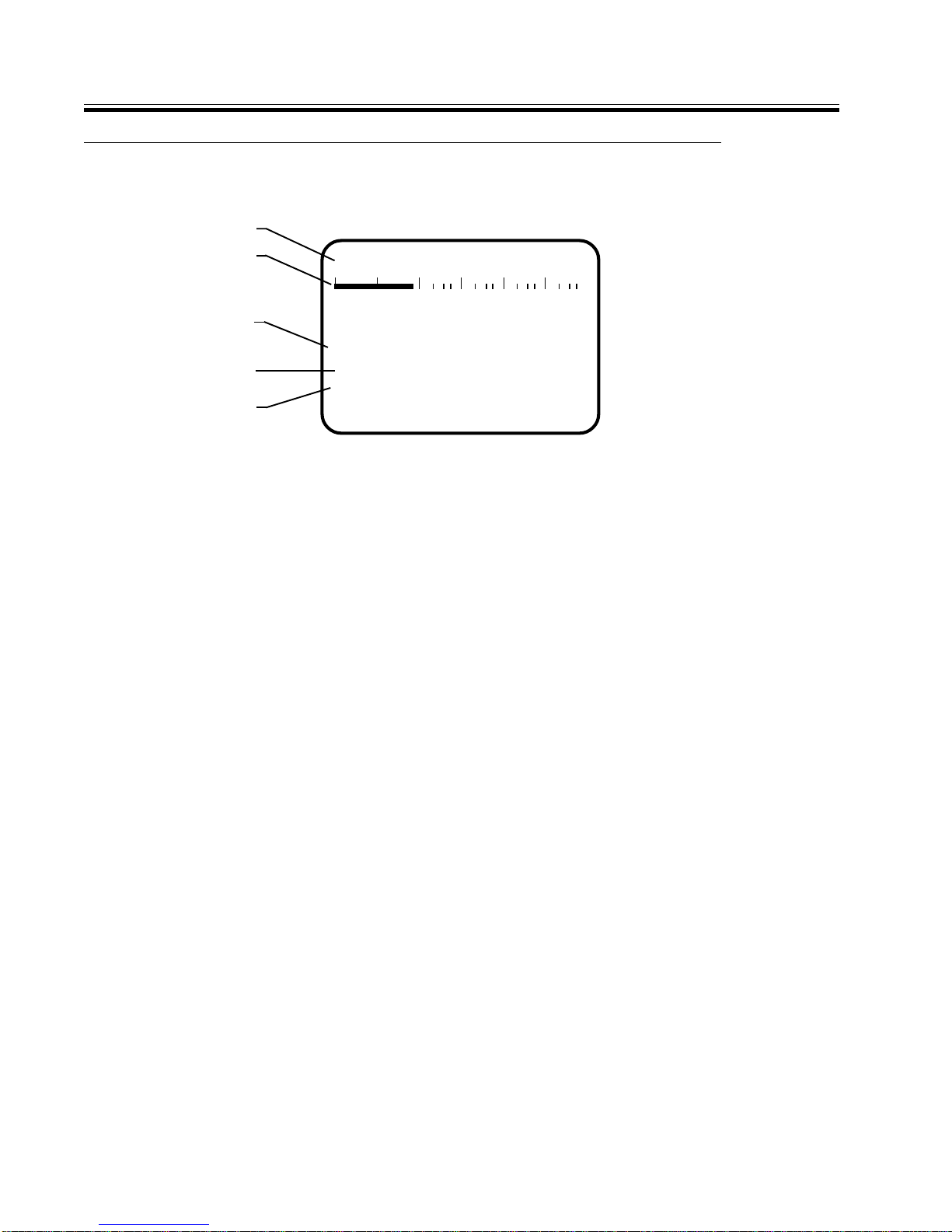
2.1 High Voltage Ramp Routine
The high voltage ramp routine is useful when a user needs to plateau a detector to
determine the proper operating voltage of the detector . The following display will appear when
performing the routine.
A
B
PROCEED W/
0
SEC
10
HV?
SCL
SCL
E
F
G
CURRENT HV = 800
C
D
STR
END
OPR CNT = 0
INC
000
H
I
HIGH VOLTAGE RAMP ROUTINE DISPLAY
A. INFORMATION PROMPT: Prompts the user for the parameters required for the ramping
routine. When the routine is first started the prompt will ask if the user wants to proceed
with the current parameters. If answered YES the instrument will then prompt the user to
begin the routine by ex ecuting the scaler count command. If answered NO then the follo wing
information prompts will appear immediately after the one before is answered.
Starting HV ?
Ending HV?
HV Increment?
The message DUMPING HEADER will then appear momentarily followed by the command
"Ent C to start".
B. RATEMETER BARGRAPH DISPLAY: A logarithmic display of the ratemeter reading in
cps.
C. HV IDENTIFIER: Identifies the current HV setting.
D. STR: Identifies the starting voltage of the HV ramping routine.
E. SCALER COUNT: Shows the scaler reading in progress.
F . SCALER TIMER: Shows the count time for the scaler . When a count is in progress the timer
will show the time remaining in the count.
G. END: Identifies the ending HV setting for the ramping routine.
H. INC: Identifies the increment the voltage will be increased by in each step of the routine.
I. OPR CNT: Identifies the count at the beginning knee of the plateau or the recommended
operating voltage.
8

MODEL 2350-1 Data Logger
2. CALIBRATION ROUTINES
The following example demonstrates how to run a plateau on a Model 44-2 Gamma
Scintillator.
KEYSTROKES
Note: Before perf orming the SHR(x) command, certain parameters must be set. The parameters
that need to be set include the threshold, window position, and count time.
RESPONSE
SHR(x) ENTER
Where (x) = the number 0 or 1.
0 = Disables data dump to the serial port.
1 = Enables data dump to the serial port.
N ENTER
500 ENTER
1000 ENTER
25 ENTER
The Model 2350 display will show the detector
display with the current set of detector parameters.
There will be no prompt but you will need to select
a set of parameters to use in the routine. If the
current parameters are correct press "Y ENTER",
otherwise select the set of detector parameters
that you want to use and then press "Y ENTER".
The instrument will proceed with the routine by
displaying the screen shown on the opposite page.
This answers the prompt
"PROCEED W/ HV" allowing the user to change
the parameters of the routine.
This set the beginning high voltage at 500
volts.
This sets the ending high voltage at 1000
volts.
This sets the HV increment to 25 volts.
(This increment is the amount that the high voltage
setting will change between each step of the
ramping routine.)
C ENTER
"SHR0" will run the plateau routine, determine the operating votage, but will not dump
data to the RS-232 port. "SHR1" will run the plateau routine, determine the operating voltage,
and will dump the voltage setting and scaler count at each increment of the plateau routine.
When the routine is complete the following prompt will appear:
"SAVE? HV = XXX"
"Y ENTER" will save the voltage as the operating voltage of the detector and the
instrument will return to the screen that was active prior to the exucution of the routine. "N
ENTER" will return to the screen that was active prior to the exucution of the routine without
saving the voltage.
This activates the routine by starting the
scaler counting.
9

MODEL 2350-1 Data Logger
2. CALIBRATION ROUTINES
2.2 Calibration Constant and Dead Time Calibration with Background Subtract
This routine will use a two point (low-hi) method to calculate the calibration constant
and dead time of the detector. The following displa y will appear when performing the routine.
A
B
C
LOW CAL POINT?
L CAL 0.000e+00
D
H CAL 0.000e+00
LO SMPL 0
E
F
HI SMPL 0
CALIBRATION CONSTANT/DEAD TIME ROUTINE DISPLAY
A. INFORMATION PROMPT: Prompts the user for the parameters required for the routine.
When the routine is first started the prompt will prompt the user low calibration point. Once
entered it will prompt for the following parameters in order.
HI CAL POINT
TAKE BACKGROUND
TAKE LOW SAMPLE
TAKE HI SAMPLE
SAVE NUMBERS?
B. RATEMETER BARGRAPH DISPLAY: A logarithmic display of the ratemeter reading in
cps.
C. L CAL: Identifies the low calibration point that will be used in the routine.
D. H CAL: Identifies the high calibration point that will be used in the routine.
E. LO SMPL: Shows the reading obtained from the low sample source.
F. HI SMPL: Shows the reading obtained from the high sample source.
NOTE: Line 1 will indicate the ratemeter reading when a sample is being tak en,
and lines 3 and 4 will show the scaler taking a count. When the routine is
complete Line 3 will display the calculated calibration constant, and line
4 will show the calculated dead time constant. These numbers will be
saved into the activ e detector setup if the user answers y es to the prompt
to save the numbers.
10

2. CALIBRATION ROUTINES
The following example will calculate the cal constant and dead time of a Model 44-2
Gamma Scintillator in R/hr.
MODEL 2350-1 Data Logger
KEYSTROKES
SKB ENTER
5e-4 ENTER
15e-3 ENTER
C ENTER
C ENTER
RESPONSE
The Model 2350-1 will show the calibration
constant/dead time routine with background
subtract control display with a prompt to set the
low cal point.
This will set the lower calibration point at
500 mR/hr, then a prompt will appear for the hi cal
point.
This will set the high calibration point at 15
mR/hr, then a prompt will appear to take a
background sample.
This will initiate the scaler to take a
background reading, then a prompt will appear to
take the low sample count. Place a 1 mCi
check source on the end of the detector.
This will initiate the scaler to take a count
with the low sample source, then a prompt will
appear for the hi sample count. Place a 5 mCi
check source on the end of the detector.
137
137
Cs
Cs
C ENTER
NOTE: The SSK command initiates the same routine as stated above except
1. The background count should be less than 2% of the low sample count.
2. The low sample count should have at least 15,000 counts.
3. The high sample should be at least 100 times the low sample and produce
This will initiate the scaler to take the hi
sample reading.
that the background count is not taken or considered when determining
the calibration constant and dead time of the system.
ADDITIONAL PARAMETERS
between 30 - 60% dead time loss.
11
MODEL 2350-1 Data Logger
2. CALIBRATION ROUTINES
2.3 Single Point Calibration Constant Routine with Background Subtract
This routine will use a single point method to calculate the calibration constant of the
detector. The following display will appear when performing the routine.
A
B
C
SINGLE CAL PT?
BACKGRND = 0
D
SAMPLE = 0
CALPT = 0.000e+00
E
CALIBRATION CONSTANT/DEAD TIME ROUTINE DISPLAY
A. INFORMATION PROMPT: Prompts the user for the parameters required for the routine.
When the routine is first started the prompt will prompt the user single calibration point.
Once entered it will prompt for the following parameters in order.
TAKE BACKGROUND
TAKE SAMPLE
SAVE CAL CNST?
B. RATEMETER BARGRAPH DISPLAY: A logarithmic display of the ratemeter reading in
cps.
C. BACKGRND: Identifies the background reading obtained during the routine.
D. SAMPLE: Identifies the sample count taken during the routine.
E. CALPT: Identifies the reference calibration point set for the routine.
NOTE: Line 1 will indicate the ratemeter reading when a sample is being tak en,
and lines 3 and 4 will show the scaler taking a count. When the routine is
complete Line 8 will display the calculated calibration constant. This
number will be saved into the active detector setup if the user answers
YES to the prompt to save the number.
12

2. CALIBRATION ROUTINES
The following example will calculate the cal constant of a Model 44-2 Gamma Scintillator
in R/hr.
MODEL 2350-1 Data Logger
KEYSTROKES
SSB ENTER
5e-4 ENTER
C ENTER
C ENTER
RESPONSE
The Model 2350-1 will show the single point
calibration constant routine with background
subtract control display with a prompt to set the
single cal point.
This will set the single calibration point at
500 mR/hr, then a prompt will appear to take a
background reading.
This will initiate the scaler to take a
background count, then a prompt will appear for
the sample count. Place the detector in a
500 mR/hr field.
This will initiate the scaler to take the single
sample reading.
NOTE: The SSS command initiates the same routine as stated above except
that the background count is not taken or considered when determining
the calibration constant.
13

MODEL 2350-1 Data Logger
2. CALIBRATION ROUTINES
2.4 Two Source Dead Time Calibration Routine with Background Subtract
This routine will use a single point method to calculate the calibration constant of the
detector. The following display will appear when performing the routine.
A
B
C
BACKGROUND
BACKGRND 0
D
E
F
SAMPLE 1 0
SAMPLE 1+2 0
SAMPLE 2 0
CALIBRATION CONSTANT/DEAD TIME ROUTINE DISPLAY
A. INFORMATION PROMPT: Prompts the user for the parameters required for the routine.
When the routine is first started the prompt will appear for the background count. Once
entered it will prompt for the following parameters in order.
SAMPLE 1
SAMPLE 1+2
SAMPLE 2
SAVE DEAD TIME?
B. RATEMETER BARGRAPH DISPLAY: A logarithmic display of the ratemeter reading in
cps.
C. BACKGRND: Identifies the background count taken during the routine.
D. SAMPLE 1: Identifies the sample count taken with source 1 during the routine.
E. SAMPLE 1 +2: Identifies the sample count taken with sources 1 & 2 during the routine.
F. SAMPLE 2: Identifies the sample count taken with source 2 during the routine.
NOTE: Lines 3 will sho w a timer and line 4 will show the word COUNTING when
a count is in progress. When the routine is complete Line 3 will display
the calculated dead time for the detector. This number will be saved into
the active detector setup if the user answers YES to the prompt to save
the number.
14

2. CALIBRATION ROUTINES
The following example will calculate the dead time of a Model 44-2 Gamma Scintillator
in R/hr.
MODEL 2350-1 Data Logger
KEYSTROKES
SSD ENTER
C ENTER
C ENTER
C ENTER
C ENTER
RESPONSE
The Model 2350-1 will show the dead time
calibration routine with background subtract control
display with a prompt to take a background
reading.
This will initiate a count to get a background
sample, then a prompt will appear to take a reading
from sample 1.
This will initiate count for sample 1, then a
prompt will appear for a count with samples 1 & 2.
This will initiate a count of samples 1 & 2
together, then a prompt will appear for a count
with sample 2 only.
This will initiate a count of sample 2 only.
ADDITIONAL PARAMETERS
1. The sources used for this test should be approximately the same size and
each should provide a minimum of 25,000 cpm.
2. When combined the sources must provide a between 25 - 60% dead time
loss.
15

MODEL 2350-1 Data Logger
3. THEORY OF OPERATION
3.1 AMPLIFIER/POWER SUPPLY BOARD #5371-002
3.1.1 INPUT
Negative going pulses are coupled from
the detector through C9 to emitter follower Q1.
CR6 is a voltage reference which provides a bias
voltage of approximately +3.3 Vdc to Q1 via R45.
R9 protects Q1 from input inadvertent shorts/
transients. R40 couples the detector to the high
voltage supply (HV).
3.1.2 AMPLIFIER
U3 is a self-biased amplifier which
provides gain in proportion to R12 divided by the
series combination of R11 and R10. R10 is
adjusted to provide a pulse height in proportion to
a given threshold setting at comparator U4
(typically adjusted to trigger with a detector input
pulse of 10 millivolts at a threshold setting of 100).
Transistor (pins 4, 5, and 6 of U3) provide
amplification and pulse polarity inversion.
Transistor pins 10 through 15 are coupled as a
constant current source to pin 6 of U3. The output
self-biases to 2 Vbe — approximately 1.4 Vdc at
pin 7 of U3. This provides just enough bias current
through pin 6 to conduct all of the current from the
constant current source. Positive pulses from pin
7 are coupled to the Window and Threshold
comparators, U4.
3.1.3 WINDOW/THRESHOLD
Threshold (THR) comparator, pins 5, 6,
and 7 of U4, provides the lower pulse height
discrimination. Pulses are AC coupled from
amplifier U3 via C23 to pin 6 of U4. THR reference
voltage data from the microprocessor board (µP)
is processed by digital to analog convertor (DAC)
U6 and coupled to pin 5 of U4 via opamp U5. R54
and C13 provide additional filtering of the
reference voltage. THR reference Vdc is approx.
+122 millivolts (mV) with the THR set at 100 on
display — 1.222 Vdc at a THR setting of 1000. As
the pulse height at pin 6 of U4 increases above the
reference
voltage at pin 5, pin 7 — normally high (approx. +5
Vdc) goes low for the pulse duration.
Window (WIN) comparator, pins 1, 2, and
3 of U4 provide the upper pulse height
discrimination. Pulses are coupled from amplifier
U3 to pin 2 of U4. WIN reference voltage data from
the µP is processed by DAC U6 and coupled to pin
3 of U4. Q2 applies approx. +5 Vdc to the WIN
reference to disable the WIN comparator when
the WIN OFF signal is applied to the base of Q2.
The WIN reference voltage rides on top of the
THR reference — i.e., with a THR and WIN setting
of 100, the WIN reference at pin 3 of U4 will equal
approx. +122 mV referenced above the THR at
pin 5 or approx. +244 mV referenced to chassis
ground. If the THR is increased to 200 and the
WIN still remains at 100 the WIN reference will still
equal approx. +122 mV referenced to the
threshold but will increase to approx. +366 mV
when referenced to ground (THR = 244 mV + 122
mV WIN = 366 mV). As the pulse amplitude
increases above the WIN reference voltage, pin 1
of U4 goes low for the pulse duration.
3.1.4 WINDOW/THRESHOLD LOGIC
CIRCUIT
Negative pulses from the THR comparator
are coupled to univibrator U9. Negative, pulses
(approx. 5 volt) are present at univibrator output
pin 7 of U9 (PULSE’) as long as pins 13 and 3
remain high. When a WIN pulse is present at pins
13 and 3 the Reset function is enabled which
disables the PULSE’ output locking pin 7 high.
Pulses are connected from pin 7 to the µP on the
Central Processor Board for count processing.
Pin 7 is tied back to pin 13 via CR1 to provide a
time delay (approx. 8 to 10 µs) for the µP clock
cycle to complete before the next pulse can be
recognized by the micro-processor.
16

3. THEORY OF OPERATION
MODEL 2350-1 Data Logger
3.1.5 DIGITAL TO ANALOG CONVERTORS
U6 and U7 are digital to analog convertors
(DAC) which convert the digital data from the µP to
analog signals to control the THR, WIN, High
Voltage Reference (HV REF), and Overload
Reference (OVR REF) variables. Data via BUS0BUS3 and A0-A2 is loaded into the DAC latches
for U6 and U7 by strobing CE3' and CE4' (Chip
Select). CE5' (Up Date) is then strobed to transfer
the data stored in the latches to the DAC outputs.
3.1.6 HIGH VOLTAGE SUPPLY AND
DETECTOR OVERLOAD
Detector High Voltage (HV) is developed
by blocking oscillator Q3, T1, C29 and rectified by
voltage multiplier CR3-CR5, CR14, CR15, C5,
C32, C37, and C38. Q4, CR13, and R41 provide
a regulated voltage of approx. 4.4 Vdc (battery
voltage must be +4.4 Vdc) to the emitter of Q3.
HV increases as current through Q5 increases
with maximum output voltage with Q5 saturated.
HV is coupled back through R5, through
voltage follower U1, to pin 6 of U2 to complete the
regulation loop. Resistors R52 and R6 complete
the HV divider network to ground. HV regulation is
produced by opamp comparator pins 5, 6, and 7 of
U2. During stable operation the voltage at pin 6 will
equal pin 5. If HV REF is increased, pin 7 of U2
will increase increasing conduction of Q5 until the
voltage at pin 6 equals pin 5 of U2 via HV divider
network, R5, R52, and R6. R52 is adjusted to
calibrate the HV output to the HV REF signal
supplied to pin 5 of U5 by the DAC — HV REF is
set at approx. 1500 mV by entering the “H1500"
command into the Model 2350-1, the HV CAL is
adjusted for 1500 Vdc at the detector connector.
C1-C3, C8-C7, C19, and C27 provide additional
filtering of the HV output.
Detector Overload is achieved by
measuring the voltage differential across R4. As
current is increased into the detector, a voltage
drop is produced across R4. The HV on either side
of R4 is converted to a low voltage by resistor
divider networks R5, R52, R6, and R44, R7, and
R43. The voltage differential is coupled to
differential opamp, pins 12-14 of U1, via opamp
buffers. The differential output is coupled to
opamp comparator, pins 8- 10 of U1. OVR REF is
provided by the µP via the DAC — OVERLOAD’ is
coupled back to the µP. R7, CURRENT CAL,
calibrates the detector current drain to the OVR
REF input — i.e., a 10µA load is connected to the
detector output; the overload is set to “100" by
entering the “O100" command (approx. 610mV at
OVR REF), R7, CURRENT CAL, is then adjusted
until pin 8 or U1 just starts to trigger low.
3.1.7 LOW VOLTAGE SUPPLY
Supply voltages of +5 and -10 Vdc are
supplied by U8, T2, and supporting components.
U8 is a switching regulator with an on-board
comparator providing regulation. An internal
voltage reference of 1.0 Vdc maintains the
inverting and non-inverting comparators at 1.0V
via the feedback loop. Oscillator frequency, set by
C36, is approx. 100 kHz at pin 5 of U5. CR11 and
C26 provide rectification and filtering for the +5V
output. CR12 and C25 provide rectification and
filtering for the -10V output.
U11 is a -2.5 Vdc voltage reference for the
DAC’s — U6 and U7. C8 located on the Backplane
board maintains the battery voltage charge during
inadvertent battery disconnection (mechanical
shock).
3.1.8 LCD VIEWING ANGLE SUPPLY
U2 is configured as a differential opamp
which controls the backplane voltage to adjust the
viewing angle for the LCD graphics display.
Output voltage, pin 1 of U2 is adjustable from 0 to
-10 Vdc by varying R50 (VIEWING ANGLE). LCD
backplane variance due to temperature is
compensated by CR10.
17

MODEL 2350-1 Data Logger
3. THEORY OF OPERATION
3.2 CENTRAL PROCESSOR BOARD #5371-068
3.2.1 MICROPROCESSOR (µP)
U124, Intel 80C51FA, is the Model 2350-1
central processor. The µP clock frequency is
crystal controlled by Y159 and related components
at 6.144 MHZ. C172 resets the µP at power-up to
initiate the start of the program routine. The main
program routine is stored in EPROM, U122. User
parameters and logged data is stored in the 8k X
8 RAM, U123. (replaced with 64k X 8 RAM located
on the Memory Expander board)
Address and data information are
multiplexed by latch U121 from the µP to the two
memory chips. The low address bits A0-A7 are
multiplexed with the data bus, BUS0-BUS7, out of
the µP. U121 latches the address data AO-A7 on
lines BUS0-BUS7 during the first part of the
external memory cycle when the ALE input is
strobed.
The HD175 ACCESS shunt configures the
µP parameter access mode and password. When
pins 1 and 2 are shunted (default) the access
parameters is determined by the settings preset in
the EPROM and the password entered in RAM. If
shunt is placed between pins 2 and 3 the
password is set to “0" and the access level is set
to “3".
The ACKNOWLEDGE’ input is pulled low
when the front panel ACKNLDGE pushbutton
switch is depressed silencing the audible
alarm(s). The OVERLOAD’ signal from the AMP/
PS board instructs the µP to initiate an
OVERLOAD condition. WIN OFF’ is an output
signal from the µP to the AMP/PS board which
disables the Window feature.
The TONE’ input comes from the I/O
processor which toggles the TONE’/ALARM line
low when the external bar code wand registers bar
code information. The TONE’ and ALARM’ (µP
output signal from pin 5 of U124) signals initiate an
independent audible tone by changing the CV
(control voltage) input on the ICM7556 timer,
U118.
The READY, CLEAR SEND, RECEIVE,
and XMIT data lines communicate the RS-232
and bar code reader wand information from/to the
I/O processor to/from the central processor. The
RESET output at pin 13 of U124 is coupled to the
I/O board to reset the I/O processor. Q174 inverts
the RESET signal (RESET’) providing a reset line
for the LCD graphics display. The PULSE’ input
supplies the pulses from the AMP/PS board to be
counted and converted into data by the µP.
3.2.2 BATTERY VOLTAGE VFC
Un-switched (connected directly to
batteries) battery voltage — +BATUNS — is
divided by resistor divider network R148 and R149
and connected to voltage to frequency convertor
(VFC), U125. VFC OUT is connected to a counter
inside the µP which counts the frequency for a
preset time converting to a number displayed on
the LCD representing the battery voltage. R130,
BAT CAL, adjusts the VFC frequency output to
calibrate the LCD BAT reading to the actual
battery voltage.
NOTE: Disregard sections 3.2.3 and 3.2.4 for the
Model 2350-1
3.2.3 RECORDER DRIVE CIRCUIT
The RCDR output from the µP is coupled
to MOSFET transistor Q126. The µP uses pulsewidth modulation for the recorder signal. The
pulse-modulated signal is integrated by R144 and
C100. Pins 5, 6, and 7 of U126 “buffers” the
integrated voltage from R131. R131 provides
calibration of the recorder output voltage. Pins 1,
2, and 3 of U126 are configured as an opamp
voltage follower providing recorder drive.
3.2.4 ADDRESS DECODER/VOLTAGE
BACKUP
U120 is address decoder which generates
the chip enable signals — CEO-CE7 — by
monitoring address lines A13-A15. U120 also
provides battery backup, +5VBACK, to the Clock
chip U119 and the RAM U123. This enables the
user to change the instrument batteries without
losing RAM memory. +BATUNSR supplies
battery voltage to CR112 voltage reference to limit
the voltage at 5.1 Vdc. The 5.1 Vdc is coupled to a
0.1
18

3. THEORY OF OPERATION
MODEL 2350-1 Data Logger
3.3 I/O INTERFACE BOARD #5371-063
farad capacitor through CR113. CR113 prevents
C129 from discharging through the +BATUNSR
line when the batteries are removed.
3.2.5 CLOCK CHIP
U119 provides the time and date
information used in conjunction with the logged
data. U119 is crystal controlled by Y158 and
supporting components C102 and C103 at
32.786 kHz. The 10 Hz output at pin 13 of U119,
provides the timing frequency to the µP.
3.2.6 AUDIO CIRCUIT
Pulses are coupled from the AMP/PS
board to U128 — RDD 104 decade divider chip.
AUDIO DIVIDE (front panel) by “1" switch position
jumpers the PULSE’ input directly to the CLICK’
input to the timers. Divide by “10" and “100" switch
positions connect the DIV OUT of U128 to the
CLICK’ input using U128 for pulse division. U118,
a dual package 7555 timer, provides audio
oscillation. Pulses (CLICK’) are coupled to the first
timer, pins 1-6 of U118, via C97. This timer is
configured as a monostable multivibrator (oneshot) producing a fixed pulse-width for each input
pulse at pin 6 of U118. Pulse-width is set by R161
and C95. CR114 limits pulse input to pin 6 of U118
to 5.6 volts; R134 is a pull-up resistor for the AC
coupled pulse. The second half of U118 is
configured as a astable (free-running) multivibrator
which produces the audible tone — frequency is
set by R133 and C96.
T157 provides amplification of the audio
signal driving the unimorph speaker. Audio
volume is varied by adjusting the voltage on top of
the primary winding of T157 via the front panel
volume control. When an ALARM’ is initiated
maximum voltage applied by saturating Q154.
3.3.1 MICROPROCESSOR (µP)
U15, Intel 80C51FA, communicates and
processes information bi-directionally from/to the
RS-232 interface (U13) to/from the central
processor via the serial interface lines XMIT,
READY, RECEIVE, and CLEAR SEND. U15 also
decodes information from the bar code reader
(WAND) and sends information to central
processor. The µP clock frequency is crystal
controlled by Y159 and related components at
6.144 MHZ.
U14, EPROM, stores the program for the
I/O µP. U14 incorporates on-board latches to
separate the multiplexed address and data buss
lines.
CR26-CR28 provide “clipping” of transients
which may be produced at the SERIAL I/O port.
3.3.2 RS-232 INTERFACE
U13, MAX232, is a +5 Vdc powered RS232 driver/ receiver used to interface the Model
2350-1 to a computer or keypad terminal. U13
incorporates on-board voltage multipliers which
generate the +10 and -10 volts required for RS232 communication.
3.3.3 BACKLIGHT DRIVE
The LCD backlight is illuminated by
appling power to +EL POWER when front panel
BACKLIGHT switch is ON. With battery voltage
applied to +EL POWER, blocking oscillator —
Q23, T1 and supporting components begin
oscillating. The signal is amplified by T1 to provide
a 70VAC signal to drive the LCD backlight. R30,
a 10 ohm resistor, limits the power-up surge to the
oscillator circuit.
19

MODEL 2350-1 Data Logger
3. THEORY OF OPERATION
3.4 64k MEMORY EXPANDER BOARD #5371-054
NOTE: When the MEMORY EXPANSION board
is added, U120 (DS1211) and U123 (CDM6264)
on the CENTRAL PROCESSOR board must be
removed. The red entries in the CENTRAL
PROCESSOR theory of operation should be
removed/or inserted for the M2350-1.
U119 is a 128k RAM (only 64k is used) used to
store user parameters and logged data. U119 is
selected by the central µP by applying a logic
“high” to the RAM input, Pin 30 of U119. The
Recorder circuit is disabled on the Central
Processor board and the RCDR output on the
central µP is used to enable the Memory
Expansion board RAM.
U117 is address decoder which generates the
chip enable signals — CE1-CE7, E1 — for the
DAC’s on the AMP/PS board and the Clock chip
on the Central µP board by monitoring address
lines A12-A14 from the central µP.
U115 provides battery backup, +5VBACK, to
the Clock chip (U119) on the Central µP board and
the RAM. This enables the user to change the
instrument batteries without losing the RAM
memory. U115 also provides a RESET signal
which goes low when the +5V supply to pin 2 of
U115 drops below a preset threshold (4.5-4.75
volts). This opens U116 analog switches
disabling the RAM and CLOCK’ signals from the
data bus to save the parameter and logging
memory.
20

MODEL 2350-1 Data Logger
4. PARTS LIST, COMPONENT LAYOUTS, AND SCHEMATICS
AMPLIFIER / POWER SUPPLY BOARD
Ref. No.
CAPACITORS
C1-C3
C4
C5
C6-C8
C9
C10
C11-C12
C13
C14
C15
C16
C17
C18-C19
C20-C21
C22
C23
C24
C25
C26
C27
C28
C29
C30
C31
C32
C33
C34
C35-C36
C37-C38
C39
C40
C41
C42
Description
0.0056mF, 3kV
0.1 mF
0.0015 mF, 3kV
0.0056 mF, 3kV
100 pF, 3kV
10 mF
100 pF
0.01 mF
47 pF
100 mF
220 pF
100 pF
0.0056 mF, 3kV
33 pF
0.01 mF
0.1 mF
0.0056 mF, 3kV
22 mF
220 mF
0.0056 mF, 3kV
100 pF, 3kV
0.01 mF
100 mF
100 pF
0.0015 mF, 3kV
33 pF
1 mF
0.001 mF
0.0015 mF, 3Kv
10 mF
0.1 mF
33 pF
0.01 mF
Part No.
04-5522
04-5521
04-5518
04-5522
04-5532
04-5592
04-5527
04-5523
04-5533
04-5576
04-5530
04-5527
04-5522
04-5616
04-5523
04-5521
04-5522
04-5579
04-5639
04-5522
04-5532
04-5523
04-5576
04-5527
04-5518
04-5616
04-5575
04-5519
04-5518
04-5592
04-5521
04-5616
04-5523
DIODES
CR1-CR2
CR3-CR5
CR6
CR7
CR8-CR10
CR11-CR12
CR13
1N4148
MR250-2
1N5226
1N5819
1N4148
1N5819
1N4148
21
07-6272
07-6266
07-6260
07-6306
07-6272
07-6306
07-6272

MODEL 2350-1 Data Logger
4. PARTS LIST, COMPONENT LAYOUTS, AND SCHEMATICS
Ref. No.
DIODES
CR14-CR15
CR16-CR18
TRANSISTORS
Q1
Q2
Q3
Q4
Q5
RESISTORS
R1
R2
R3
R4
R5
R6
R7
R8
R9
R10
R11
R12
R13-R14
R15
R16
R17-R19
R21
R22
R23
R24
R25
R26
R27
R28
R29
R30
R31
R32
R33-R36
R37
R38
Description
MR250-2
1N4148
2N3904
MPS6534
MPS-U51
MPS-U01
2N3904
10kohm, 333MW
47 ohm, 333MW
56 kohm, 333MW
4.7 Mohm
1 Gohm
470 kohm, 333MW
1 Mohm, pot
100 kohm, 333MW
10 kohm, 333MW
100 kohm, pot
1 kohm, 333MW
470 kohm, 333MW
10 kohm, 333MW
1 kohm, 333MW
4.7 kohm, 333MW
10 kohm, 333MW
0.1 ohm, 3W
80.6 kohm, 333MW
1 Mohm, 333MW
10 Mohm, 333MW
10 kohm, 333MW
80.6 kohm, 333MW
62 kohm, 333MW
1 Mohm, 333MW
33.2 kohm, 333MW
47 kohm, 333MW
100 ohm, 333MW
221 kohm, 333MW
10 kohm, 333MW
820 ohm, 333MW
10 kohm, 333MW
Part No.
07-6266
07-6272
05-5755
05-5763
05-5765
05-5778
05-5755
12-7748
12-7756
12-7789
10-7030
12-7686
12-7757
09-6828
12-7747
12-7748
09-6823
12-7750
12-7757
12-7748
12-7750
12-7755
12-7748
12-7647
12-7762
12-7763
12-7749
12-7748
12-7762
12-7790
12-7763
12-7793
12-7758
12-7746
12-7792
12-7748
12-7791
12-7764
22

MODEL 2350-1 Data Logger
4. PARTS LIST, COMPONENT LAYOUTS, AND SCHEMATICS
Ref. No.
RESISTORS
R39-R40
R41
R42
R43
R44
R45
R46
R47
R48
R49
R50
R51
R52
R53
R54
R55
R56
R57
R58
R59
Description
1 Mohm
100 kohm, 333MW
3 kohm, 333MW
470 kohm, 333MW
1 Gohm
100 kohm, 333MW
10 kohm, 333MW
33.2 kohm, 333MW
1 Mohm, 333MW
12 kohm, 333MW
1 kohm, pot
330 ohm, 333MW
1 Mohm, pot
22 kohm, 333MW
10 kohm, 333MW
1 kohm, 333MW
1 Mohm, 333MW
80.6 kohm, 333MW
1 Mohm, 333MW
10 kohm, 333MW
Part No.
10-7028
12-7747
12-7768
12-7757
12-7686
12-7747
12-7748
12-7793
12-7763
12-7787
09-6831
12-7788
09-6828
12-7754
12-7748
12-7750
12-7763
12-7762
12-7751
12-7748
RESISTOR NETWORK
RN1
RN20
TRANSFORMERS
T1
T2
INTEGRATED CIRCUITS
U1
U2
U3
U4
U5
U6-U7
U8
U9
U10
U11
5.6 kohm
220 kohm
M2350-1 HVPS
M2350-1 LVPS
LT1079
LT1078
CA3096
TLC372
LT1078
AD7549
LM2578
CD4098
LT1078
LM385Z
12-7696
12-7578
4275-037
4275-089
06-6252
06-6251
06-6023
06-6265
06-6251
06-6253
06-6223
06-6066
06-6251
05-5791
23

MODEL 2350-1 Data Logger
4. PARTS LIST, COMPONENT LAYOUTS, AND SCHEMATICS
CENTRAL PROCESSOR BOARD
Ref. No.
CAPACITORS
C95
C96
C97
C98
C99-C100
C101
C102-C103
C104
C109
C110
C111
C129
C172
C177
DIODES
CR112
CR113-CR115
CR162
Description
0.047 mF
0.001 mF
47 pF
0.01 mF
0.1 mF
27 pF
22 pF
27 pF
10 mF
100 mF
1 mF
0.1 F
10 mF
0.1 mF 100V
1N5231
1N4148
1N4148
Part No.
04-5565
14-5519
04-5533
04-5523
04-5521
04-5614
04-5552
04-5614
04-5592
04-5576
04-5575
04-5633
04-5592
04-5521
07-6261
07-6272
07-6272
HEADER
HD175
TRANSISTORS
Q153
Q154
Q155
Q168,Q174
RESISTORS
R130
R131
R132
R133
R134
R135
R137-R138
R139
R140
R141-R142
R143
3 PIN SIP
2N3904
MPS6534
2N3904
2N7000
10 kohm, pot
100 kohm, pot
2.2 kohm
470 kohm
220 kohm
5.6 kohm
10 kohm
33 kohm
10 kohm
100 kohm
7.15 kohm
n/a
05-5755
05-5763
05-5755
05-5820
09-6822
09-6823
10-7012
10-7026
10-7066
10-7042
10-7016
10-7019
12-7540
12-7557
12-7620
24

MODEL 2350-1 Data Logger
4. PARTS LIST, COMPONENT LAYOUTS, AND SCHEMATICS
Ref. No.
RESISTORS
R144
R148
R149
R160
R161
R164
R166-R167
R170
R176
RESISTOR NETWORKS
RN151
TRANSFORMERS
T157
INTEGRATED CIRCUITS
U118
U119
U120
U121
U122
U123
U124
U125
U126
U128
Description
1 Mohm
35.7 kohm
8.66 kohm
220 kohm
150 kohm
1 Mohm
10 kohm
1 Mohm
220 kohm
22 kohm
M2221, 300-9
ICM7556
MM58274
CPL-200-T2-T
CD74HC573
27C512
CPL-140-T2-T
80C51FA
LM331
TLC27M71P
RDD104
Part No.
10-7028
12-7640
12-7623
10-7066
10-7024
10-7028
12-7540
10-7028
10-7066
12-7566
4275-074
06-6244
06-6254
06-6441
06-6093
06-6264
06-6439
06-6236
06-6156
06-6248
06-6060
CRYSTALS
Y158
Y159
32 kHz XT AL
6.144 MHz XT AL
25
01-5219
01-5212

MODEL 2350-1 Data Logger
4. PARTS LIST, COMPONENT LAYOUTS, AND SCHEMATICS
64k MEMORY EXPANDER BOARD
Ref. No.
RESISTORS
R001
R114
INTEGRATED CIRCUITS
U115
U116
U117
U119
Description
22.1 kohm
221 kohm
MAX703ESA
CD74HC4066M
CD74HC138M
CXK581000M
Part No.
12-7843
12-7845
06-6381
06-6323
06-6339
06-6385
26

MODEL 2350-1 Data Logger
4. PARTS LIST, COMPONENT LAYOUTS, AND SCHEMATICS
I/O INTERFACE BOARD
Ref. No.
CAPACITORS
C3-C4
C5
C6
C8-C11
C12
C37-C39
RESISTORS
R16
R19
R20-R21
R30
R40
RESISTOR NETWORKS
RN33
DIODES
CR26-CR28
Description
27 pF
0.047 mF
100 mF
10 mF
4.7 mF
220 mF
33 ohm
8.2 kohm
3.3 kohm
10 ohm
4.7 ohm
10 kohm
1N5231
Part No.
04-5614
04-5565
04-5576
04-5592
04-5578
04-5639
10-7001
10-7015
10-7013
10-7046
10-7095
12-7777
07-6261
TRANSISTORS
Q23
TRANSFORMERS
T1
INTEGRATED CIRCUITS
U13
U36
CRYSTALS
Y25
2N3904
M2350-1 EL
MAX232
87C51FA
6.144 MHz MICRO XTAL
05-5755
4275-090
06-6188
06-6405
01-5212
27

MODEL 2350-1 Data Logger
4. PARTS LIST, COMPONENT LAYOUTS, AND SCHEMATICS
BACKPLANE BOARD
Ref. No.
RESISTORS
R6
DIODES
CR5
CR7
CONNECTORS
J1-J2
Description
1 kohm
1N4148
1N5819
125X44-CBNEARS
EZA22DRSN
Part No.
10-7009
07-6272
07-6306
13-8181
28
 Loading...