

Page 1

5GXM
AT Form Factor
Main Board
User's Manual
Page 2

Copyright
Copyright © 1998 by this company. No part of this document may
be reproduced, transmitted, transcribed, stored in a retrieval system,
or translated into any language or computer language, in any form or
by any means without prior written permission. This manual and the
information contained herein are protected by copyright. All rights
reserved.
Manual version: 1.0
Published in 1998
Page 3

Warning and disclaimer
This manual is designed to provide information about the
Pentium® system board. Every effort has been made to make this
manual as accurate as possible, but no warranty or fitness is implied.
All the information is provided on an 'as is' basis. The author and his
corresponding publishing company shall have neither liability nor
responsibility to any person or entity with respect to any loss or
damages arising from the information contained in this manual or
from the use of the system board that accompanies it.
Information contained in this manual is subject to change without
notice. The manufacturer of the main board will not be held
responsible for technical or editorial omissions made herein, nor
for the incidental or consequential damages resulting from its
furnishing, performance, functionality or use. Subsequent changes
to this manual will be incorporated into the next edition. We
welcome any suggestion regarding this manual or our computer
products.
Trademarks
Intel and Pentium are registered trademarks of Intel Corporation.
•
IBM is a registered trademark of International Business Machines
•
Corporation.
Microsoft is a registered trademark of Microsoft Corporation.
•
PCI is a registered trademark of PCI Special Interest Groups.
•
AWARD is a registered trademark of Award Software Inc.
•
All other trademarks are the property of their respective owners.
Page 4

Table of contents
Chapter 1 Introduction…………...………………...…
1-1 5GXM Main Board Overview….……………………………………..
1-2 Specifications……………………………………………………….…
1-3 Cyrix Cx5530 & MediaGXm Overview……………………………….
1-4 System Block Diagram…………………………………………………
1-5 Notice of Hardware Installation………………………………………..
1-6 Notice of CD Driver Installation……………………………………….
Chapter 2 Installation…………………………….……
2-1 Layout Reference……………………………………………………
2-2 Quick reference to CPU Speed Setup…………………………
2-3 Jumper Settings……………………………………………………….
2-3-1 JP1:Flash ROM Voltage Selector…………………………10
2-3-2 JP5: CMOS Status Selector…………………………………11
2-3-3 JP6: CPU Ratio Selector……………………………………12
2-4 Connectors……………………………………………………………
2-4-1 Front Panel Connectors……………………………………13
2-4-2 Back Panel Connectors………………………………………15
COM 1/COM2……………………………………………………………….
LPT1……………………………………………………………….…….…
USB1…………………………………………………………………..………
AT Keyboard ………………………………………………………………
PS/2 Mouse………………………………………………………...…….
2-4-3 ATX Power Supply Connector………………………………19
2-4-4 AT Power Supply Connector……………………………...…20
2-4-5 IR1 Connector………………………………………………..21
2-4-6 FAN1 Connector……….……………………………………..22
2-4-7 FDC1: Floppy Interface…………………………………..23
2-4-8 IDE 1 and IDE2………………………………………………24
2-4-9 J1: CD-IN…………………………………………………..…25
2-4-10 J2: Multi-media Connector…………………………………25
2-4-11 Wake Up On LAN…………………………………………27
2-4-12 Game Port…………………………………………………...28
2-5 DIMM Memory Installation…….…………………….…………....…
8
.9
16
17
18
1
1
2
4
5
6
7
8
10
13
15
17
29
II
Page 5

Chapter 3 BIOS Setup..……...………….. …………
3-1 Award BIOS CMOS Setup……………………………………………
3-2 Standard CMOS Setup………………………………………………
3-3 BIOS Features Setup…………………………………………………
3-4 Chipset Features Setup…………………………………………...
3-5 Power Management Setup…………………………………………....
3-6 PNP/PCI Configuration Setup……………………………………
3-7 Integrated Peripherals………………………………………………
3-8 Supervisor/ser Password…………………………. …………………
3-9 IDE HDD Auto Detection…………………………………………….
3-10 Load Setup Defaults…………………………………………………..
3-11 Save and Exit Setup…….. ……………………….. ………………….
3-12 Quit Without Saving……………………….. ………………………...
Chapter 4 Appendix…………………….…………….
4-1 Memory Map………………………………………………….…...…
4-2 I/O Map…………………………………………………………..…...
4-3 Time & DMA Channels Map…………………………………………
4-4 Interrupt Map………………………………………….. ……. ….…..
4-5 RTC & CMOS RAM Map……………………………………………
4-6 Award BIOS Hard Disk Type………………………………………...
4-7 ISA I/O Address Map…………………………………. …………....
Chapter 5 Q & A……………..…………………………
5-1 Error Messages During Power On Self Test …………………..……..
5-2 Web-site Service………………………………………….…………..
30
37
40
42
30
31
33
38
46
49
52
53
54
55
55
56
57
58
59
60
62
64
64
66
III
Page 6

5GXM
Chapter 1 Introduction
1-1 5GXM Main Board Overview
5GXM is designed with graphics and audio functions on board. Based on system
chipset “Cyrix Cx5530™” and MMX-enhanced MediaGx™ processor, 5GXM
integrated those functions into a main board. Cyrix MMX-enhanced MediaGX™
processor is an advanced 32-bit x86 compatible processor offering high
performance, fully accelerated 2D graphics, a 64-bit synchronous DRAM
controller and a PCI bus controller, all onto the processor.
5GXM implements high performance I/O Controller utilizes with fully Plug and
Play device which supports 2.88 MB Floppy, Dual 16550 Compatible (with 16
bytes FIFO, up to 460K baud rate) Serial Port, ECP (Enhanced Capabilities Port),
EPP (Enhanced Parallel Port ) parallel port, Infrared IrDA (HPSIR), and
Amplitude Shift Keyed IR. (ASKIR) port.
5GXM supports 2*PCI & 2*ISA for highest performance I/O add-on adapter
cards. The system board supports two PCI bus-mastering slots (PCI 2.1
compliant) and allows synchronous CPU and PCI bus clock frequency.
5GXM is also strengthened with Power Management Wake up Event such as
“WOL (Wake up on LAN),” and “Modem ring on,” which are the new
inventions to enable PCs to be turned on over the network or modem. These are
also key benefits in PC op eratio n, asset management, ne w system setup and power
conservation.
In conclusion, 5GXM is a combination of the highest in performance, flexibilility,
efficiency, and ease of use that meets a variety of price/performance levels. The
5GXM is an ideal platform for the increasing requirements of today’s and future’s
desktop application.
GXM Main Board 1
Page 7

5GXM
1-2 Specifications
•
PCB board size:
•
PCB layer:
•
ZIF Socket 7
Only support Cyrix® MediaGx™ series.
•
Cyrix® MediaGX™ series : 32-Bit x86 Processor (233 - 300 MHz)
320-pin Staggered Pin Grid Array (SPGA)
Speeds offered up to 300 MHz
MMX™ technology
FPU(Floating Point Unit)
16 KB L1 cache
Since 5GXM is especially designed based on Cyrix® MedaiGX™
CPU and Cx5530™ chipset, only Cyrix® MedaiGX™ processors
are supported by 5GXM.
• Chipset : Cyrix® Cx5530™
• Memory DIMMs
2 of 168-pin unbuffered DIMMs
Memory control/interface directly from CPU
64-bit wide memory bus
SDRAM bus frequency: 66 MHz or 100 MHz
22 cm x 21 cm
4 layers
• Expansion Slot : 2x ISA slots, 2x PCI slots
• Video functions
2D Graphics Accelerator
Display Controller
MPEG-1
TV-OUT (optional)
GXM Main Board 2
Page 8

5GXM
• BIOS
licenced A
ward® full
• I/O function
2 x PCI IDE devices
1 x FDC, 2 x serial ports(16550 fast COM.)
1x parallel port device /EPP/ECP
2x USB connector
IrDA (infrared) connector
z
AT form factor: AT/ATX power supply optional
z
Green function: Complied with APM (Advanced Power Management)
z
Electrical--- Typical power supply
Below is reference for system power supply.
Voltage Tolerance Current Power Supply
+5V
+3.3V
+12V
-5V
-12V
±5%
±5%
± 10%
±5%
±5%
PnP
(Plug & Play) BIOS, flash ROM BIOS
22 Amperes AT or ATX
3 Amperes ATX only
800 mA AT or ATX
150 mA AT or ATX
100 mA AT or ATX
WOL (Wake up on LAN) function requirement:
Power supply should offer at least 750mA to the signal “5V trickle voltage” to
support.
z
Special features
Wake up on LAN
Modem ring on
Windows 95 power off
GXM Main Board 3
Page 9

5GXM
1-3 Cyrix Cx5530™ & MediaGX™
Sy stem Chipset:
Cyrix CX 5530(TM ) Features
.PC 98 Com pliant
.P C I t o I SA Bridge
.PO W ER M anagement
.Audio Support
.Ultra DMA33
.2 * U S B
.M P EG -1
.AC 97 ver.2.0 A udio
.352BGA
CPU: Cyrix(TM) M ediaGX(TM )
All on a chip
70
w ith M M X (TM ) te ch nol og y
1. 64-bit x 86 compatible processor
2. fully accelerated 2D grap hics
w/pixel processing and rendering functions
3. 64-bit synchronous D RA M controller
4. PCI b u s co n troller
5. 16 KB y te write-back L 1 ca che
Since 5GXM is especially designed based on Cyrix® MedaiGX™
processor, only 5GXM only supports Cyrix® MedaiGX™
processpr. Using other CPUs instead of MediaGX™0 series, CPU
will be seriously burned due to incompa tibility
GXM Main Board 4
Page 10

5GXM
1-4 System Block Diagram
USB
USB
CODEC
GP/GPI
Y-U-V data
System
Chipset:
Cyrix
Cx5530
CPU:
Cyrix
R-G-B data
GXm
FP Out/Digital Port
ROM
RGB out
CONTROL
PCI Bus
IDE Bus
KBC
CRT
D<63:0>
C:>
DRAM
I/O
SUPER
Digital RGB
to NTSC
TV
GXM Main Board 5
Page 11

5GXM
1-5 Notice of Hardware Installation
Before hardware installation, make sure you have checked the following
things.
A. Check the package
If any of these items is missing or damaged, contact the dealer from whom
you purchase. Leave this main board in its original package until you are
ready to install it. In the package, there are:
5GXM main board
manual
cables (w/ a 20-pin multi-media module)
driver & utility / CD
Cyrix™ GXM CPU
Since 5GXM is especially designed based on Cyrix® MedaiGX™
processor, only 5GXM only supports Cyrix® MedaiGX™
processor . Using other CPUs instead of MedaiGX™ series, CPU
will be seriously burned due to incompa tibility
B. Make sure power is off.
C. Avoid ESD (Electrical Static Discharge).
While working with
avoid ESD (Electrical Static Discharge).
5GXM
, wear a grounded wristband or ankle strap to
GXM Main Board 6
Page 12

5GXM
1-6 Notice of CD Driver Installation
The CD contains drivers for Windows 95, Windows 98, and Windows NT for
5GXM.
Enter CD “5GXM directory” and see the below screen.
Step1:
Step 2:
Step 3:
***Windows 95/98 environment:
If the operation system is Windows 95 or Windows 98 environment, enter WIN9x
ide” directory and follow the instructions of the file
install drivers.
***Windows NT environment
If the operation system is Windows NT environment, please install “NT40audio”
and “NT40display.”
Run the icon of Cyrix MediaGX W…
Install drivers for operation system
“95_98 README”
CD driver is always updated with the latest version, so the actual CD content may
have some difference with the above picture.
to
In the CD 5GXM directory, it provides drivers for Windows 98, Windows 95, and
Windows NT
GXM Main Board 7
Page 13

5GXM
Chapter 2 Installation
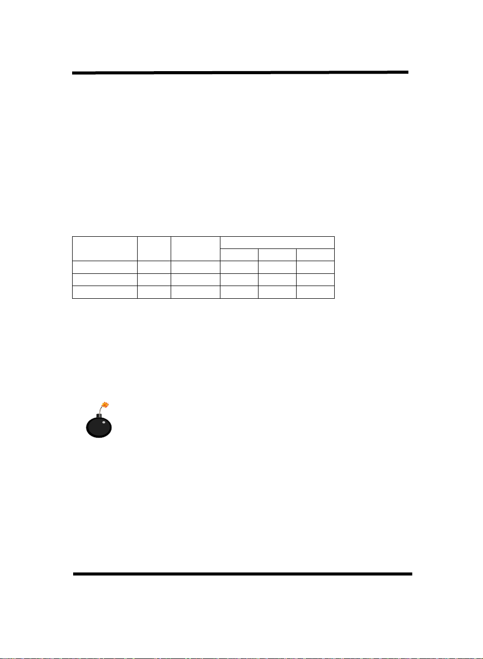
2-1 Layout Reference
CHRO N TEL
J1
J2
GAME
USB1
K/B MOUSE
AT P O W E R
AT X PO W E R
AT X PO W E R
IDE2IDE1LPT1
FDC1
ISA 2
ISA 1
JP1
BIOS
I/O
PC9731 7
J3
JP5
CYRIX
5530
IR 1
COM2 COM1
PCI2
PCI1
DIMM 2
DIMM 1
JP6
FAN1
JP7
5GXM supports Cyrix™ MedaiGX™ CPUs up to 300 MHz.
GXM Main Board 8
Page 14
5GXM
2-2 Quick Reference to CPU Speed Setup
Based on Cyrix™ MedIAGX™ processor and Cx5530 chipset, 5GXM only
supports Cyrix™ MedaiGX™ CPU up to 300 MHz. Using other CPUs instead of
Cyrix™ MedaiGX™ series, the CPUs will be seriously burned.
CPU CPU
Ratio
GX 233 MHz 7X 33.3 MHz ON OFF OFF
GX 266 MHz 8X 33.3 MHz OFF OFF OFF
GX 300 MHz 9X 33.3 MHz ON OFF ON
Since 5GXM is especially designed based on Cyrix® MedaiGX™
CPU, 5GXM only supports Cyrix® MedaiGX™ CPU. Using
other CPUs instead of MedaiGX™, CPU will be seriously burned
due to incompatibility
CPU
Frequency
JP6
1-2 3-4 5-6
GXM Main Board 9
Page 15

5GXM
2-3 Jumper Settings
2-3-1 JP1: Flash ROM Voltage Selector
JP1 is a 3-pin connector to select 5V or 12V flash ROM. Select “1-2” for 5V or
“2-3” for 12V.
JP1: Flash R O M Voltage Selector
Pin1
JP1 Flash ROM Voltage
1-2 5V
2-3 12V
GXM Main Board 10
Page 16

5GXM
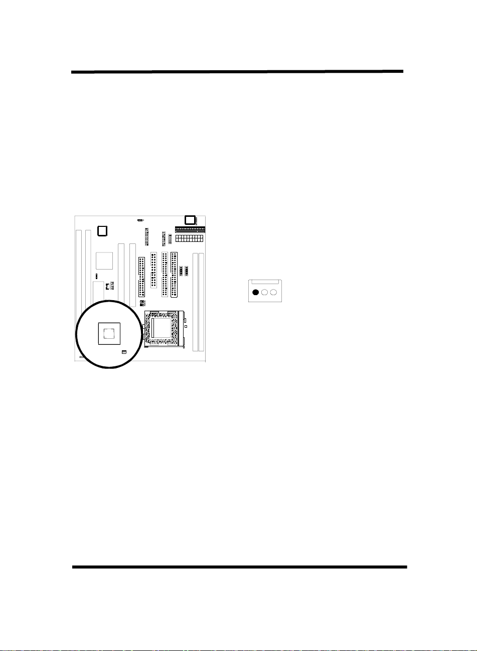
2-3-2 JP5: CMOS Status
JP5
is a 3-pin connector. Clear CMOS if system password is forgotten. Below is
details to show how to clear CMOS.
JP5
Pin1
JP5 CMOS Status
1-2 Normal
2-3 Clear CMOS
Procedure to clear CMOS:
Step 1: Shut down the system and disconnect the power supply from AC power.
Step 2: If the system uses ATX power, pull out the ATX cable from ATX connector.
Step 3: Short the CMOS jumper by putting jumper cap on Pin 2-3 for a few seconds.
Step 4: Return to pin 1-2 for normal setup.
Setp 5: Link power cable to the connector & connect AC power to power supply.
Step 6: Turn on system power.
if you’d like to set password, press “Del” Key during system bootup to enter
CMOS setup and establish a new password.
GXM Main Board 11
Page 17
5GXM
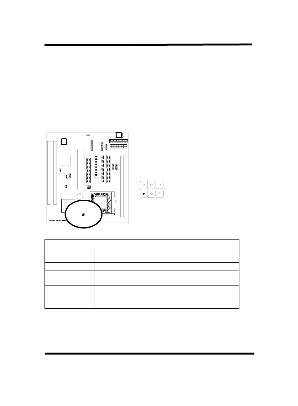
2-3-3 JP6: CPU Ratio Selector
JP6 is a 6-pin jumper to select CPU ratios.
JP6: CPU Ratio
2 4 6
1 3 5
JP6: CPU Ratio Selector
1-2 3-4 5-6
ON ON ON 4X
OFF OFF ON 5X
OFF ON OFF 6X
ON OFF OFF 7X
OFF OFF OFF 8X
ON OFF ON 9X
OFF ON ON 10X
GXM Main Board 12
CPU Ratio
Page 18

5GXM
2-4 Connectors
There are many connectors on this main board. Refer to the following pages for
details.
2-4-1 Front Panel Connectors
Front panel
“RESET,” “HD-LED,” “TBLED,” “ATX-SW.” Refer to details as below.
PW -L ED
has connectors as “POWER-LED,” “KEY LOCK,” “SPEAKER,”
Front Panel
K-LOCK
SPEAKER HDLED
RESET
ATX SW
TBLED
GXM Main Board 13
Page 19

5GXM
POWER LED
case front panel. The LED shows the status of the power.
KEYLOCK
front panel (if there is). Keyboard may be disconnected with the system
through this function.
Pin Operation
Open Normal
Close Short the connector to be disconnected with the system
SPEAKER connector
speaker to the main board for sound purpose.
RESET
on the case’s front panel. Shorting both pin 1& pin 2 can reset the system,
which is similar to the power off and then on again.
Pin Operation
Open Normal
Close Hardware reset
Marked “HDLED,”
strip. It is used to connect to front panel Hard Disk LED.
TBLED
status of system. It is used to connect to the Turbo Led on the front panel of the
case (if there is).
is a 3-pin connector. It is used to connect to the LED on the
is a 2-pin connector. It is used to connect the key lock on the case
is a 4-pin keyed Berg strip. It is used to connect to the case
is a 2 -pin keyed Berg strip, connected to the push button reset switch
Hard Disk activity LED connector is a 2-pin keyed Berg
with a 2-pin Berg strip on case front panel indicates the current speed
ATX SW
is ATX Soft-PWR with 2 pins.
GXM Main Board 14
Page 20

5GXM
2-4-2 Back Panel Connectors
There are COM1/ COM2, LPT1, USB1 and AT keyboard, PS/2 mouse on case
back panel. Please refer to more details as below.
COM1/COM2
The onboard serial port 1 and port 2
connector
setup. Please refer to Chapter 3 “Integrated Peripherals” for more information.
Pin Signal Pin Signal
Pin 1 Carrier detect (CD) Pin 5 Signal ground
Pin 2 Receive data (RXD) Pin 6 Data set ready
Pin 3 Transmit data (TX D) Pin 7 Request to send (RTS)
Pin 4 Data therminal ready (DTR) Pin 8 Clear to send (CTS)
Pin 9 Ring indicator Pin 10 None
COM1 and COM2.
COM1 and COM2 can be disabled in BIOS
are the 9-pin D-subminature male
COM2 COM1
GXM Main Board 15
Page 21

5GXM
LPT1
The onboard parallel port
Pin Signal Pin Signal
Pin 1 Strobe Pin 14 Auto feed
Pin 2 Data bit 0 Pin 15 Error
Pin 3 D ata bit 1 Pin 16 Init
Pin 4 D ata bit 2 Pin 17 SLCT in
Pin 5 Data bit 3 Pin 18 Ground
Pin 6 Data bit 4 Pin 19 Ground
Pin 7 Data bit 5 Pin 20 Ground
Pin 8 Data bit 6 Pin 21 Ground
Pin 9 Data bit 7 Pin 22 Ground
Pin 10 ACK Pin 23Ground
Pin 11 Busy Pin 24 Ground
Pin 12 PE Pin 25 Ground
Pin 13 SLCT Pin 26 None
is a 25-pin female connector, marked as
2 5 2 6
“LPT.”
LPT1
1 2
GXM Main Board 16
Page 22

5GXM
USB1 (Universal Serial Bus)
Universal Serial Bus connector
devices. There are 2 USB connectors on this main board.
, marked
Pin1
“USB1,”
USB1
is used to connect USB
AT Keyboard
AT KEYBOARD
GXM Main Board 17
Page 23

5GXM
PS/2 Mouse
PS/2 Mouse is a 5-pin connector to connect to mouse connector.
PS/2 MO U SE
1 M ouse CLK
2 M ouse data
3 None
4 GND
5 VCC
GXM Main Board 18
Page 24

5GXM
2-4-3 ATX Power Supply Connector
ATX power supply connector
especially. The ATX power supply supports the function of the
On Momentary switch”
SOFT-PWR
ATX power is turned on, the full power will not go into the system board until
the front panel switch is momentarily pressed. Push the switch again to turn off
the power to the system board.
Pin Signal Pin Signal
Pin 1 3 .3V Pin 2 3.3V
Pin 3 3.3V Pin 4 -12V
Pin 5 GND Pin 6 GND
Pin 7 5V Pin 8 SOFT-PWR ON
Pin 9 GND Pin 10 GND
Pin 11 5V Pin 12 GND
Pin 13 GND Pin 14 GND
Pin 15 RAWPOWER Pin 16 -5V
Pin 17 5V Pin 18 5V
Pin 19 +12V Pin 20 5V
on the system board
has 20 pins, which is designed for ATX case
“Soft Power
which connects on the front panel switch to the 2-pin
While the power switch on the back of
.
ATX POW ER
GXM Main Board 19
Page 25

5GXM
2-4-4 AT Power Supply Connector
AT P OW ER
Pin Signal Pin Signal
1 POWER GOOD 7 GROUND
2 +5V DC 8 GROUND
3 +12V DC 9 -5V DC
4 -12V 10 +5V DC
5 GROUND 11 +5V DC
6 GROUND 12 +5V DC
GXM Main Board 20
Page 26

5GXM
2-4-5 IR1 Connector
IR1 connector
application software like LAPlink, or WIN95 Direct Cable Connection, user
can transfer data to or from laptops, notebooks, PDA and printers. This
connector supports
Attach Infrared module to IR connector and enable BIOS “Infrared function.”
Be sure to put in the right orientation during attachment.
supports wireless infrared module. With this module and
HPSIR, ASKIR,
and
Fast IR
1 2
7 8
.
IR 1
GXM Main Board 21
Page 27
5GXM
2-4-6 FAN1 Connector
FAN1 connector has three pins.
FAN1
GROUND
+12V
SENSE
GXM Main Board 22
Page 28

5GXM
2-4-7 FDC1
FDC1 connector
with 34 pins is used to attach the floppy drive cable.
FDC1
1 2
3 3 3 4
Pin Signal Pin Signal
Pin 1 GND 2 Data rate selection
Pin 3 GND 4 NC
Pin 5 GND 6 NC
Pin 7 GND 8 FDC index
Pin 9 GND 10 FDD Motor A enable
Pin 11 GND 12 FDD Drive B enable
Pin 13 GND 14 FDD drive A enable
Pin 15 GND 16 FDD Motor enable
Pin 17 GND 18 FDC head direction
Pin 19 GND 20 FDC step pulse output to the drive during a SEEK operation
Pin 21 GND 22 FDC write enable serial data to the Drive
Pin 23 GND 24 FDC write enable identify
Pin 25 GND 26 Floppy disk track 0. Indicates that the head of the selected
Pin 27 GND 28 FDD write protect. Indicates that the disk of the selected
Pin 29 GND 30 Read disk data, serial data input input from the FDD
Pin 31 GND 32 Floppy disk side 1 select
Pin 33 GND 34 Floppy disk change. This is an input pin that senses whether
drive is on track zero.
drive is write-protected.
the drive door has been opened or a di skette has been
changed.
GXM Main Board 23
Page 29

5GXM
2-4-8 IDE 1 and IDE2
IDE 1/ IDE 2
both have 40 pins. There are 2 IDE connectors supported on this
system board. IDE1 is primary channel, and IDE2 is secondary channel. Each
channel supports 2 IDE devices, and 4 channels in total for this main board.
ID E1 ID E2
1 2 1 2
3 9 4 03 9 4 0
Pin Signal Pin Signal
Pin 1 IDE reset Pin 2 Ground
Pin 3 Data 7 Pin 4 Data 8
Pin 5 Data 6 Pin 6 Data 9
Pin 7 Data 5 Pin 8 Data 10
Pin 9 Data 4 Pin 10 Data 11
Pin 11 Data 3 Pin 12 Data 12
Pin 13 Data 2 Pin 14 Data 13
Pin 15 Data 1 Pin 16 Data 14
Pin 17 Data 0 Pin 18 Data 15
Pin 19 Ground Pin 20 Key (NC)
Pin 21 PDREQ Pin 22 Ground
Pin 23 I/O write Pin 24 Ground
Pin 25 I/O read Pin 26 Ground
Pin 27 NC Pin 28 ALE
Pin 29 NC Pin 30 Ground
Pin 31 IDE IRQ 14 Pin 32 IOSC15
Pin 33 Address A1 Pin 34 NC
Pin 35 Address A0 Pin 36 Address A2
Pin 37 IDE chip select 0 Pin 38 IDE chip select 1
Pin 39 IDE active Pin 40 Ground
GXM Main Board 24
Page 30

5GXM
2-4-9 J1: CD-IN
J1 is a 4-pin CD-in co nnecttor.
J1: CD-IN
2-4-10 J2: Multi-media Connector
J2 is a 20-pin connector. It is connected to the enclosed 20-pin cable to provid
multi-media functions like VGA, MIC, LINE-IN, LINE-OUT, TV-OUT and SVIDEO functions.
GXM Main Board 25
Page 31

5GXM
J2: M u lti-m e dia Conn e cto r
2 1
2 0 1 9
Below is 20-pin multi-media module connecting to the above 20-pin J2
connector.
FOR 20-PIN J2 connector
VGA1 MIC
LINE-IN
LINE-OUT
TV-OUT
S-VIDEO
GXM Main Board 26
Page 32

5GXM
2-4-11 J3: Wake Up On LAN
Wake up on LAN,
marked as
is a 3-pin connector. To support this
“J3,”
feature, a network card is required for the system and a network management
software must be installed too.
J3: Wake Up On LAN
1 5V trickle voltage
2 GND
3. PM E signal
Wake up on LAN function requirement:
Power should offer at least 750mA to the signal “5V trickle voltage” to support
WOL function
GXM Main Board 27
Page 33

5GXM
2-4-12 Game Port
Game port is a 16- pin connector connecting to joystick cable.
GAME PORT
1 2
1 5 16
GXM Main Board 28
Page 34

5GXM
2-5 DIMM Memory Installation
has 2 DIMMs on board and memory interface is directly from CPU. Only
5GXM
SDRAM memory is supported. Either DIMM 1, DIMM2 supports 8 MB, 16 MB,
32 MB, 64 MB, and 128MB. Maximum memory for SDRAM is up to 256 MB.
Insert the module as shown. Due to different number of pins on either side of the
breaks, the module will only fit in the orientation as shown.
DIMM
Chipset only supports SDARAM memory, and does not support EDO RAM
memory.
GXM Main Board 29
Page 35

5GXM
Chapter 3 BIOS Setup
3-1 Award BIOS CMOS Setup
The menu displays all the major selection items and allow user to select any of
shown item. The selection is made by moving cursor (press any direction key ) to
the item and press <Enter> key. An on-line help message is displayed at the
bottom of the screen as cursor is moving to various items which provides user
better understanding of each function. When a selection is made, the menu of
selected item will appear. So the user can modify associated configuration
parameters.
GXM Main Board 30
Page 36

5GXM
3-2 Standard CMOS Setup
The
”Standard CMOS Setup”
current date
drive type,
BIOS and displayed for your reference. When a field is highlighted (direction keys
to move cursor and
by pressing
from the keyboard.
and
time, type of hard disk drive
and the type of
<Enter>
<PageDown>
allows user to configure system setting such as
installed in the system,
display monitor.
key to select). The entries in the field will be changed
or
<PageUp>
Memory size is auto detected by the
key or user can enter new data directly
floppy
GXM Main Board 31
Page 37

5GXM
Hard Disk Configurations
1. TYPE
: select from
of disk drives. Select
"AUTO"
2. SIZE :
3. CYLS :
4. HEAD :
the hard disk size. The unit is mega byte(MB).
the cylinder number of the hard disk.
the read/write head number of hard disk. The range is from
"16".
5. PRECOMP
6. LANDZ
: the cylinder number that the disk drive heads (read/write) are seated
when the disk drive is parked.
7. SECTOR
is from
8. MODE
:select
disk supports the
However, if your hard disk cyclinder is more than 1024 and does not
support the lba function, you have to set at
"NORMAL"
Note 1:
“auto,”
Note2: "halt on"
during POST.
"1" to "45"
to fill remaining fields with redefined values
"USER"
to fill the remaining fields. Select
to detect the HDD type automatically.
"1" to
: the cylinder number at which the disk drive changes the write
timing.
: the sector number of each track defined on the hard disk. The range
"1"
"64".
to
"AUTO"
to detect the mode type automatically. If your hard
LBA
mode, select
"LBA"
"LARGE.”
or
"LARGE".
Select
if your hard disk supporting cylinder is below 1024.
if hard disk primary master/slave and secondary master/slave were set to
the hard disk size and model will be auto detected on display during POST.
is to determine when to halt the system by the BIOS if error occurs
GXM Main Board 32
Page 38

5GXM
3-3 BIOS Features Setup
Menu below shows all of the manufacturer's default values of this main board.
Move the cursor by pressing direction keys and
to modify the parameters, pressing
selected item. This setup program also provide 2 convenient ways to load the
default parameter data from BIOS
corrupted. This provides the system a capability to recover from any possible
error.
[F1]
[F6]
<PageDown>
key to display help message of the
or CMOS
[F7]
or
<PageUp>
area if shown data is
key
Anti-Virus Protection
:Enabled
:Disabled
CPU Internal Cache
Enabled
Disabled:
(default)
(default): enable L1 cache
disable L1 cache
GXM Main Board 33
Page 39

5GXM
Quick Power On Self Test
This category speeds up power on self test.
Enabled :
Disabled:
Boot sequence
This category determines which drive the system searches first. Take
for example. System will search in turn for floppy disk drive; second is hard disk
drive, and finally SCSI drive. Default value is
below:
A,C,SCSI; C,A,SCCI; C,CDROM,A; CDROM,C,A; D,A,SCSI; E,A,SCSI;
F,A,SCSI; SCSI,A,C; SCSI,C,A; C Only; LS/ZIP,C.
Swap Floppy Drive
Enabled:
Disabled
Boot Up Floppy Seek
BIOS will determine if the floppy disk drive is 40 or 80 tracks. 360k type is 40
tracks while 720K/ 1.2M and 1.44M are all 80 tracks. Default value is
“Disabled.”
BIOS will shorten or skip some check items.
normal speed
“A,C,SCSI.”.
floppy A&B will be swapped.
(default): floppy A&B will be not swapped.
“A,C,SCSI”
Options are as
Boot Up Numlock Status
:On
(default)
:Off
Gate A20 Option
:Normal
:Fast
(default)
GXM Main Board 34
Page 40

5GXM
Memory Parity Check
This item allows memory parity check function.
:Enabled
:Disabled
Typematic Rate Setting
This determines the typematic rate.
Enabled:
Disabled
system bios will use default value of this 2 items and the default is controlled by
keyboard.
Typematic Rate(Chars/Sec)
6: 6 Characters Per Second(default)
8: 8 Characters Per Second
10 : 10 Characters Per Second
12: 12 Characters Per Second
15: 15 Characters Per Second
20: 20 Characters Per Second
24: 24 Characters Per Second
30 : 30 Characters Per Second
(default)
enable typematic rate and typematic delay programming.
(default): disable typematic rate and typematic delay programming. The
Typematic Delay (Msec)
This is the interval between the first and second character displayed.
250 :
250 msec (default)
500 :
500 msec
750 :
750 msec
1000 :
1000 msec
Security Option
:Setup
Setting password in BIOS CMOS
the user needs to key in password if entering BIOS CMOS setup.
:System
This function secures the system under system boot-up and BIOS setup.
(default)--- security protecti on in CMOS setup menu
“Supervisor Password” or User Password,
---security protection in system boot-up & BIOS setup
GXM Main Board 35
”
Page 41

5GXM
PCI/VGA Palette Snoop
Enabled:
Disabled (default):
snoop function, please set at
OS Select For DRAM> 64MB
This option is especially set for OS2 operating system. Set
memory over 64MB and set
Windows® 95/98 or Windows NT.
:Non-OS2 (default)
:OS2
Video BIOS Shadow
It determines whether video BIOS will be copied to RAM. However, it is optional
from chipset design. Video shadow will increase the video speed.
Enabled :
Disabled:
C8000-CBFFF Shadow, CC000-CFFF Shadow, D0000-D3FFF Shadow:
D4000-D7FFF Shadow, D8000-DBFFF Shadow, DC000-DFFF Shadow
These are categories determining whether optional ROM will be copied to RAM
by 16KB or 32KB per unit and the size depends on chipset.
:Enabled
:Disabled
it allows you to install an enhanced graphics adapter card.
If your graphics adapter card does not support the pallette
Disabled
Video Shadow is enabled (default)
Video Shadow is disabled
(default)
to avoid system malfunction.
“Non-OS2”
for other operating systems like
“OS2”
for RAM
GXM Main Board 36
Page 42

3-4 Chipset Features Setup
5GXM
SDRAM CAS Cycle Length:
leadoff timing.
:2 T
(default)
:3 T
USB Controller
:Enabled
Enabling this function adds the function of
:Disabled
USB Legacy Support
:Disabled
:Enabled---
(default)
(default)
enable USB keyboard or USB mouse
control the DRAM page missing and row miss
GXM Main Board 37
“USB Legacy Support.”
Page 43

3-5 Power Management Setup
IRQ1 (KeyBoard) : ON
IRQ3 (COM2) : OFF
IRQ4 (COM1) : OFF
IRQ5 (LPT2) : OFF
IRQ6 (Floppy Disk) : OFF
IRQ9 (IRQ2 Redir) : OFF
IRQ10 (Reserved) : OFF
IRQ11 (Reserved) : OFF
IRQ12 (PS/2 Mouse) : OFF
IRQ13 (Coprocessor) : OFF
Disabled
IRQ14 (Hard Disk) : OFF
IRQ15 (Reserved) : OFF
5GXM
Power Management
:User Define
(default)--users can configure their own power management
:Min Saving
:Max Saving
:Disabled
** PM Timers **
HDD Power Down
:Disabled
(default)
:1/2/3/4/5/6/8/10/2/15/16/20/30/40/60 min.
Doze Mode
:Disabled (default)
:1/2/4/8/10/12/16 SEC
GXM Main Board 38
Page 44

Net POWER ON Controller (Wake up on LAN function)
:Enabled
:Disable
(default)
To support functions such as “Wake up on LAN,” “Keyboard Wake up,” or “PS/2
Mouse Wake up,” we suggest that Pin 17 signal 5VSB on ATX Power supply should
be able to offer at least 750 mA driving ability.
RING POWER ON CONTROLLER
:Disabled
:Enabled:
(default)
modem ring on function--- system ca n be turned on through modem.
Note: this function only works when the system is turned off from Windows mode, and
Doze mode will not function.
5GXM
RTC Alarm function:
Enabled:
Disable
key in the time of the day. System will turn on then.
(default) : disble this function.
Note: this function only works when the system is turned off in Windows mode, and
doze mode will not function.
auto power on at the appointed time.
GXM Main Board 39
Page 45

3-6 PNP / PCI Configuration Setup
5GXM
PNP OS Installed
(default)
:No
OS will not recognize PnP devices.
:Yes
OS will arrange the setup of PnP devices.
Resources Controlled By
:Manual
The table will show the below items:
assigned to, DMA-0 assigned to.”
required.
:Auto
The table will not show the above items, and the system will automatically assign
the above setup.
(default)
“Reset Configuration Data, IRQ-3
The user can adjust the shown items as
GXM Main Board 40
Page 46

5GXM
Reset Configuration Data
:Disabled
:Enabled---
exit setup if you have installed a new add-on card and the system reconfiguration
has caused such a serious conflict that the operating system can not boot up.
IRQ-3 Assigned To---- IRQ-15 Assigned To
: PCI/ISA PnP
: Legacy ISA
DMA-0 Assigned To--- DMA-7 Assigned To
: PCI/ISA PnP
: Legancy ISA
PCI IRQ Actived By
There are 2 modes in activating PCI IRQ.
:Edge
:Level
(default)
to reset
(default)
“Extended System Configuration Data(ESCD)
(default)
(default)
when yo u
GXM Main Board 41
Page 47

3-7 Integrated Peripherals
2F8/IRQ3
378/IRQ7
SPP
5GXM
IDE HDD Block Mode
: Enabled
(default)
: Disabled
Primary IDE Channel
: Enabled
(default)--- it allows to adjust the items
and Slave Drive PIO Mode.”
: Disabled
Secondary IDE Channel
:Enabled
(default)--- it allo ws to a djust the items
Slave Drive PIO Mode.”
: Disabled
GXM Main Board 42
“Master Drive PIO Mode,
“Master Drive PIO Mode, and
Page 48

Onboard FDC Controller
: Enabled
: Disabled
Onboard Serial Port 1
: 3F8/IRQ4
: 2F8/IRQ3
: 3E8/IRQ4
: 2E8/IRQ3
: Auto
: Disabled
Onboard Serial Port 2
: 3F8/IRQ4
: 2F8/IRQ3
: 3E8/IRQ4
: 2E8/IRQ3
: Auto
: Disabled
(default)
(default)
(default)
5GXM
UR2 Mode
: Standard
: Sharp IR
: IrDA SIR
Onboard Parallel Port
: 378/IRQ7
: 3BC/IRQ7
: 278H/IRQ5
: Disabled
(default)
(default)
GXM Main Board 43
Page 49

Parallel Port Mode
SPP
(Default)
EPP
ECP
ECP+EPP
Build in CPU Audio
This function is to enable the built-in CPU audio function.
: Enable (default)
: Disable
Audio I/O Base Address
:220H
(default)
:240H
:260H
:280H
Choosing this item, there is another line shown:
ECP Mode Use DMA: 3
Choosing this item, another line is shown:
ECP Mode Use DMA: 3
(default)
(default)
/ 1
/ 1
5GXM
MPU-401 I/O Base Address
:330H
(deafult)
:Disable
Audio IRQ Select
This function is to select the IRQ.
: IRQ 5
: IRQ 3
: IRQ 10
: Disable
Audio Low DMA Select
: DMA 0
: DMA 1
: Disable
(deafult)
(default)
GXM Main Board 44
Page 50

Audio High DMA Select
: DMA 5
: DMA 6
: DMA 7
: Disable
Joystick Status
This function allows the use of joystick.
: Enabled
: Disabled
Multiple Monitor Support
The system will decide which VGA function is detected first.
: M/B first (default)
: PCI first
: No onboard
Video Memory Size
This will decide the Video Memory size sharing from the system memory.
: 4.0 M
: 1.5 M
: 2.5 M
(default)
(default)
(default)
5GXM
TV output Mode
: NTSC
: PAL
(default)
GXM Main Board 45
Page 51

3-8 Supervisor/User Password
5GXM
The
"Supervisor/User Password setting"
There are two kinds of password functions in the setup menu : one is “
Password
Supervisor Password
of setup menu.
User Password
to change the options of the setup menu except “
& EXIT SETUP,”
1. How to set “Supervisor Password” & “User Password”
The setup of
steps.
Step 1:
Press
,” and the other is
: this function only allows you to enter the setup menu but not
and
“Supervisor Password”
Enter Password
<Enter>
after appointing the password.
“User Password.”
: this function allows you the right to change the options
“EXIT WITHOUT SAVING.”
utility sets the security protection.
Their difference is
and
“User Password”
USER PASSWORD,” “SAVE
:
have the same
Supervisor
ENTER PASSWORD:
GXM Main Board 46
Page 52

5GXM
Step 2:
Typing the password again and pressing
Step 3: Set
Confirm Password
CONFIRM PASSWORD:
Note:
If you forget password, please clear CMOS.
(refer to jumper JP5 CMOS status )
“Security Option” in “BIOS Features Setup”
<Enter>
.
After setting password, enter
There are 2 options
“System”
CMOS setup..
secures PC sytem and password is required during system boot- up and
“Setup” & “System.” “Setup”
“Security Option” in “BIOS Features Setup.”
GXM Main Board 47
secures CMOS setup.
Page 53

2. How to Disable “Supervisor Password” & “User Password”
5GXM
Step 1:
Setp 2:
After enter, it shows “Enter Password.” Press the
entering a new password when
“PASSWORD DISABLED PRESS ANY KEY TO CONTINUNE.”
key as instructed to disable password.
Go to CMOS Setup Menu
Enter “Supervisor Password” or “User Password”
PASSWORD DISABLED!!!
PRESS ANY KEY TO CONTINUE…
(need to key in password first)
"ENTER PASSWORD"
<Enter>
appears. It will inform
key instead of
Pess any
GXM Main Board 48
Page 54

3-9 IDE HDD Auto Detection
HARD DISK TYPE SIZE CYLS HEAD PRECOMP LANDZ SECTOR MODE
Primary Master:
Primary Slave:
Secondary Master:
Secondary Slave:
Select Primary Master Option (N: Skip): N
OPTIONS SIZE CYLS HEAD PRECOMP LANDZ SECTOR MODE
2 (Y) 4302 523 255 0 8893 63 LBA
1 4303 8894 15 65535 8893 63 NORMAL
3 429 6555 2405 65535 8893 63 LARGE
Note: Some OSes (like SCO-UNIX) must use “NORMAL” for installation.
5GXM
The
"IDE HDD AUTO DETECTION"
utility is a very useful tool especially
when you do not know which kind of hard disk type you a re using. You can use
this utility to detect the correct disk type installed in the system automatically or
you can set hard disk type to auto in the standard CMOS setup. You don't need the
"IDE HDD Aauto Detection"
utility. The BIOS will auto-detect the hard disk
size and model on display during post.
GXM Main Board 49
Page 55

5GXM
The Award® BIOS supports 3 HDD modes:
1. Normal mode
Generic access mode in which neither the BIOS nor the IDE controller will make
any transformations during accessing.
The maximum number of cylinders, head & sectors for normal mode are
& 63.
No. Cylinder (1024)
X No. Head (16)
X No. Sector (63)
X No. Per Sector (512)
528 MB
If user set this HDD to normal mode, the maximum accessible HDD size will b e
528 MB even though its physical size may be greater than that!
2. LBA (Logical Block Addressing) Mode
A new HDD accessing method to overcome the 528 MB bottleneck. The number
of cylinders, heads & sectors shown in setup may not be the number physically
contained in the HDD. During HDD accessing, the ide controller will transform
the logical address described by sector, head & cylinder into its own physical
address inside the HDD.
NORMAL, LBA & LARGE.
1024, 16
The maximum HDD size supported by LBA mode is 8.4 GB which is obtained by
the following formula:
No. Cylinder (1024)
X No. Head (255)
X No. Sector (63)
X No. Bytes Per Sector (512)
8.4 GB
GXM Main Board 50
Page 56

5GXM
3. Large Mode
Extended HDD access mode supported by Award® software. Some IDE HDDs
contain more than 1024 cylinder without LBA support (in some cases, user do not
want LBA). The Award® BIOS provides another alternative to support these
kinds of large mode:
Cyls. Head Sector Mode
1120 16 59 NORMAL
560 32 59 LARGE
BIOS tricks DOS (or other OS) that the number of cylinders is less than 1024 by
dividing it by 2. At the same time, the number of heads is multiplied by 2. A
reverse transformation process will be made inside int 12h in order to access the
right HDD address the right HDD address!
4. Maximum HDD Size:
No. Cylinder (1024)
X No. Head (32)
X No. Sector (63)
X No. Bytes Per Sector (512)
1 GB
To support LBA or large mode of HDDs,
softwares involved. All these softwares are located in the Award®
HDD service routine (int 13h). It may be failed to access a HDD with LBA
(large) mode selected if you are running under an perating system which
replaces the whole int 13h. Unix operating systems do not support either LBA or
large and must utility the standard mode. Unix can support drives larger than
528MB.
there must be some
GXM Main Board 51
Page 57

3-10 Load Setup Defaults
5GXM
"Load Setup Defaults"
ROM. The auto-configured settings only affect “
“Chipset Features Setup”
setup. To use this feature, highlight it on the main screen and press the
key. A line will appear on screen asking if you want to load the setup default
values. Press the
will then load. Press
<Y>
loads optimized settings which are stored in the BIOS
BIOS Features Setup”
screens. There is no effect on the standard CMOS
key and then press the
if you don't want to
<N>
<Enter>
key . The setup defaults
and
<Enter>
GXM Main Board 52
Page 58

3-11 Save & Exit Setup
5GXM
The
"Save & Exit Setup"
all the changes, you have made which are recorded in the CMOS RAM.
option will bring you back to boot up procedure with
GXM Main Board 53
Page 59

3-12 Quit Without Saving
5GXM
The
"Quit Without Saving"
procedure without saving any data into CMOS RAM. All of the old data in the
CMOS will not be destroyed.
option will bring you back to normal boot up
GXM Main Board 54
Page 60

Chapter 4 Appendix
4-1 Memory Map
Address range Size Description
00000-7FFFF 512K Conventional memory
80000-9FBFF 127K Extended conventional memory
9FC00-9FFFF 1K Extended BIOS data area if PS/2 mouse is
installed
A0000-C7FFF 160K Available for hi DOS memory
C8000-DFFFF 96K Available for hi DOS memo ry and adapter
ROMs
E0000-EEFFF 60K Available for UMB
EF000-EFFFF 4K Video service routine for monochrome &
CGA adapter
F0000-F7FFF 32K BIOS CMOS setup utility
F8000-FCFFF 20K BIOS runtime service routine (2)
FD000-FDFFF 4K Plug and play escd data area
FE000-FFFFF 8K BIOS runtime service routine (1)
5GXM
GXM Main Board 55
Page 61

4-2 I/O Map
000-01F DMA controller (master)
020-021 Interrupt controller (master)
022-023 Chipset control registers. I/o posts
040-05F Timer control registers
060-06F Keyboard interface controller (8042)
070-07F RTC ports & CMOS I/O ports
080-09F DMA register
0A0-0BF Interrupt controller (slave)
0C0-0DF DMA controller (slave)
0F0-0FF Math coprocessor
1F0-1FB Hard disk controller
278-27F Parallel port 2
2B0-2DF Graphics adapter controller
2F8-2FF Serial port 2
360-36F Network ports
378-37F Parallel port 1
3B0-3BF Monochrome & parallel port adapter
3C0-3CF EGA adapter
3D0-CDF CGA adapter
3F0-3F7 Floppy disk controller
3F8-3FF Serial port-1
5GXM
GXM Main Board 56
Page 62

4-3 Time & DMA Channels Map
Time map:
Timer channel 1 DRAM refresh request
Timer channel 2 speaker tone generator
Timer channel 0 system timer interrupt
5GXM
Dma channels:
DMA channel 1 onboard ecp (option)
DMA channel 2 floppy disk (smc chip)
DMA channel 3 onboard ECP (default)
DMA channel 4 cascade for dma controller 1
DMA channel 5 available
DMA channel 6 available
DMA channel 7 available
DMA channel 0 available
GXM Main Board 57
Page 63

4-4 Interrupt Map
5GXM
NIMI:
IRQ(H/W):
0 system timer interrupt from timer 0
1 keyboard output buffer full
2 cascade for IRQ 8-15
3 serial port2
4 serial port1
5 parallel port 2
6 floppy disk (smc chip)
7 parallel port 1
8 RTC clock
9 available
10 available
11 available
12 PS/2 mouse
13 math coprocessor
14 onboard hard disk (ide1) channel
15 onboard hard disk (ide2) channel
non-maskable interrupt
GXM Main Board 58
Page 64

4-5 RTC & CMOS RAM Map
RTC & CMOS :
00 seconds
01 second alarm
02 minutes
03 minutes alarm
04 hours
05 hours alarm
06 day of week
07 day of month
08 month
09 year
0a status register a
0b status register b
0c status register c
0d status register d
0e diagnostic status byte
0f shutdown byte
10 floppy disk drive type byte
12 hard disk type byte
13 reserve
14 equipment type
15 base memory low byte
16 base memory high byte
17 extension memory low byte
18 extension memory high byte
19-2d
2e-2f
30 Reserved for extension memory low byte
31 reserved for extension memory high byte
32 date century byte
33 information flag
34-3f reserve
40-7f reserved for chipset setting data
5GXM
GXM Main Board 59
Page 65

4-6 Award BIOS Hard Disk Type
5GXM
Type Cylinder Heads Write
Pre-comp
1 306 4 128 305 17 10MB
2 615 4 300 615 17 21MB
3 615 6 300 615 17 32MB
4 940 8 512 940 17 65MB
5 940 6 512 940 17 49MB
6 615 4 65535 615 17 21MB
7 462 8 256 511 17 32MB
8 733 5 65535 733 17 31MB
9 900 15 65535 901 17 117MB
10 820 3 65535 820 17 21MB
11 855 5 65535 855 17 37MB
12 855 7 65535 855 17 52MB
13 306 8 128 319 17 21MB
14 733 7 65535 733 17 44MB
16 612 4 0 663 17 21MB
17 977 5 300 977 17 42MB
18 977 7 65535 977 17 59MB
19 1024 7 512 1023 17 62MB
20 733 5 300 732 17 31MB
21 733 7 300 732 17 44MB
22 733 5 300 733 17 31MB
23 306 4 0 336 17 10MB
24 977 5 0 925 17 42MB
25 1024 9 65535 925 17 80MB
26 1224 7 65535 754 17 74MB
27 1224 11 65535 754 17 117MB
28 1224 15 65535 699 17 159MB
29 1024 8 65535 823 17 71MB
30 1024 11 65535 1023 17 98MB
Landing
Zone
Sectors Size
GXM Main Board 60
Page 66

5GXM
Type Cylinder Heads Write
Pre-comp
31 918 11 65535 1023 17 87MB
32 925 9 65535 926 17 72MB
33 1024 10 65535 1023 17 89MB
34 1024 12 65535 1023 17 106MB
35 1024 13 65535 1023 17 115MB
36 1024 14 65535 1023 17 124MB
37 1024 2 65535 1023 17 17MB
38 1024 16 65535 1023 17 142MB
39 918 15 65535 1023 17 119MB
40 820 6 65535 820 17 42MB
41 1024 5 65535 1023 17 44MB
42 1024 8 65535 1023 17 68MB
43 809 6 65535 852 17 42MB
44 809 9 65535 852 17 64MB
45 776 8 65535 775 17 104MB
46 AUTO 0 0 0 0
47 USER’S TYPE
Landing
Zone
Sectors Size
GXM Main Board 61
Page 67

4-7 ISA I/O Address Map
5GXM
I/O Address
000 - 01F DMA Controller 1, 8237A-5
020 - 03F Interrupt Controller 1, 8259A
040 - 05F System Timer, 8254-2
060 - 06F 8742 Keyboard Controller
070 - 07F real-time Clock/CMOS and NMI Mask
080 - 09F DMA Page Register, 74LS612
0A0 - 0BF Interrupt Controller 2, 8259A
0C0 - 0DF DMA Controller 2, 8237A-5
0F0 - 0FF i486 Math Coprocessor
1F0 - 1F8 Fixed Disk Drive Adapter
200 - 207 Game I/O
20C - 20D Reserved
278 - 27F Parallel Printer Port 2
2B0 - 2DF Alternate Enhanced Graphic Adapter
2E2 - 2E3 Data Acquisition Adapter 0
2F8 - 2FF Serial Port 2 (RS-232-C)
300 - 31F Prototype Card
360 - 363 PC Network (Low Address)
364 - 367 Reserved
368 - 36B PC Network (High Address)
36C - 36F Reserved
378 - 37F Parallel Printer Port 1
380 - 38F SDLC, Bisynchronous 2
390 - 393 Cluster
3A0 - 3AF Bisynchronous 1
3B0 - 3BF Monochrome Display and Printer Adapter
(HEX)
21F Reserved
2E1 GPIB Adapter 0
I/O device
GXM Main Board 62
Page 68

5GXM
I/O Address
3C0 - 3CF Enhanced Graphics Adapter
3D0 - 3DF Color/Graphics Monitor Adapter
3F0 - 3F7 Diskette Drive Controller
3F8 - 3FF Serial Port 1 (RS-232-C)
6E2 - 6E3 Data Acquisition Adapter 1
790 - 793 Cluster Adapter 1
AE2 - AE3 Data Acquisition Adapter 2
B90 - B93 Cluster Adapter 2
EE2 - EE3 Data Acquisition Adapter 3
1390 - 1393 Cluster Adapter 3
2390 - 2393 Cluster Adapter 4
(HEX)
22E1 GPIB Adapter 1
42E1 GPIB Adapter 2
62E1 GPIB Adapter 3
82E1 GPIB Adapter 4
A2E1 GPIB Adapter 5
C2E1 GPIB Adapter 6
E2E1 GPIB Adapter 7
I/O device
GXM Main Board 63
Page 69

5GXM
Chapter 5 Q & A
5-1 Errors Messages During Power On Self Test
During power on self test (post), BIOS will automatically detect the system
devices. Below is the questions that users may always meet. The user may press
“Esc” key to skip the full memory test.
Beep sound
1.
On power on, the system make beep sound to offer different messages. If the
system is configured correctly, it prompts a short beep to show correct the
devices configuration is done correctly. When VGA card and DIMM modules
are not plugged well, the system makes longer and constant beep sound s.
BIOS ROM checksum error
2.
It indicates the checksum of the BIOS code is not right and system will always
halt on power on screen. Contact the dealer to exchange a new BIOS.
CMOS battery fails
3.
It indicates the CMOS battery does not work. Contact the dealer to exchange
a new BIOS.
CMOS checksum error
4.
It indicates the CMOS checksum is incorrect. Load the default values in
BIOS to solve this problem. This error may result from a weak BIOS, so
exchange a new BIOS if necessary.
Hard disk initialize
5.
Please wait a moment…
Some hard drives require more time to initialize.
GXM Main Board 64
Page 70

6. Hard disk install failure
The system can not find or initialize the hard drive controller or the drive.
Check if the controller is set correctly. If no hard disk is installed,
drive selection”
Keyboard error or no keyboard present
7.
This means the system can not initialize the keyboard. Check if the keyboard
is plugged well and be sure no keys are pressed during POST.
Keyboard is lock out- Unlock the key
8.
Normally when this message comes out, check if there is anything mis-placed
on the keyboard. Be sure nothing touches the keys.
Memory test fails
9.
There will be more information to specify the type and location of the memory
error.
Primary master hard disk fail
10.
The BIOS find an error in the primary master hard disk drive.
must be set to
“none.”
“Hard
5GXM
11.
Primary slave hard disk fail
The BIOS finds an error in the primary slave hard disk drive.
12.
Secondary master hard disk fail
The BIOS finds an error in the secondary slave master hard disk drive.
13.
Secondary slave hard disk fail
The BIOS finds an error in the secondary slave IDE hard disk drive.
GXM Main Board 65
Page 71

5GXM
5-2 Web-site Service
If you have any questions this manual may not help, like up dated BIOS, or any
information you need regarding our products, please visit our web-site at
http://www.lucky-star.com.tw
Website to bundle updated “XStore Pro” IDE driver
Updated drivers will be constantly provided at High Point’s website. Luck Star
website is also linked to High Point.
http://highpoint-tech.com
GXM Main Board 66
 Loading...