


Advisory
August 5, 1999
TMPR28051 STS-1/AU-3 (STM-0) Mapper
Device Advisory for Version 5 of the Device
Register Architecture (RA) Map
RA-1. Reset Bit
The software reset bit (bit 0) of register 0x00 is not functional.
RA-2. Transmit Path AIS Insert Bit
The TXPAISINS bit (bit 5) of register 0x01 produces both AIS-P and AIS-L.
RA-3. STS-1 Loss of Pointer Mask Bit
The STS1LOPMSK bit (bit 2) of register 0x04 masks both STS1LOP and STS1LOF.
RA-4. STS-1 Loss of Frame Mask Bit
The STS1LOFMSK bit (bit 1) of register 0x04 is not functional.
RA-5. VTLABCOM and VTRFIRDICOM Interrupt Bits
Occasionally, it might require multiple reads to clear the composite interrupt bits VTLABCOM (bit 2 of
register 0x05) and VTRFIRDICOM (bit 4 of register 0x05).
Error Insertion (EI)
EI-1. DS1/E1 Alarm Indication Signal
The device does not insert DS1/E1 AIS towards the STS-1 if there is an LOC condition in the incoming DS1/E1
signal.
EI-2. LOC Condition in E1 Loopback Mode
In the absence of an input clock, the device detects an LOC condition and generates TU-AIS upstream, even if the
loopback path is selected (the loopback signal is overwritten by TU-AIS).

TMPR28051 STS-1/AU-3 (STM-0) Mapper Advisor
y
(
)
)
(
q
(
g
(
)
g
)
(
)
Device Advisory for Version 5 of the Device August 5, 1999
Error Insertion (EI)
continued
EI-3. False S-BIP, L-BIP, and P-BIP Error Insertion
The device transmits S-BIP, L-BIP, and P-BIP errors when configured for automatic insertion of REI, and certain
STS-1 error conditions such as LOS, LOF, LOP-P, S-BIP, L-BIP, and P-BIP are inserted.
VT Alarms (VT
VT-1. VT Path Payload Label Mismatch
The device reports PLM-V when it detects three consecutive consistent new values for the VT label. This is in compliance with G.783 Section 2.2.2.7 and T1.231 Section 8.1.3.5.2.4.2 specifications, but is not compliant with
GR-253 Section 6.2.1.1.8.C.
VT-2. Failure in the Detection of VT Loss of Pointer Defects
The device also apparently fails to detect an LOP-V defect when it continuously receives a VT pointer word of
6C68
i.e., a value indicating a VT1.5 with an offset of 104 bytes, versus a maximum valid offset of 103 bytes). In
this case, the device inserts the re
nonconformance to GR 253, R6-71).
ure
uired DS1 AIS downstream, but does not subsequently declare an LOP-V fail-
VT-3. Inappropriate Termination of VT Loss of Pointer Defect Condition
After the device has detected an LOP-V defect, it inappropriately terminates that defect upon receiving two pointer
words containin
terminated unless a valid pointer is received in three consecutive VT superframes
R6-75
.
the same value as the previous valid pointer. According to GR 253, an LOP-V defect must not be
nonconformance to GR 253,
VT-4. Inappropriate Termination of VT Alarm Indication Signal Defect Condition
After the device has detected an AIS-V defect, it inappropriately terminates that defect upon receiving two pointer
words containin
0110
. According to GR 253, an AIS-V defect must not be terminated unless a normal valid pointer is received in
three consecutive VT superframes, or a valid pointer with a set NDF is received in one VT superframe
mance to GR 253, R6-183
For additional information, contact your Microelectronics Group Account Manager or the following:
INTERNET:
E-MAIL:
N. AMERICA: Microelectronics Group, Lucent Technologies Inc., 555 Union Boulevard, Room 30L-15P-BA, Allentown, PA 18103
ASIA PACIFIC: Microelectronics Group, Lucent Technologies Singapore Pte. Ltd., 77 Science Park Drive, #03-18 Cintech III, Singapore 118256
CHINA: Microelectr on ic s G r ou p, Lucent Techno lo gies (China) Co. , Ltd., A-F2, 23/F, Zao Fon g U niverse Building, 1800 Zhong Shan Xi Road, Shanghai
JAPAN: Microelectronics Group, Lucent Technologies Japan Ltd., 7-18, Higashi-Gotanda 2-chome, Shinagawa-ku, Tokyo 141, Japan
EUROPE: Data Requests: MICROELECTRONICS GROUP DATALINE:
Lucent Technologies Inc. reserves the right to make changes to the product(s) or information contained herein without notice. No liability is assumed as a result of their use or application. No
rights under any patent accompany the sale of any such product(s) or information.
the same value as the previous valid pointer and without a set NDF (e.g., with the N bits set to
.
http://www.lucent.com/micro
docmaster@micro.lucent.com
1-800-372-2447
Tel. (65) 778 8833
200233 P. R. China
Tel. (81) 3 5421 1600
Technical Inquiries: GERMANY:
, FAX 610-712-4106 (In CANADA:
, FAX (65) 777 7495
Tel . ( 86) 21 6440 0468, ext. 316
, FAX (81) 3 5421 1700
FRANCE:
(39) 02 6608131
ITALY:
(49) 89 95086 0
(33) 1 40 83 68 00
1-800-553-2448
, F A X ( 86) 21 6440 0652
(Munich), UNITED KINGDOM:
(Paris), SWEDEN:
(Milan), SPAIN:
, FAX 610-712-4106)
Tel. (44) 7000 582 368
(34) 1 807 1441
, FAX (44) 1189 328 148
(44) 1344 865 900
(46) 8 594 607 00
(Madrid)
(Stockholm), FINLAND:
(Ascot),
(358) 9 4354 2800
nonconfor-
(Helsinki),
Copyright © 1999 Lucent Technologies Inc.
All Rights Reserved
August 5, 1999
AY99-025SONT (Must accompany DS99-068SONT)

Advisory, Rev. 2
p
)
August 5, 1999
TMPR28051 STS-1/AU-3 (STM-0) Mapper
Device Advisory for Version 2 of the Device
Register Architecture (RA) Ma
RA-1. Reset Bit
The software reset bit (bit 0) of register 0x00 is not functional.
RA-2. Transmit Path AIS Insert Bit
The TXPAISINS bit (bit 5) of register 0x01 produces both AIS-P and AIS-L.
RA-3. STS-1 Loss of Pointer Mask Bit
The STS1LOPMSK bit (bit 2) of register 0x04 masks both STS1LOP and STS1LOF.
RA-4. STS-1 Loss of Frame Mask Bit
The STS1LOFMSK bit (bit 1) of register 0x04 is not functional.
RA-5. VTLABCOM and VTRFIRDICOM Interrupt Bits
Occasionally, it might require multiple reads to clear the composite interrupt bits VTLABCOM (bit 2 of
register 0x05) and VTRFIRDICOM (bit 4 of register 0x05).
Error Insertion (EI
EI-1. DS1/E1 Alarm Indication Signal
The device does not insert DS1/E1 AIS towards the STS-1 if there is an LOC condition in the incoming DS1/E1
signal.
EI-2. LOC Condition in E1 Loopback Mode
In the absence of an input clock, the device detects an LOC condition and generates TU-AIS upstream, even if the
loopback is selected (the loopback signal is overwritten by TU-AIS).

TMPR28051 STS-1/AU-3 (STM-0) Mapper Advisory, Rev. 2
(
)
g
)
y
(
q
(
g
(
)
g
)
(
)
Device Advisory for Version 2 of the Device August 5, 1999
Error Insertion (EI)
continued
EI-3. False S-BIP, L-BIP, and P-BIP Error Insertion
The device transmits S-BIP, L-BIP, and P-BIP errors when configured for automatic insertion of REI, and certain
STS-1 error conditions such as LOS, LOF, LOP-P, S-BIP, L-BIP, and P-BIP are inserted.
EI-4. Forcing AIS Condition
In order to force AIS using the VTDROP bits, a value of 0x1D must be programmed for DS1 AIS, and a value of
0x1E must be pro
rammed for E1 AIS.
VT Mapping (VT
VT-1. VT Path Payload Label Mismatch
The device reports PLM-V when it detects three consecutive consistent new values for the VT label. This is in compliance with G.783 Section 2.2.2.7 and T1.231 Section 8.1.3.5.2.4.2 specifications, but is not compliant with
GR-253 Section 6.2.1.1.8.C.
VT-2. Failure in the Detection of VT Loss of Pointer Defects
■
The device fails to detect an LOP-V defect or insert the required DS1/E1 AIS do wnstream whe n it receives V T
pointer words with the N bits continuousl
■
The device also apparently fails to detect an LOP-V defect when it continuously receives a VT pointer word of
6C68
i.e., a value indicating a VT1.5 with an offset of 104 bytes, versus a maximum valid offset of 103 bytes). In
this case, the device inserts the re
failure
nonconformance to GR 253, R6-71).
set to 1001 (i.e., with a continuously set NDF).
uired DS1 AIS downstream, but does not subsequently declare an LOP-V
VT-3. Inappropriate Termination of VT Loss of Pointer Defect Condition
After the device has detected an LOP-V defect, it inappropriately terminates that defect upon receiving two pointer
words containin
terminated unless a valid pointer is received in three consecutive VT superframes
R6-75
.
the same value as the previous valid pointer. According to GR 253, an LOP-V defect must not be
nonconformance to GR 253,
VT-4. Inappropriate Termination of VT Alarm Indication Signal Defect Condition
After the device has detected an AIS-V defect, it inappropriately terminates that defect upon receiving two pointer
words containin
0110
. According to GR 253, an AIS-V defect must not be terminated unless a normal valid pointer is received in
three consecutive VT superframes, or a valid pointer with a set NDF is received in one VT superframe
mance to GR 253, R6-183
the same value as the previous valid pointer and without a set NDF (e.g., with the N bits set to
nonconfor-
.
2 Lucent Technologies Inc.

Advisory, Rev. 2 TMPR28051 STS-1/AU-3 (STM-0) Mapper
(
)
g
g
g
y
g
q
y
(
y
g
p
)
g
August 5, 1999 Device Advisory for Version 2 of the Device
VT Mapping (VT)
continued
VT-5. C-Bit Decodin
In the presence of a receive SONET/SDH bit error rate, the device may destuff the DS1 from the VT1.5 incorrectly.
This is the result of an error in the VT1.5 C-bit decodin
correctin
incorrectl
of this error is that both positions will call for a stuff, resultin
will force downstream e
The minimum time to false decode severit
Table VT-5. Minimum Time
single errors to the C bits. Because of this error, an error in the first or second C bit for position 2 will be
decoded if the first C-bit position is calling for a stuff and the second C-bit position is not. The end result
uipment to experience a reframe.
is as shown in Table VT-5 (in terms of seconds to false decode).
in Seconds) to
False Decode Severit
BER Theoretical Actual
10
10
10
10
10
10
10
10
–3
–4
–5
–6
–7
–8
–9
–10
125 0.25
12500 2.5
1250000 25
1.25e+8 250
1.25e+10 2500
1.25e+12 2.5e+4
1.25e+14 2.5e+5
1.25e+16 2.5e+6
of the C Bit
process. The C-bit decoding process should be capable of
in a bit being removed from the DS1 data stream. This
In the absence of an external bit error rate, the al
orithm decodes these C bits correctly.
Test Pattern (TP) Generator/Monitor
TP-1. Test Pattern Insert
The transmitted test pattern comes out on the opposite edge with respect to the jitter-attenuated data.
TP-2. Test Pattern Dro
The test pattern detector always inverts the clock coming into the block before retiming the data.
Jitter Attenuation (JA
JA-1. Jitter Attenuator
The digital jitter attenuator buffers are not functional. The DJACTL bit in register 0x01 should be set to 0 in this
device. Puttin
the device in the jitter attenuator mode (DJACTL = 1) causes loss of transmission.
3Lucent Technologies Inc.

TMPR28051 STS-1/AU-3 (STM-0) Mapper Advisory, Rev. 2
)
)
Device Advisory for Version 2 of the Device August 5, 1999
STS Path Overhead (POH
POH-1. False H4LOMF Indication
Forcing a SONET/SDH line level decrement (H1, H2) from a value of either 348 or 347 results in false H4LOMF
indications.
Loss of Data (LOD
LOD-1. Loss of DS1/E1 Data
Simultaneously forcing VT pointer adjustments while forcing SONET/SDH decrements from values of 348 and 347
results in loss of DS1/E1 data.
AY99-026SONT-2 Replaces AY99-026SONT to Incorporate the Following Updates
Added issues RA-5 and EI-3 to the document.
For additional information, contact your Microelectronics Group Account Manager or the following:
INTERNET:
E-MAIL:
N. AMERICA: Microelectronics Group, Lucent Technologies Inc., 555 Union Boulevard, Room 30L-15P-BA, Allentown, PA 18103
ASIA PACIFIC: Microelectronics Group, Lucent Technologies Singapore Pte. Ltd., 77 Science Park Drive, #03-18 Cintech III, Singapore 118256
CHINA: Microelectr on ic s G r ou p, Lucent Technologies (China) Co., Ltd., A- F 2, 23/F, Zao Fong Univer s e B ui lding, 1800 Zhong Shan Xi Road, Shanghai
JAPAN: Microelectronics Group, Lucent Technologies Japan Ltd., 7-18, Higashi-Gotanda 2-chome, Shinagawa-ku, Tokyo 141, Japan
EUROPE: Data Requests: MICROELECTRONICS GROUP DATALINE:
Lucent Technologies Inc. reserves the right to make changes to the product(s) or information contained herein without notice. No liability is assumed as a result of their use or application. No
rights under any patent accompany the sale of any such product(s) or information.
Copyright © 1999 Lucent Technologies Inc.
All Rights Reserved
August 5, 1999
AY99-026SONT-2 (Replaces AY99-026SONT and must accompany DS99-068SONT)
http://www.lucent.com/micro
docmaster@micro.lucent.com
1-800-372-2447
Tel. (65) 778 8833
200233 P. R. China
Tel. (81) 3 5421 1600
Technical Inquiries: GERMANY:
, FAX 610-712-4106 (In CANADA:
, FAX (65) 777 7495
Tel . ( 86) 21 6440 0468, ext. 316
, FAX (81) 3 5421 1700
FRANCE:
(39) 02 6608131
ITALY:
(49) 89 95086 0
(33) 1 40 83 68 00
(Milan), SPAIN:
1-800-553-2448
, F A X ( 86) 21 6440 0652
(Munich), UNITED KINGDOM:
(Paris), SWEDEN:
, FAX 610-712-4106)
Tel. (44) 7000 582 368
(46) 8 594 607 00
(34) 1 807 1441
(Madrid)
, FAX (44) 1189 328 148
(44) 1344 865 900
(Stockholm), FINLAND:
(Ascot),
(358) 9 4354 2800
(Helsinki),

Advisory, Rev. 2
p
)
August 5, 1999
TMPR28051 STS-1/AU-3 (STM-0) Mapper
Device Advisory for Version 3 of the Device
Register Architecture (RA) Ma
RA-1. Reset Bit
The software reset bit (bit 0) of register 0x00 is not functional.
RA-2. Transmit Path AIS Insert Bit
The TXPAISINS bit (bit 5) of register 0x01 produces both AIS-P and AIS-L.
RA-3. STS-1 Loss of Pointer Mask Bit
The STS1LOPMSK bit (bit 2) of register 0x04 masks both STS1LOP and STS1LOF.
RA-4. STS-1 Loss of Frame Mask Bit
The STS1LOFMSK bit (bit 1) of register 0x04 is not functional.
RA-5. VTLABCOM and VTRFIRDICOM Interrupt Bits
Occasionally, it might require multiple reads to clear the composite interrupt bits VTLABCOM (bit 2 of
register 0x05) and VTRFIRDICOM (bit 4 of register 0x05).
Error Insertion (EI
EI-1. DS1/E1 Alarm Indication Signal
The device does not insert DS1/E1 AIS towards the STS-1 if there is an LOC condition in the incoming DS1/E1
signal.
EI-2. LOC Condition in E1 Loopback Mode
In the absence of an input clock, the device detects an LOC condition and generates TU-AIS upstream, even if the
loopback is selected (the loopback signal is overwritten by TU-AIS).

TMPR28051 STS-1/AU-3 (STM-0) Mapper Advisory, Rev. 2
(
)
g
)
y
(
q
(
g
(
)
g
)
(
)
Device Advisory for Version 3 of the Device August 5, 1999
Error Insertion (EI)
continued
EI-3. False S-BIP, L-BIP, and P-BIP Error Insertion
The device transmits S-BIP, L-BIP, and P-BIP errors when configured for automatic insertion of REI, and certain
STS-1 error conditions such as LOS, LOF, LOP-P, S-BIP, L-BIP, and P-BIP are inserted.
EI-4. Forcing AIS Condition
In order to force AIS using the VTDROP bits, a value of 0x1D must be programmed for DS1 AIS, and a value of
0x1E must be pro
rammed for E1 AIS.
VT Mapping (VT
VT-1. VT Path Payload Label Mismatch
The device reports PLM-V when it detects three consecutive consistent new values for the VT label. This is in compliance with G.783 Section 2.2.2.7 and T1.231 Section 8.1.3.5.2.4.2 specifications, but is not compliant with
GR-253 Section 6.2.1.1.8.C.
VT-2. Failure in the Detection of VT Loss of Pointer Defects
■
The device fails to detect an LOP-V defect or insert the required DS1/E1 AIS do wnstream whe n it receives V T
pointer words with the N bits continuousl
■
The device also apparently fails to detect an LOP-V defect when it continuously receives a VT pointer word of
6C68
i.e., a value indicating a VT1.5 with an offset of 104 bytes, versus a maximum valid offset of 103 bytes). In
this case, the device inserts the re
failure
nonconformance to GR 253, R6-71).
set to 1001 (i.e., with a continuously set NDF).
uired DS1 AIS downstream, but does not subsequently declare an LOP-V
VT-3. Inappropriate Termination of VT Loss of Pointer Defect Condition
After the device has detected an LOP-V defect, it inappropriately terminates that defect upon receiving two pointer
words containin
terminated unless a valid pointer is received in three consecutive VT superframes
R6-75
.
the same value as the previous valid pointer. According to GR 253, an LOP-V defect must not be
nonconformance to GR 253,
VT-4. Inappropriate Termination of VT Alarm Indication Signal Defect Condition
After the device has detected an AIS-V defect, it inappropriately terminates that defect upon receiving two pointer
words containin
0110
. According to GR 253, an AIS-V defect must not be terminated unless a normal valid pointer is received in
three consecutive VT superframes, or a valid pointer with a set NDF is received in one VT superframe
mance to GR 253, R6-183
the same value as the previous valid pointer and without a set NDF (e.g., with the N bits set to
nonconfor-
.
2 Lucent Technologies Inc.

Advisory, Rev. 2 TMPR28051 STS-1/AU-3 (STM-0) Mapper
(
)
g
g
g
y
g
q
y
(
y
g
p
)
August 5, 1999 Device Advisory for Version 3 of the Device
VT Mapping (VT)
continued
VT-5. C-Bit Decodin
In the presence of a receive SONET/SDH bit error rate, the device may destuff the DS1 from the VT1.5 incorrectly.
This is the result of an error in the VT1.5 C-bit decodin
correctin
incorrectl
of this error is that both positions will call for a stuff, resultin
will force downstream e
The minimum time to false decode severit
Table VT-5. Minimum Time
single errors to the C bits. Because of this error, an error in the first or second C bit for position 2 will be
decoded if the first C-bit position is calling for a stuff and the second C-bit position is not. The end result
uipment to experience a reframe.
is as shown in Table VT-5 (in terms of seconds to false decode).
in Seconds) to
False Decode Severit
BER Theoretical Actual
10
10
10
10
10
10
10
10
–3
–4
–5
–6
–7
–8
–9
–10
125 0.25
12500 2.5
1250000 25
1.25e+8 250
1.25e+10 2500
1.25e+12 2.5e+4
1.25e+14 2.5e+5
1.25e+16 2.5e+6
of the C Bit
process. The C-bit decoding process should be capable of
in a bit being removed from the DS1 data stream. This
In the absence of an external bit error rate, the al
orithm decodes these C bits correctly.
Test Pattern (TP) Generator/Monitor
TP-1. Test Pattern Insert
The transmitted test pattern comes out on the opposite edge with respect to the jitter-attenuated data.
TP-2. Test Pattern Dro
The test pattern detector always inverts the clock coming into the block before retiming the data.
Device Version (DV
DV-1. Device Version Report
The device version register, 0x16, reports the device version as 0x02.
3Lucent Technologies Inc.

TMPR28051 STS-1/AU-3 (STM-0) Mapper Advisory, Rev. 2
Device Advisory for Version 3 of the Device August 5, 1999
AY99-027SONT-2 Replaces AY99-027SONT to Incorporate the Following Updates
Added issues RA-5 and EI-3 to the document.
For additional information, contact your Microelectronics Group Account Manager or the following:
INTERNET:
E-MAIL:
N. AMERICA: Microelectronics Group, Lucent Technologies Inc., 555 Union Boulevard, Room 30L-15P-BA, Allentown, PA 18103
ASIA PACIFIC: Microelectronics Group, Lucent Technologies Singapore Pte. Ltd., 77 Science Park Drive, #03-18 Cintech III, Singapore 118256
CHINA: Microelectr on ic s G r ou p, Lucent Technologies (China) Co., Ltd., A- F 2, 23/F, Zao Fong Univer s e B ui lding, 1800 Zhong Shan Xi Road, Shanghai
JAPAN: Microelectronics Group, Lucent Technologies Japan Ltd., 7-18, Higashi-Gotanda 2-chome, Shinagawa-ku, Tokyo 141, Japan
EUROPE: Data Requests: MICROELECTRONICS GROUP DATALINE:
Lucent Technologies Inc. reserves the right to make changes to the product(s) or information contained herein without notice. No liability is assumed as a result of their use or application. No
rights under any patent accompany the sale of any such product(s) or information.
Copyright © 1999 Lucent Technologies Inc.
All Rights Reserved
http://www.lucent.com/micro
docmaster@micro.lucent.com
1-800-372-2447
Tel. (65) 778 8833
200233 P. R. China
Tel. (81) 3 5421 1600
Technical Inquiries: GERMANY:
, FAX 610-712-4106 (In CANADA:
, FAX (65) 777 7495
Tel . ( 86) 21 6440 0468, ext. 316
, FAX (81) 3 5421 1700
FRANCE:
(39) 02 6608131
ITALY:
(49) 89 95086 0
(33) 1 40 83 68 00
(Milan), SPAIN:
1-800-553-2448
, F A X ( 86) 21 6440 0652
(Munich), UNITED KINGDOM:
(Paris), SWEDEN:
, FAX 610-712-4106)
Tel. (44) 7000 582 368
(46) 8 594 607 00
(34) 1 807 1441
(Madrid)
, FAX (44) 1189 328 148
(44) 1344 865 900
(Stockholm), FINLAND:
(Ascot),
(358) 9 4354 2800
(Helsinki),
August 5, 1999
AY99-027SONT-2 (Replaces AY99-027SONT and must accompany DS99-068SONT)

Advisory, Rev. 2
p
)
August 5, 1999
TMPR28051 STS-1/AU-3 (STM-0) Mapper
Device Advisory for Version 4 of the Device
Register Architecture (RA) Ma
RA-1. Reset Bit
The software reset bit (bit 0) of register 0x00 is not functional.
RA-2. Transmit Path AIS Insert Bit
The TXPAISINS bit (bit 5) of register 0x01 produces both AIS-P and AIS-L.
RA-3. STS-1 Loss of Pointer Mask Bit
The STS1LOPMSK bit (bit 2) of register 0x04 masks both STS1LOP and STS1LOF.
RA-4. STS-1 Loss of Frame Mask Bit
The STS1LOFMSK bit (bit 1) of register 0x04 is not functional.
RA-5. VTLABCOM and VTRFIRDICOM Interrupt Bits
Occasionally, it might require multiple reads to clear the composite interrupt bits VTLABCOM (bit 2 of
register 0x05) and VTRFIRDICOM (bit 4 of register 0x05).
Error Insertion (EI
EI-1. DS1/E1 Alarm Indication Signal
The device does not insert DS1/E1 AIS towards the STS-1 if there is an LOC condition in the incoming DS1/E1
signal.
EI-2. LOC Condition in E1 Loopback Mode
In the absence of an input clock, the device detects an LOC condition and generates TU-AIS upstream, even if the
loopback is selected (the loopback signal is overwritten by TU-AIS).

TMPR28051 STS-1/AU-3 (STM-0) Mapper Advisory, Rev. 2
(
)
)
y
(
q
(
g
(
)
g
)
(
)
Device Advisory for Version 4 of the Device August 5, 1999
Error Insertion (EI)
continued
EI-3. False S-BIP, L-BIP, and P-BIP Error Insertion
The device transmits S-BIP, L-BIP, and P-BIP errors when configured for automatic insertion of REI, and certain
STS-1 error conditions such as LOS, LOF, LOP-P, S-BIP, L-BIP, and P-BIP are inserted.
VT Mapping (VT
VT-1. VT Path Payload Label Mismatch
The device reports PLM-V when it detects three consecutive consistent new values for the VT label. This is in compliance with G.783 Section 2.2.2.7 and T1.231 Section 8.1.3.5.2.4.2 specifications, but is not compliant with
GR-253 Section 6.2.1.1.8.C.
VT-2. Failure in the Detection of VT Loss of Pointer Defects
■
The device fails to detect an LOP-V defect or insert the required DS1/E1 AIS do wnstream whe n it receives V T
pointer words with the N bits continuousl
■
The device also apparently fails to detect an LOP-V defect when it continuously receives a VT pointer word of
6C68
i.e., a value indicating a VT1.5 with an offset of 104 bytes, versus a maximum valid offset of 103 bytes). In
this case, the device inserts the re
failure
nonconformance to GR 253, R6-71).
set to 1001 (i.e., with a continuously set NDF).
uired DS1 AIS downstream, but does not subsequently declare an LOP-V
VT-3. Inappropriate Termination of VT Loss of Pointer Defect Condition
After the device has detected an LOP-V defect, it inappropriately terminates that defect upon receiving two pointer
words containin
terminated unless a valid pointer is received in three consecutive VT superframes
R6-75
.
the same value as the previous valid pointer. According to GR 253, an LOP-V defect must not be
nonconformance to GR 253,
VT-4. Inappropriate Termination of VT Alarm Indication Signal Defect Condition
After the device has detected an AIS-V defect, it inappropriately terminates that defect upon receiving two pointer
words containin
0110
. According to GR 253, an AIS-V defect must not be terminated unless a normal valid pointer is received in
three consecutive VT superframes, or a valid pointer with a set NDF is received in one VT superframe
mance to GR 253, R6-183
the same value as the previous valid pointer and without a set NDF (e.g., with the N bits set to
nonconfor-
.
2 Lucent Technologies Inc.

Advisory, Rev. 2 TMPR28051 STS-1/AU-3 (STM-0) Mapper
(
)
g
g
g
y
g
q
y
(
y
g
)
August 5, 1999 Device Advisory for Version 4 of the Device
VT Mapping (VT)
continued
VT-5. C-Bit Decodin
In the presence of a receive SONET/SDH bit error rate, the device may destuff the DS1 from the VT1.5 incorrectly.
This is the result of an error in the VT1.5 C-bit decodin
correctin
incorrectl
of this error is that both positions will call for a stuff, resultin
will force downstream e
The minimum time to false decode severit
Table VT-5. Minimum Time
single errors to the C bits. Because of this error, an error in the first or second C bit for position 2 will be
decoded if the first C-bit position is calling for a stuff and the second C-bit position is not. The end result
uipment to experience a reframe.
is as shown in Table VT-5 (in terms of seconds to false decode).
in Seconds) to
False Decode Severit
BER Theoretical Actual
–3
10
10
10
10
10
10
10
10
–4
–5
–6
–7
–8
–9
–10
125 0.25
12500 2.5
1250000 25
1.25e+8 250
1.25e+10 2500
1.25e+12 2.5e+4
1.25e+14 2.5e+5
1.25e+16 2.5e+6
of the C Bit
process. The C-bit decoding process should be capable of
in a bit being removed from the DS1 data stream. This
In the absence of an external bit error rate, the al
orithm decodes these C bits correctly.
Device Version (DV
DV-1. Device Version Report
The device version register, 0x16, reports the device version as 0x03.
AY99-028SONT-2 Replaces AY99-028SONT to Incorporate the Following Updates
Added issues RA-5 and E1-3 to the document.
3Lucent Technologies Inc.

TMPR28051 STS-1/AU-3 (STM-0) Mapper Advisory, Rev. 2
Device Advisory for Version 4 of the Device August 5, 1999
For additional information, contact your Microelectronics Group Account Manager or the following:
INTERNET:
E-MAIL:
N. AMERICA: Microelectronics Group, Lucent Technologies Inc., 555 Union Boulevard, Room 30L-15P-BA, Allentown, PA 18103
ASIA PACIFIC: Microelectronics Group, Lucent Technologies Singapore Pte. Ltd., 77 Science Park Drive, #03-18 Cintech III, Singapore 118256
CHINA: Microelectr on ic s G r ou p, Lucent Technologies (China) Co., Ltd., A- F 2, 23/F, Zao Fong Univer s e B ui lding, 1800 Zhong Shan Xi Road, Shanghai
JAPAN: Microelectronics Group, Lucent Technologies Japan Ltd., 7-18, Higashi-Gotanda 2-chome, Shinagawa-ku, Tokyo 141, Japan
EUROPE: Data Requests: MICROELECTRONICS GROUP DATALINE:
Lucent Technologies Inc. reserves the right to make changes to the product(s) or information contained herein without notice. No liability is assumed as a result of their use or application. No
rights under any patent accompany the sale of any such product(s) or information.
Copyright © 1999 Lucent Technologies Inc.
All Rights Reserved
http://www.lucent.com/micro
docmaster@micro.lucent.com
1-800-372-2447
Tel. (65) 778 8833
200233 P. R. China
Tel. (81) 3 5421 1600
Technical Inquiries: GERMANY:
, FAX 610-712-4106 (In CANADA:
, FAX (65) 777 7495
Tel . ( 86) 21 6440 0468, ext. 316
, FAX (81) 3 5421 1700
FRANCE:
(39) 02 6608131
ITALY:
(49) 89 95086 0
(33) 1 40 83 68 00
(Milan), SPAIN:
1-800-553-2448
, F A X ( 86) 21 6440 0652
(Munich), UNITED KINGDOM:
(Paris), SWEDEN:
, FAX 610-712-4106)
Tel. (44) 7000 582 368
(46) 8 594 607 00
(34) 1 807 1441
(Madrid)
, FAX (44) 1189 328 148
(44) 1344 865 900
(Stockholm), FINLAND:
(Ascot),
(358) 9 4354 2800
(Helsinki),
August 5, 1999
AY99-028SONT-2 (Replaces AY99-028SONT and must accompany DS99-068SONT)

Data Sheet
August 1999
TMPR28051 STS-1/AU-3 (STM-0) Mapper
Features
■
Maps signals in one of the following ways:
— Maps up to 28 asynchronous DS1 signals to
SONET STS-1 via VT Groups, or SDH AU-3 via
TUG-2.
— Maps up to 21 asynchronous E1 signals to SDH
AU-3 via TUG-2, or SONET STS-1 via VT
Groups.
— Maps any valid combination of DS1/E1 signals
at the VT Group/TUG-2 level.
■
PLL-free receive operation using built-in digital jitter attenuators.
■
High-speed microprocessor interface configurable
to operate with most commercial microprocessors.
■
Inserts valid B1, B2, and B3 bit interleaved parity
(BIP) in the transmit direction.
■
Detects and counts B1, B2, and B3 BIP-8 errors on
either a bit or block basis for performance monitoring in the receive directio n.
■
Detects and counts V5 BIP-2 errors on either a bit
or block basis for performance monitoring.
■
Configurable continuous B1, B2, B3, and V5 BIP-2
error insertion.
■
Configurable remote error indication (REI) insertion for B2, B3, and V5 BIP-2 errors.
■
Detects and counts remote errors.
■
Built-in test pattern insertion and drop for setup
and maintenance.
■
Configurable VT1.5/TU-1 1 slot selection for DS1
insertion and drop.
■
Configurable VT2/TU-12 slot selection for E1
insertion and drop.
■
Automatic receive monitoring functions can be
configured to provide an interrupt to the control
system, or the device can be operated in a polled
mode.
■
User configurable for VT/TU label, AIS-V, RDI-V,
REI-V, force BIP-2 errors, or unequipped tributary
insertion.
■
Typical 3.3 V operation with 5 V TTL tolerant I/O
and boundary scan.
■
–40 °C to +85 °C temperature range.
■
208-pin shrink quad flat pack (SQFP) package.
■
Provides alarm and control features to easily
implement the latest release of the following standards:
GR253-CORE (12/97 with the exception of
GR-253 section 6.2.1.1.8.C) ,
G.707 (3/96),
G.783 (1/94), G.823.393, T1.105-1995,
T1.105.02-1995, T1.105.03-1994,
T1.105.03A-1995, T1.105.07-1996,
T1.105.09-1996, ETS300.147 (1/95),
ETS300.417-1-1 (1/96).
Applications
■
SONET/SDH path termination multiplexers
■
SONET/SDH add/drop multiplexers
■
SONET/SDH cross connects
■
Digital access cross connects
■
DS1/E1 broadcast
■
SONET/SDH test equipment
Description
■
Detects STS-1 path loss of pointer (LOP-P), loss of
H4 multiframe (H4LOMF), path alarm indication
signal (AIS-P), and path remote defect indication
(RDI-P).
■
Automatic receive monitor functions include VT/TU
remote defect indication (RDI-V), VT/TU remote
error indication (REI-V), BIP-2 errors, VT/TU AIS
(AIS-V), and VT/TU loss of pointer (LOP-V).
The Lucent Technologies Microelectronics Group
TMPR28051 device is designed to map any valid
combination of DS1 and E1 signals into a stream at a
rate of 51.84 Mbits/s. This device provides all of the
functions necessary to insert and drop any valid combination up to 28 asynchronous DS1 signals or 21
asynchronous E1 signals into an SPE.

Data Sheet
g
g
g
g
g
g
g
g
g
g
g
g
g
g
g
g
y
y
y
g
y
g
g
g
TMPR28051 STS-1/AU-3 (STM-0) Mapper August 1999
Table of Contents
Contents Page
Features ...................................................................................................................................................................1
Applications .............................................................................................................................................................. 1
Description ............................... ............. ............. ............. ............. ............. ............. ...... ....... ............. ............. ............1
Block Dia
Pin Information .........................................................................................................................................................6
Nomenclature Assumptions ....................................................................................................................................10
DS1/E1 to STS-1 Block Descriptions .....................................................................................................................10
LOC and AIS Monitor .........................................................................................................................................10
DS1/E1 Loopback Select Lo
Input Select Lo
Elastic Store .......................................................................................................................................................11
VT Generate .......................................................................................................................................................11
STS-1/AU-3 Generate ... ...... ....... ....................................... ...... ....... ...... ...... ....... ...... ....... ................................ ....13
SPE Insertion Lo
STS-1 to DS1/E1 Block Descriptions .....................................................................................................................16
Loopback Select Lo
SPE Locate .........................................................................................................................................................16
STS-1/AU-3 Terminate ............................ ...... ....... ...... ....... ...... ....................................... ...... . ...... ...... ....... ..........16
SPE Drop Lo
VT Terminate ......................................................................................................................................................17
Jitter Attenuate ...................................................................................................................................................18
Drop Select Lo
Test Pattern Block Descriptions .............................................................................................................................19
Test Pattern Insert ..............................................................................................................................................19
Test Pattern Drop ...............................................................................................................................................19
Microprocessor Interface Description .....................................................................................................................20
Overview .............................. ....... ...... ....... ...... ....... ...... ....... ...... ....... ...... ...... ....... ...... ................................. ...... ....20
Microprocessor Confi
Microprocessor Interface Pins ............................................................................................................................21
Re
Re
I/O Timin
Absolute Maximum Ratin
Handlin
Operatin
Electrical Characteristics ........................................................................................................................................66
Timin
Operational Timin
Transmit S
Receive S
T
pical Uses ...........................................................................................................................................................72
Path Termination Multiplex .................................................................................................................................72
Di
Test Pattern Use—Complete S
Test Pattern Use—End to End ...........................................................................................................................73
Outline Dia
208-Pin SQFP ....................................................................................................................................................74
Orderin
DS99-068SONT Replaces DS98-100TIC to Incorporate the Followin
ram .......................................................................................................................................................... 5
ic ............................ ....................................................................... ....................... 10
ic ............................. ................................................................. ................................................. 10
ic .......................... ....................................................................... ........................................... 14
ic .......................................................................................................................................16
ic ................................ ....................................................................... ........................................... 17
ic ...............................................................................................................................................18
uration Modes .................................................................................................................20
ister Architecture Map ..................................................................................................................................23
ister Architecture Description .......................................................................................................................37
................................... ................................................................ ........................................................ 60
s ...................................... ............................................. ............................................. .... 65
Precautions .............. ....... ...... ....... ...... ....................................... ...... ....... ...... ....... ...... ... .... ...... ....... ...... ....65
Conditions ...................... ...... ....... ...... ....... ...... ....... ...... ....... ...... ...... ....................................... ....... ...... ....66
Characteristics ............................................................................................................................................67
.............................................................................................................................................67
nc Timing .................................... ....................................... ....................................... .......................70
nc Timing ..................................... ....................................... ....................................... .......................71
ital Cross Connect .........................................................................................................................................72
stem ................................ ............. ............ ............. ............. ............. ............. ....73
ram .................................... ............. ............. ............. ............. ............. ............. ......... .......... ............. ....74
Information ...............................................................................................................................................75
Updates ...................................................75
2 Lucent Technologies Inc.

Data Sheet
g
g
g
g
g
g
g
g
g
g
g
g
g
g
g
g
g
g
August 1999 TMPR28051 STS-1/A U-3 (STM-0) Mapper
List of Figures
Figures Page
Figure 1. Block Diagram .................................... .......................... .......................... .......................... ................... ...... 5
Fi
ure 2. Pin Diagram of 208-Pin SQFP ..................................................................................................................6
Fi
ure 3. Mode 1—Read Cycle Timing (MPMODE = 0, MPMUX = 0) ..................................... ..............................61
Fi
ure 4. Mode 1—Write Cycle Timing (MPMODE = 0, MPMUX = 0) ...................................................................61
Fi
ure 5. Mode 2—Read Cycle Timing (MPMODE = 0, MPMUX = 1) ..................................... ..............................62
Fi
ure 6. Mode 2—Write Cycle Timing (MPMODE = 0, MPMUX = 1) ...................................................................62
Fi
ure 7. Mode 3—Read Cycle Timing (MPMODE = 1, MPMUX = 0) ..................................... ..............................63
Fi
ure 8. Mode 3—Write Cycle Timing (MPMODE = 1, MPMUX = 0) ...................................................................63
Fi
ure 9. Mode 4—Read Cycle Timing (MPMODE = 1, MPMUX = 1) ..................................... ..............................64
Fi
ure 10. Mode 4—Write Cycle Timing (MPMODE = 1, MPMUX = 1) .................................................................64
Fi
ure 11. Interface Data Timing .................................... .......................... .......................... .......................... .......... 68
Fi
ure 12. Serial Mode Transmit Sync Timing ....................................................................................................... 70
Fi
ure 13. Bus Mode Transmit Sync Timing .......................................................................................................... 70
Fi
ure 14. Nonbus Parallel Mode Transmit Sync Timing ...................................... ................................................. 71
Fi
ure 15. Bus Parallel Mode Receive Sync Timing ..............................................................................................71
Fi
ure 16. SDH/SONET Path Termination Multiplex Application ...........................................................................72
Fi
ure 17. Digital Cross Connect Application .........................................................................................................72
Fi
ure 18. Test Pattern Usage for Complete System ............................................................................................73
Fi
ure 19. Test Pattern Usage for End-to-End Operation ......................................................................................73
3Lucent Technologies Inc.

Data Sheet
y
y
y
g
g
g
[
g
g
g
g
g
g
g
g
g
g
g
g
g
g
g
g
g
g
g
g
g
g
g
g
TMPR28051 STS-1/AU-3 (STM-0) Mapper August 1999
List of Tables
Tables Page
Table 1. Pin Descriptions ......................................................................................................................................... 7
Table 2. VT1.5 Overhead B
Table 3. RFI-V, RDI-V Description ........................................................................................................................ 11
Table 4. VT1.5 Superframe ................................................................................................................................... 12
Table 5. VT2 Superframe ...................................................................................................................................... 12
Table 6. STS-1 Overhead B
Table 7. G1 Path Condition/Performance B
Table 8. VT1.5 SPE Insertion Format .................................................................................................................... 15
Table 9. Mappin
Table 10. VT2 SPE Insertion Format ..................................................................................................................... 15
Table 11. Mappin
Table 12. Microprocessor Conf i
Table 13. Mode
Table 14. Device Re
Table 15. Re
Table 16. Re
Table 17. DS1/E1 Insertion Selection Format ....................................................................................................... 49
Table 18. Re
Table 19. VT Drop Selection Format ..................................................................................................................... 50
Table 20. VT to Address Mappin
Table 21. Re
Table 22. Re
Table 23. Re
Table 24. Re
Table 25. Re
Table 26. Re
Table 27. Re
Table 28. Re
Table 29. Re
Table 30. Re
Table 31. Re
Table 32. Re
Table 33. Microprocessor In terface I/O Timin
Table 34. Absolute Maximum Ratin
Table 35. ESD Threshold Volta
Table 36. Recommended Operatin
Table 37. Lo
Table 38. Input Clock Specifications ..................................................................................................................... 67
Table 39. Input Timin
Table 40. Output Clock Specifications ................................................................................................................... 69
Table 41. Output Timin
of VT1.5 # to (VT Group #, VT #) ................................. ............. ............. ............. ............. ......... 1 5
of VT2 # to (VT Group #, VT #) .................................. ...... ....... ...... ....... ...... ............. ....... ...... ... 15
1—4] Microprocessor Pin Definitions ......................................................................................... 21
ister Map ............................................................................................................................. 23
isters 0x00—0x16: Device-Level Control, Alarm, and Mask Bits .................................................... 37
isters 0x17—0x32: DS1/E1 Insertion Selection ............................................................................. 47
isters 0x33—0x4E: VT Drop Selection ............................................................................................49
isters 0x4F—0x6A: Tx VT Overhead Insertion Control ................................................................... 51
isters 0x6B—0x86: Rx VT Drop Monitoring .................................................................................... 52
isters 0x88—0x89: Signal Override Control .................................................................................... 53
isters 0x8A—0x8F: Digital Jitter Attenuator Controls ...................................................................... 54
ister 0x91: STS-1 LOS Detect/Test Pattern Edge Control .............................................................. 55
ister 0xBF: Block Control ................................................................................................................ 56
isters 0xC0—0xFD: Detected BIP Errors ........................................................................................ 57
isters 0xFE, 0xFF: Received SONET/SDH Pointer Value .............................................................. 57
isters 0xC0—0xFD: Detected REI Errors ........................................................................................ 58
isters 0xFE—0xFF: Reserved ......................................................................................................... 58
isters 0xC0—0xFF: Receive J1 Path Trace Bytes ................................ .......................................... 5 9
isters 0xC0—0xFF: Transmit J1 Path Trace Bytes ............................... .......................................... 5 9
ic Interface Characteristics .............................................................................................................. 66
te Format (V5) ....................................... ............................................. ...................... 11
te Allocation ............................................................................................................. 13
te Format ......................................................................................... 13
uration Modes .................................................................................................... 20
.................................. ....................................................................... ................ 5 0
Specifications .............................................................................. 60
s ............................ ............................................. ....................................... ... 65
e .................................. ....................................................................... ................ 6 5
Conditions ................................................................................................... 66
Specifications .......... ...... ....... ...... ....... ...................................... ....... ...... ....... ...... ....... ...... ... 68
Specifications ................................................................................................................. 69
4 Lucent Technologies Inc.

Data Sheet
(
)
g
g
q
g
q
y
g
g
August 1999 TMPR28051 STS-1/A U-3 (STM-0) Mapper
Description
continued
On the STS-1 side, the device can be configured for either a serial bit stream or an 8-bit parallel bus. This allows
the device to drive an OC-1 optical si
nal directly and also allows for modular growth in terminal or add/drop appli-
cations.
On the DS1/E1 side, the device is desi
or e
uivalent, using the internal digital jitter attenuator buffer for PLL-free operation.
The TMPR28051 device contains built-in test pattern insertion and drop that allows end-to-end testin
setup or maintenance without the need for external test e
E1 sides provide maximum flexibilit
multiplexers, add/drop multiplexers, and di
user pro
rammability for VT slot insertion and drop provide maximum flexibility for DS1/E1 I/O configuration.
ned to interface with the Lucent T7698FL3/T7693 Quad Line Transceiver,
for initial
uipment. Built-in loopbacks at both the STS-1 and DS1/
for use in a number of SONET/SDH or DS1/E1 products including terminal
ital cross connects. A high-speed microprocessor interface and full
Block Diagram
The block diagram is shown in Figure 1. For illustration purposes, only two of the DS1/E1 bidirectional blocks are
shown.
STS-1/AU-3
GENERATE
DS1/E1 #1 IN
LOC AND
AIS
MONITOR
LOOP-
BACK
SELECT
LOGIC
INPUT
SELECT
LOGIC
ELASTIC
STORE
VT
GENERATE
LOC AND
DS1/E1 #n IN
DS1/E1 #1 OUT
DS1/E1 #n OUT
Note: “n” represents 28 or 21 for DS1 or E1, respectively.
MONITOR
TEST
PATTERN
INSERT
AIS
LOOP-
BACK
SELECT
LOGIC
SELECT
SELECT
DROP
LOGIC
DROP
LOGIC
INPUT
SELECT
LOGIC
ELASTIC
STORE
TEST
PATTERN
DROP
JITTER
ATTENUATE
JITTER
ATTENUATE
VT
GENERATE
VT
TERMINATE
VT
TERMINATE
SPE
INSERTION
LOGIC
SPE
DROP
LOGIC
MICROPROCESSOR
INTERFACE
SPE
LOCATE
STS-1/AU-3
TERMINATE
LOOP-
BACK
SELECT
LOGIC
STS-1/AU-3 OUT
STS-1/AU-3 IN
5-4875(F).ar.10
Figure 1. Block Diagram
5Lucent Technologies Inc.

Data Sheet
TMPR28051 STS-1/AU-3 (STM-0) Mapper August 1999
Pin Information
E1BLUECLK
VSS
TCLK11
TDAT A11
RCLK11
RDATA11
RDATA12
RCLK12
TDAT A12
TCLK12
TCLK13
TDAT A13
VDD
RCLK13
RDATA13
RDATA14
RCLK14
TDAT A14
TCLK14
TDO
TRST
VSS
TMS
TDI
TCK
RDY_DTACK
VSS
RD_R/W
MPMODE
MPMUX
ALE_AS
VSS
WR_DS
TCLK15
TDAT A15
RCLK15
RDATA15
RDATA16
RCLK16
TDAT A16
VDD
TCLK16
TCLK17
TDAT A17
RCLK17
RDATA17
RDATA18
RCLK18
TDAT A18
TCLK18
VSS
VSS
208
207
206
205
204
203
202
201
200
199
198
197
196
195
194
193
192
191
190
189
188
187
186
185
184
183
182
181
180
179
178
177
176
175
174
173
172
171
170
169
168
167
166
165
164
163
162
161
160
159
158
VSS
VSS
TCLK10
TDAT A10
RCLK10
RDATA10
RDATA9
RCLK9
TDAT A9
TCLK9
TCLK8
VDD
TDAT A8
RCLK8
RDATA8
RDATA7
RCLK7
TDAT A7
TCLK7
TCLK6
VSS
TDAT A6
RCLK6
RDATA6
RDATA5
VDD
RCLK5
TDAT A5
TCLK5
TCLK4
VSS
TDAT A4
RCLK4
RDATA4
RDATA3
RCLK3
TDAT A3
TCLK3
TCLK2
VDD
TDAT A2
RCLK2
RDATA2
RDATA1
RCLK1
TDAT A1
TCLK1
AD7
AD6
AD5
VSS
VDD
1
2
3
4
5
6
7
8
9
10
11
12
13
14
15
16
17
18
19
20
21
22
23
24
25
26
27
28
29
30
31
32
33
34
35
36
37
38
39
40
41
42
43
44
45
46
47
48
49
50
51
52
5354555657585960616263646566676869707172737475767778798081828384858687888990919293949596979899
157
156
155
154
153
152
151
150
149
148
147
146
145
144
143
142
141
140
139
138
137
136
135
134
133
132
131
130
129
128
127
126
125
124
123
122
121
120
119
118
117
116
115
114
113
112
111
110
109
108
107
106
105
100
101
102
103
104
ICT
VSS
TCLK19
TDAT A19
RCLK19
RDATA19
VDD
RDATA20
RCLK20
TDAT A20
TCLK20
TCLK21
VDD
TDAT A21
RCLK21
RDATA21
RDATA22
RCLK22
TDAT A22
TCLK22
TCLK23
VSS
TDAT A23
RCLK23
RDATA23
RDATA24
VDD
RCLK24
TDAT A24
TCLK24
TCLK25
VSS
TDAT A25
RCLK25
RDATA25
VDD
RDATA26
RCLK26
TDAT A26
TCLK26
VDD
TCLK27
TDAT A27
RCLK27
RDATA27
VDD
RDATA28
RCLK28
TDAT A28
TCLK28
RESET
VSS
AD3
AD2
AD1
AD0
A7A6A5A4A3
AD4
VSS
VSS
VDD
A2A1A0
VDD
RSTS1PAR
CS
VSS
RSTS1DATA0
RSTS1DATA1
RSTS1DATA2
VSS
VSS
RSTS1DATA3
RSTS1DATA4
RSTS1DATA5
RSTS1DATA6
RSTS1DATA7
INT
VSS
VDD
RSTS1CLK
RSTS1SERIAL
TSTS1CLKOUT
VDD
TSTS1SYNC
TSTS1CLKIN
TSTS1DATA6
TSTS1DATA5
TSTS1DATA4
TSTS1DATA3
TSTS1DATA2
TSTS1DATA1
TSTS1SERIAL/TSTS1DATA7
VSS
VDD
DS1_E1N
TSTS1PAR
TSTS1DATA0
DS1BLUECLK
5-4873(F).cr.5
Figure 2. Pin Diagram of 208-Pin SQFP
6 Lucent Technologies Inc.

Data Sheet
(
)
[
]
y
[
]
y
[
]
g
[
]
g
p
g
y
y
y
g
(
g
(
g
g
g
g
g
g
g
g
August 1999 TMPR28051 STS-1/A U-3 (STM-0) Mapper
Pin Information
continued
Table 1. Pin Descriptions
Pin Symbol Type* Name/Description
47, 39, 38, 30,
TCLK
29, 20, 19, 11,
10, 3, 206, 199,
198, 190, 175,
167, 166, 159,
154, 146, 145,
137, 136, 127,
126, 117, 115,
107
46, 41, 37, 32,
TDATA
28, 22, 18, 13, 9,
4, 205, 200, 197,
191, 174, 169,
165, 160, 153,
147, 143, 138,
134, 128, 124,
118, 114, 108
45, 42, 36, 33,
RCLK
27, 23, 17, 14, 8,
5, 204, 201, 195,
192, 173, 170,
164, 161, 152,
148, 142, 139,
133, 129, 123,
119, 113, 109
44, 43, 35, 34,
RDATA
25, 24, 16, 15, 7,
6, 203, 202, 194,
193, 172, 171,
163, 162, 151,
149, 141, 140,
132, 131, 122,
120, 112, 110
102 DS1_E1N I
101 DS1BLUECLK I
208 E1BLUECLK I
1:28
1:28
1:28
1:28
Transmit DS1/E1 Clock.
O
occup
Transmit DS1/E1 Data.
O
occup
u
Receive DS1/E1 Clock.
I
TCLK[1:21].
TDATA[1:21].
internal 20 kΩ pull-up resist o r. E1 si
u
Receive DS1/E1 Data.
I
nal 20 kΩ pull-up resistor. E1 si
DS1/E1 In
ut Identifier.
DS1/E1 clock output. E1 signals can only
Transmit data output. E1 signals can only
Receive clock input. These pins have an
nals can only occupy RCLK[1:21].
Receive data input. These pins have an inter-
nals can only occupy RDATA[1:21].
If this pin i s pull ed hi
h, the devi ce wi ll d ef aul t
to DS1 to STS-1 mode and transmit 0s in the unused overhead b
and 00 in the SS bits of H1. If pulled low, the device will default to E1 to
AU-3 mode and transmit 1s in the unused overhead b
tes and 10 in
the SS bits of H1. This default selection can be overridden b
TOVERRIDE and ROVERRIDE bits in re
isters 0x88 (bit 0) and 0x89
bit 0), respectively. The seven VT Groups can then be individually pro-
rammed to carry either DS1 (TVTG-1. . . 7 = 1, RVTG-1. . . 7 = 1) or
E1
TVTG-1. . . 7 = 0, RVTG-1. . . 7 = 0) signals.
DS1 Blue Si
unprovisioned DS1 output, this clock si
DS1 blue si
times this rate when usin
E1 Blue Si
unprovisioned E1 output, this clock si
blue si
times this rate when usin
nal Clock.
In the event of a loss of input DS1 clock or an
nal is used to generate the
nal (all 1s). This clock must be 1.544 MHz ± 32 ppm or 16
the digital jitter attenuator.
nal Clock.
In the event of a loss of input E1 clock or an
nal is used to generate the E1
nal (all 1s). This clock must be 2.048 MHz ± 50 ppm or 16
the digital jitter attenuator.
tes
setting
* Iu indicates an internal pull-up; Id indicates an internal pull-down. All I/O not explicitly stated with a buffer type are 5 V TTL compatible; they will
tolerate 5 V at their inputs.
7Lucent Technologies Inc.

Data Sheet
(
)
(
)
p
g
g
(
p
y
g
y
(
y
y
g
y
g
g
(
g
g
y
(
g
p
g
g
g
y
g
g
g
ge (
[
]
p
[
]
p
g
(
y
y
(
(
g
g
(
g
TMPR28051 STS-1/AU-3 (STM-0) Mapper August 1999
Pin Information
Table 1. Pin Descriptions
continued
continued
Pin Symbol Type* Name/Description
179 MPMUX I
Micro
rocessor Multiplex Mode.
Settin
cessor interface to accept the multiplexed address and data si
MPMUX = 0 allows the microprocessor interface to accept demultiplexed
separate) address and data signals.
180 MPMODE I
Micro
latch enable t
write controls. Settin
strobe t
rocessor Mode.
When MPMODE = 1, the device uses the address
pe microprocessor read/write protocol with separate read and
MPMODE = 0 allows the device to use the address
pe microprocessor read/write protocol with a separate data strobe
and a combined read/write control.
181 RD
_R/W I
178 ALE_AS
Read
cessor to initiate a read c
Read/Write.
to indicate a read c
Address Latch Enable.
I
Active-Low).
If MPMODE = 1, this pin is asserted low b
cle.
If MPMODE = 0, th i s pi n is asserted hi
cle or asserted low to indicate a write cycle.
If MPMODE = 1, this pin becomes the address latch
enable for the microprocessor. When this pin transitions from hi
address bus inputs are latched into the internal re
Address Strobe
Active-Low).
If MPMODE = 0, this pin becomes the
address strobe for the microprocessor. When this pin transitions from hi
low, the address bus inputs are latched into the internal re
u
87 CS
86 INT O
183 RDY_DTACK
Chip Select (Active-Low).
I
enable the microprocessor interface
Modes section on pa
Interru
t.
alarm condition in re
microprocessor re
.
Read
O
If MPMODE = 1, this pin is asserted hi
This pin is asserted hi
e20). This pin has an internal 100 kΩ pull-up resistor.
ister 3 or 5. The activation of this pin can be masked by
isters 4 and 6.
This pin is asserted low b
see Microprocessor Configuration
h to indicate an interrupt produced by an
completed a read or write operation. This pin is in a hi
when CS is hi
Data Transfer Acknowled
h.
Active-Low).
asserted low to indicate the device has completed a read or write operation.
48—50,
55—59
AD
7:0
Micro
I/O
become the bidirectional, 3-statable data bus. If MPMUX = 1, these pins
rocessor Interface Address/Data Bus.
become the multiplexed address/data bus.
60—64,
66—68
176 WR
A
7:0
_DS I
Micro
I
address bus for the microprocessor interface re
Write
processor to initiate a write c
Data Strobe
rocessor Interface Address.
Active-Low).
If MPMODE = 1, this pin is asserted low b
cle.
Active-Low).
If MPMODE = 0, this pin becomes the data
If MPMUX = 0, these pins become the
strobe for the mi croprocessor . W hen R/ W = 0
106 RESET
latches the si
u
Hardware Reset (Active-Low).
I
nal on the data bus into internal registers.
If RESET is forced low, all internal states in
the transceiver paths are reset and data flow throu
184 TCK
interrupted
section on pa
u
Boundary-Scan Clock.
I
see Device-Level Control, Alarm, and Mask Bits (0x00—0x16)
e37). This pin has an internal 20 kΩ pull-up resistor.
This pin has an internal 20 kΩ pull-up resistor.
MPMUX = 1 allows the micropro-
nals. Setting
the micropro-
h by the microprocessor
h to low, the
isters.
h to
isters.
the microprocessor to
h to indicate the device has
h-impedance state
If MPMODE = 0, this pin is
If MPMUX = 0, these pins
isters.
the micro-
write), a low applied to this pin
h each channel will be
* Iu indicates an internal pull-up; Id indicates an internal pull-down. All I/O not explicitly stated with a buffer type are 5 V TTL compatible; they will
tolerate 5 V at their inputs.
8 Lucent Technologies Inc.

Data Sheet
(
)
(
)
y
y
y
y
y
[
g
y
y
y
y
(
p
y
[
]
y
g
y
y
g
y
g
g
g
pply
August 1999 TMPR28051 STS-1/A U-3 (STM-0) Mapper
Pin Information
Table 1. Pin Descriptions
continued
continued
Pin Symbol Type* Name/Description
185 TDI
Boundary-Scan Input Data.
I
This pin has an internal 20 kΩ pull-up
u
resistor.
u
186 TMS
Boundary-Scan Mode Select.
I
This pin has an internal 20 kΩ pull-up
resistor.
d
188 TRST
Boundary-Scan Reset (Active-Low).
I
This pin has an internal 20 kΩ
pull-down resistor.
189 TDO O
89 TSTS1CLKIN I
90 TSTS1SYNC I
92,
TSTS1DATA
6:0] O
94—99
100 TSTS1PAR O
Boundar
Transmit STS-1 Clock.
input data, or 19.44 MHz or 6.48 MHz for b
Transmit STS-1 S
8 kHz onl
Transmit STS-1 Data.
of the data bus. TSTS1DATA7 is the most si
b
te.
Transmit STS-1 Parit
-Scan Output Data.
The STS-1 clock can be 51.84 MHz for serial
te-wide data.
nc.
The STS-1 s
nc pulse can be either J0 for
or a composite of J0J1V1 for 2 kHz.
In the byte-wide output mode, this is bit 6—bit 0
.
The parit
output is only defined for byte-wide
nificant bit of the output
data. The device can be provisioned to source either an odd or even
parit
.
91 TSTS1SERIAL/
TSTS1DATA7
Transmit STS-1 Serial Data/Transmit STS-1 Data Bit 7
O
serial mode, this pin provides 51.84 Mbits/s serial data. In parallel
MSB).
In
mode, this pin provides TSTS1DATA7.
88 TSTS1CLKOUT O
82 RSTS1CLK I
80, 78—75,
RSTS1DATA
73—71
7:0
Transmit STS-1 Out
Receive STS-1 Clock.
input data, or 19.44 MHz or 6.48 MHz for b
u
Receive STS-1 Data.
I
with RSTS1DATA7 as the mo st si
ut Clock.
The STS-1 clock can be 51.84 MHz for serial
te-wide data.
In the b
te-wide input mode, this is the data bus
nificant bit of the input byte. This pin
has an internal 100 kΩ pull-up resistor.
u
70 RSTS1PAR
Receive STS-1 Parity.
I
The parit
input is only defined for byte-wide
data. The device can be provisioned to accept either an odd or even
parit
. This pin has an internal 100 kΩ pull-up resistor.
85 RSTS1SERIAL I
Receive STS-1 Serial Data.
If the device is operatin
in the serial
mode, then RSTS1SERIAL is used as the input data pin. In the bus
156 ICT
mode, this pin is used to s
pa
e 71).
u
In-Circuit Test Control (Active-Low).
I
pins are placed in the hi
nchronize byte 1 of 3 (see Figure 15,
If ICT is forced low, all output
h-impedance state. This pin has an internal
20 kΩ pull-up resistor.
1, 2, 21, 31,
SS
V
Ground Reference for Di
I
ital Circuitry.
51, 53, 54, 74,
79, 81, 84,
103, 105, 125,
135, 155, 157,
158, 177, 182,
187, 207
12, 26, 40, 52,
DD
V
I
Power Su
for Digital Circuitry.
65, 69, 83, 93,
104, 111, 116,
121, 130, 144,
150, 168, 196
* Iu indicates an internal pull-up; Id indicates an internal pull-down. All I/O not explicitly stated with a buffer type are 5 V TTL compatible; they will
tolerate 5 V at their inputs.
9Lucent Technologies Inc.

Data Sheet
)
g
g
g
y
(
y
(SS)
g
g
g
y
g
(
y
(
(
(
[
(
g
(
g
g
y by
(
g
(
(
g
g
g
g
[
(
g
(
(
y
y
g
y
)
y
y cy
y
(
(
g
(
y
q
y
[
g
[
g
g
g
g
q
g
q
y
TMPR28051 STS-1/AU-3 (STM-0) Mapper August 1999
Nomenclature Assumptions
The mapping methods (VT1.5, VT2, and VT Group in
ANSI nomenclature; TU-11, TU-12, and TUG-2 in ITU
nomenclature
document will be referred to as VT1.5, VT2, or VT
Group. STS-1 and AU-3 are also analo
minor differences.
For the remainder of this document, the 51.84 Mbits/s
si
nals are referred to as STS-1.
are analogous, and for the rest of this
ous with a few
DS1/E1 to STS-1 Block Descriptions
In the descriptions of the block diagram of Figure 1,
some of the control bits exist for each of the DS1/E1 or
VT si
nals.
Upon start-up, the device will set all of the input data
t
pes (DS1 or E1) based on the level of the DS1_E1N
pin
pin 102). DS1_E1N controls the value transmitted
in the unused overhead b
transmitted spare bits
hi
h, then all of the VT Groups are populated with DS1
si
nals. If this pin is low, then all of the VT Groups are
populated with E1 si
This default selection can be overridden b
TOVERRIDE and ROVERRIDE bits in re
bit 0) and 0x89 (bit 0), respectively. The seven VT
Groups can then be individuall
either DS1
TVTG-1 . . . 7 = 0, RVTG-1 . . . 7 = 0) signals.
TVTG-1 . . . 7 = 1, RVTG-1 . . . 7 = 1) or E1
LOC and AIS Monitor
The incoming DS1/E1 signal is first checked for loss of
clock
LOC). LOC is reported to the microprocessor via
the DS1/E1LOC
LOC = 1, 0 otherwise) in registers 0x17—0x32 (bit 6)
and also via the AISLOCCOM composite bit in re
0x05
bit 1). If LOC is present, the device inserts DS1/
E1 AIS towards the STS-1 usin
The incomin
retimed immediatel
RCLK[28:1]). The edge of the clock that is used to
retime th e dat a is us er-pr ovisio nabl e at th e devi ce lev el
to either the risin
0x02
bit 1) or falling edge (RXDS1EDGE = 0) in regis-
ter 0x02
After bein
checked for AIS. The device will declare AIS if the input
data is at lo
to ei
bit 1).
ht errors in t he 3 ms pe ri od. AI S i s rep or ted to th e
1:21] and DS1LOC[22:28] bit
DS1/E1 data (RDATA[28:1]) is
edge (RXDS1EDGE = 1) in register
retimed, the incoming data stream is
ic 1 for 3 ms. The device will withstand up
tes and the value of the
in the H1 byte. If this pin is
nals.
setting
isters 0x88
programmed to carry
ister
the blue signal clock.
the associated DS1/E1 clock
microprocessor via the AISLOCCOM composite bit in
ister 0x05 (bit 1) and the individual
re
DS1/E1AIS
0x17—0x32
The blue si
at the exact DS1/E1 rate
times the DS1/E1 rate
erance of 32 ppm or 50 ppm for DS1 or E1, respectivel
. This allows users of the Lucent Technologies
T7698FL3/T7693 devices to reuse the XCLK on the
board. The TMPR28051 is provisioned to accept the
exact DS1 rate b
re
ister 0x00), but can be changed to perform the
divide-b
ister 0x00
55% because the data is retimed internall
device. The dut
ance when used for XCLK as described earlier.
1:21] and DS1AIS[22:28] bits in registers
bit 7).
nal clock input signal to the device can be
1.544/2.048 MHz) or at 16
24.704/32.768 MHz), with a tol-
default (BLUECLKSEL = 0 in bit 2 of
-16 function (BLUECLKSEL = 1 in bit 2 of reg. The duty cycle of the clock can be 45%/
in the
cle requires a much tighter toler-
DS1/E1 Loopback Select Logic
The first stage after retiming the signal into the device
is selection of the externall
DS1/E1LB[1:21] or DS1LB[22:28] = 0) or the looped
back DS1/E1
This selection is provisionable per DS1/E1 input in re
isters 0x17—0x32
DS1/E1LB[1:21] or DS1LB[22:28] = 1).
bit 5).
received DS1/E1
Input Select Logic
Once the DS1/E1 data sources have been selected,
the DS1/E1 for each VT tributar
selection re
which DS1/E1 input to use b
DS1/E1INS
re
isters 0x17—0x32 (bits 4 through 0). The range
1:28] following the _ refers to the target VT #. Refer to
Table 8 on pa
on the VT locations within the SPE.
The numberin
ran
es from 00001 to 11100 where the binary value of
the 5 bits corresponds to the DS1/E1 input. For
instance, the value 00001 corresponds to selectin
DS1/E1 #1.
The unused value of 00000 results in VT une
bein
transmitted. This is the default value for all the
VT slots at powerup. VT une
pointer and all-zero pa
The unused values of 11101—11110 will cause AIS-V
to be inserted for that VT slot.
uires 5 bits per slot to determine
4:0]_[1:21] or DS1INS[4:0]_[22:28] bits in
e 15 and Table 10 on page 15 for details
scheme for the five provisioned bits
load.
is selected. This
provisioning
uipped
uipped has a valid
-
10 Lucent Technologies Inc.

Data Sheet
(
)
(
)
y g
)
(
y
g
g
g
y
(
g
j
j
g
y
g
y
g
y
g
y
g
y
y
)
g
g
y
(
y
(
)
(
y
y
(
)
q
g
g
[
y
p
g
y
[
g
g
p
y
q
August 1999 TMPR28051 STS-1/A U-3 (STM-0) Mapper
DS1/E1 to STS-1 Block Descriptions
continued
Input Select Logic
The value of 11111 will cause the internally generated
test pattern to be inserted for that VT slot.
There are no restrictions on the number of VT slots that
an
iven DS1/E1 input can supply (e.g., up to 28
VT1.5 slots can select the same DS1 input
This block can also be used to insert the test pattern
see Test Pattern Insert section on page19).
Elastic Store
The selected DS1/E1 clock and data signals are fed to
an elastic store that is used to s
in
DS1/E1 to the local STS-1 clock. This block determines the need for positive/zero/ne
stuffin
block is s
DS1 si
unit intervals peak
± 130 ppm with up to ±5 unit intervals peak
for each input. Data that is transmitted from this
nchronized to the local transmit STS-1 clock
TSTS1CLK). This block allows the device to accept
nals at 1.544 Mbits/s ± 130 ppm with up to ±5
VT Generate
continued
.
nchronize the incom-
ative (P/Z/N)
itter, or E1 signals at 2.048 Mbits/s
itter.
In this block, the DS1/E1 data is placed into the VT,
and the VT overhead is
VT overhe ad b
Table 2. VT1.5 Overhead B
Bit #12 3 4 567 8
BIP-2 REI-V RFI-V Si
Each VT can be provisioned to insert AIS-V by assignin
VT AISI NS[1:28] = 1 in registers 0x4F—0x6A (bit 3).
AIS-V consists of overwritin
overhead with ones.
RDI-V can be automaticall
VTRFIRDIEN[1:28] = 1 in registers 0x4F—0x6A, bit 6)
or written into the V5 b
processor
0x4F—0x6A, bit 6
for bit 4
Table 3. The automatic insertion mode ma
the different standards bod
VT PTE at both ends of the path
NEs provisioned to perform intermediate-path PM on
that path
meet the different standards re
processor mode allows pro
RFI-V bits in re
VTRFIINS
respectivel
RFI-V) and bit 8 (RDI-V) are defined in
te, V5, is shown in Table 2.
VTRFIRDIEN[1:28] = 0 in registers
support the protocol defined in Table 3. To
isters 0x4F—0x6A by programming
1:28] (bit 5) and VTRDIINS[1:28] (bit 4),
.
enerated. The format of the
te Format (V5
nal
Label
the entire VT payload and
inserted by the device
te under control of the micro-
. In the automatic mode, the values
requirements unless the
and any intermediate
uirements, the micro-
ramming the RDI-V and
RDI-V
not meet
This block generates the VT superframe. Unless AIS-V
is bein
put pointer value of decimal 78 in all the VT1.5 slots.
The VT size field is set to 11 binar
fla
for the V1 and V2 b
Also, unless AIS-V is bein
built with a fixed output pointer value of decimal 105 in
all the VT2 slots. The VT size field is set to 10 binar
and the new data fla
sponds to 0x6869 for the V1 and V2 b
VT2 superframe.
forced, the superframe is built with a fixed out-
, and the new data
is set to 0110 binary. This corresponds to 0x6C4E
tes within the VT1.5 superframe.
forced, the superframe is
,
is set to 0110 binary. This corre-
tes within the
Table 3. RFI-V, RDI-V Descri
Bit 4 Bit 8 Descri
0 0 No alarm
0 1 AIS-V or LOP-V
10VT pa
11VT une
The VT label for each VT is also provisionable throu
the microprocessor b
VTLABINS
throu
2:0]_[1:28] in registers 0x4F—0x6A, bit 2
h bit 0.
programming the
tion
tion
load mismatch
uipped
h
11Lucent Technologies Inc.

Data Sheet
(
)
(
)
y g
g
g
g
yte[
y
y
y
p
p
y
y
y
y
y
y
y
y
y
y
y
y
y
y
y
]
y
TMPR28051 STS-1/AU-3 (STM-0) Mapper August 1999
DS1/E1 to STS-1 Block Descriptions
continued
VT Generate
In addition to generating the superframe, this block
automaticall
be confi
errors for troubleshootin
= 1 in bit 7 of re
insert field forces errors on both BIP-2 bits.
The resultant VT1.5 and VT2 superframes are shown
in Table 4 and Table 5,
Where:
Table 4. VT1.5 Su
ured to intentionally insert continuous BIP-2
B
24/32:1] = information bit
O = overhead bit
R = fixed stuff bit
V1, V2, V3 = pointer and pointer action b
S1, S2 = stuff opportunit
V4 = reserved
C1, C2 = stuff indication bits
V5 = VT overhead b
J2, Z6/N2, Z7/K4 = unused
continued
enerates the BIP-2 signal. Each VT can
purposes (BIP2ERINS[1:28]
isters 0x4F—0x6A). This BIP error
tes
bits
te
erframe
Table 5. VT2 Su
V1
V5
RRRRRRRR
B
te 1
B
te 32
RRRRRRRR
V2
J2
C1C2OOOORR
B
te 1
B
te 32
RRRRRRRR VT2
V3 Superframe
Z6/N2
C1C2OOOORR
B
te 1
B
te 32
RRRRRRRR
V4
Z7/K4
C1C2RRRRRS1
S2 B
te 1[6:0
B
te 32
RRRRRRRR
erframe
:
:
:
:
V1
V5
RRRRRRIR
B
te 1
B
te 24
V2
J2
C1C2OOOOIR
B
te 1
VT1.5 B
Superframe V3
C1C2RRRS1S2R
te 24
Z6/N2
C1C2OOOOIR
B
te 1
B
te 24
V4
Z7/K4
B
te 1
B
te 24
:
:
:
:
12 Lucent Technologies Inc.

Data Sheet
(
)
(
)
g
y
y
g
g
(
g
(
y
y
g
)
y
y
y
y
y
g
g
g
y
y
g
y by
y
[
(
(
g
y
y
y
y
y
y
[
g
g
y
g
y
(
y
g
g
y
]
)
g
y
y
g
y
)
y
y
y
August 1999 TMPR28051 STS-1/A U-3 (STM-0) Mapper
DS1/E1 to STS-1 Block Descriptions
continued
VT Generate
The device would transmit 0 in each of the O bits when
the DS1_E1N pin is pulled hi
low, the device will transmit 1 in each of the O bits.
The R bits are alwa
The device transmits all 1s in the J2, Z6/N2, and Z7/K4
b
tes.
The device can be confi
BIP-2 errors in the VT receive side result in REI-V
bein
written into the corresponding transmit VT slot
when REI_EN = 1 in bit 7 of register 0x01).
STS-1/AU-3 Generate
The device generates an STS-1 signal based on an
incomin
TSTS1SYNC). The frame sync pulse can be a single
clock-period wide to indicate an 8 kHz s
contain pulses in three clock periods to indicate a composite 2 kHz s
tion, pa
The STS-1 frame is 9 rows x 90 columns that repeats
at an 8 kHz rate. Each column is 1-b
STS-1 frame contains three columns of transport overhead, one column of path overhead, and 86 columns of
pa
The 36 b
shown in Table 6.
Table 6. STS-1 Overhead B
Row 1
Row 2
Row 3
Row 4
Row 5
Row 6
Row 7
Row 8
Row 9
The overhead b
described below. All of the remainin
are
in re
low.
clock (TSTS1CLK) and frame sync pulse
e 70.
load.
iven a fixed value of all 0s when DS1_E1N (bit 0
ister 0x07) is high, or all 1s when DS1_E1N is
continued
h. If DS1_E1N is pulled
s set to 1.
ured such that any detected
nc, or it can
nc. (See the Transmit Sync Timing sec-
te wide. The
tes of STS-1 overhead are allocated as
te Allocation
Col. 1 Col. 2 Col. 3 Col. 4
A1 A2 J0 J1
B1 E1 F1 B3
D1 D2 D3 C2
H1 H2 H3 G1
B2 K1 K2 F2
D4 D5 D6 H4
D7 D8 D9 Z3/F3
D10 D1 1 D12 Z4/K3
S1 M0 E2 Z5/N 1
tes that are inserted by the device are
overhead bytes
The device inserts the correct frame pattern of 0xF628
into the A1 and A2 b
The device inserts a fixed value of 0x01 into the J0
b
te.
The device
BIP-8 even parit
These b
B
1:3]ERRINS = 1 in bit 6 through bit 4 of register 0x00.
The device will provide an STS-1 pointer with a fixed
value of 522
NDF) bits. The SS bits are determined by the level of
the DS1_E1N pin. When this pin is hi
puts 00 in the SS bits. When this pin is low, the device
puts 10 in the SS bits. This pointer value indicates that
the J1 path ov erhea d b
J0 line overhead b
The J1 b
transmits a 64-b
end-to-end connectivit
mable b
TJ1BYTE
TJ1BYTE = 1 i n re
ramming these bits is described in detail in the register description of the transmit J1 path trace b
pa
e 59.
The F2 b
F2INS-[7:0]) in register 0x10.
The device inserts a value of 0x02 into the C2 b
indicatin
The three least si
provisioned b
ister 0x11.
The four least si
visioned b
ter 0x13.
The M0 b
REI_EN = 1 in re
number of B2 BIP-8 errors detected in the current
receive frame circuitr
ter 0x01
The G1 b
formance back to the far end. The format of the G1
b
te is shown in Table 7.
Table 7. G1 Path Condition/Performance B
Bit #1234 5 678
enerates and inserts valid B1, B2, and B3
tes are forced to odd parity when
decimal) with 0110 in the new data flag
te is used for path trace. This byte repetitively
the microprocessor by provisioning
7:0]_[64:1] in registers 0xC0—0xFF (when
te can be provisioned by the microprocessor
VT structured STS-1 SPE.
the microproce ssor (K2INS-[6:8
the microprocessor (S1INS-[3:0]) in regis-
te is used to report B2 line REI (REI-L) when
. Valid values for these 4 bits are 0000—1000.
te is used to convey path condition and per-
Format
REI-P User-Provisioned
tes.
tes into the STS-1 overhead.
h, the device
te follows immediately after the
te.
te fixed length sequence to verify
. These 64 bytes are program-
ister 0xBF). The method for pro-
tes,
te,
nificant bits of the K2 byte can be
in reg-
nificant bits of the S1 byte can be pro-
ister 0x01. This register contains the
when REI_EN = 1 (bit 7 0f regis-
te
RDI-P
13Lucent Technologies Inc.

Data Sheet
(
)
(
)
(
(
g
g
(
y
y by
y
q
g
g
y
(
g
g
(
g (
g
g
g
g
g
y
q
y
y
y
y
y
y
g
g
g
(
g
(
TMPR28051 STS-1/AU-3 (STM-0) Mapper August 1999
DS1/E1 to STS-1 Block Descriptions
continued
STS-1/AU-3 Generate
Path remote error indicator (REI-P) reports the number
of remote errors. The four REI-P bits contain the number of B3 BIP-8 errors detected in the current frame
when REI_EN = 1
for these 4 bits are 0000—1000. The path remote
defect indicator
tions as receive AIS-P, si
mismatch. These bits, 5 throu
G1INS-[5:8] in register 0x11), are user programmable
the microprocessor and are
b
call
The H4 b
se
ones, and the 2 least si
in
cates that the next STS-1 SPE contains the V1
overhead b
The STS-1 can be provisioned to send AIS-P
TXP AISINS = 1 in bit 5 of register 0x01). Writing AIS-P
consists of writin
entire SPE.
The transmitted STS-1 can be confi
the output data
or transmit the data without scramblin
in bit 2, re
scramblin
plexed into a hi
STS1SCR = 1 in re
the out
frame s
The se
the b
STS-1 data except the A1, A2, and C1 b
this bit is 0, then the transmit data is not scrambled b
the device.
the device.
te is inserted using the reduced H4 coding
uence format, where the 6 most significant bits are
values: 00-01-10-11-00, etc. The value of 00 indi-
te.
ister 0x01). It is useful to turn off SONET
if the data is going to be immediately multi-
oing STS-1 frame according to the SONET
nchronous scrambling sequence 1 + x6 + x7.
uence is reset to 1111111 at the beginning of
te following the C1 byte and scrambles all of the
bit 7 of register 0x01). Valid values
RDI-P) bits report back such condi-
all 1s into the H1—H3 bytes and the
STS1SCR = 1 in bit 2 of register 0x01)
her rate SONET signal. When
ister 0x01, the device scrambles
continued
nal failure, and path trace
h 8 of the G1 byte
not
inserted automati-
nificant bits take on the follow-
ured to scramble
STS1SCR = 0
tes. When
SPE Insertion Logic
In addition to the one column of path overhead and 84
columns of VT pa
two columns of fixed stuff b
located in column #1, while column #30 and column
#59 contain the fixed stuff b
umns contain the interleaved VT data as shown in
Table 8.
The SPE insertion lo
the STS-1 frame
mation in the transmitted data stream.
The cross-referencin
Ta bl e 8 and the standard format
listed in GR-253-CORE section 3.2.4 is shown in
Table 9.
The cross-referencin
Table 10 and the standard format
listed in GR-253-CORE section 3.2.4 is shown in
Table 11.
load, the STS-1 SPE also contains
tes. The path overhead is
tes. The remaining col-
ic block acts in conjunction with
enerate block to place the VT infor-
between the VT1.5 # listed in
VT Group #, VT #)
between the VT2 # listed in
VT Group #, VT #)
14 Lucent Technologies Inc.

Data Sheet
(
)
(
)
pping
)
pping
)
August 1999 TMPR28051 STS-1/A U-3 (STM-0) Mapper
DS1/E1 to STS-1 Block Descriptions
SPE Insertion Logic
continued
continued
Table 8. VT1.5 SPE Insertion Format
SPE Column # 123456789101
1
V
V
V
V
V
V
V
V
V
V
P
T
T
T
T
T
T
T
T
T
T
A
1
1
1
1
1
1
1
1
1
1
T
.
.
.
.
.
.
.
.
.
.
H
5
5
5
5
5
5
5
5
5
5
#
#
#
#
#
#
#
#
#
#
O
1
9
8
7
6
5
4
3
2
1
H
0
Table 9. Ma
VT1.5 # (VT Group #, VT #) VT1.5 # (VT Group #, VT #) VT1.5 # (VT Group #, VT #) VT1.5 # (VT Group #, VT #)
1 1, 1 8 1, 2151, 3221, 4
2 2, 1 9 2, 2162, 3232, 4
3 3, 1103, 2173, 3243, 4
4 4, 1 11 4, 2 18 4, 3 25 4, 4
5 5, 1125, 2195, 3265, 4
6 6, 1136, 2206, 3276, 4
7 7, 1147, 2217, 3287, 4
of VT1.5 # to (VT Group #, VT #
• • • V
282930313
V
F
V
T
I
T
T
1
X
1
1
.
E
.
.
5
D
5
5
#
#
#
1
2
2
8
7
2
V
T
1
.
5
#
2
• • • V
57585960616
V
V
F
V
T
T
I
T
T
1
1
X
1
1
.
.
E
.
.
5
5
D
5
5
#
#
#
#
2
1
2
2
8
7
2
V
T
1
.
5
#
3
8182838485868
• • • V
T
1
.
5
#
2
2
7
V
V
V
V
V
V
T
T
T
T
T
T
1
1
1
1
1
1
.
.
.
.
.
.
5
5
5
5
5
5
#
#
#
#
#
#
2
2
2
2
2
2
8
7
6
5
4
3
Table 10. VT2 SPE Insertion Format
SPE Column # 123456789101
V
V
V
V
V
V
V
V
V
P
T
T
T
T
T
T
T
T
T
A
2
2
2
2
2
2
2
2
2
T
#
#
#
#
#
#
#
#
#
H
9
8
7
6
5
4
3
2
1
O
1
V
T
2
#
1
0
• • • V
282930313
V
F
V
T
I
T
T
2
X
2
2
#
E
#
#
8
D
7
6
2
V
T
2
#
9
• • • V
57585960616
V
F
V
T
I
T
T
2
X
2
2
#
E
#
#
1
D
1
1
5
4
3
H
Table 11. Ma
VT2 # (VT Group #, VT #) VT2 # (VT Group #, VT #) VT2 # (VT Group #, VT #)
1 1, 1 8 1, 2 15 1, 3
2 2, 1 9 2, 2 16 2, 3
3 3, 1103, 2173, 3
4 4, 1 11 4, 2 18 4, 3
5 5, 1125, 2195, 3
6 6, 1136, 2206, 3
7 7, 1147, 2217, 3
of VT2 # to (VT Group #, VT #
V
T
2
#
1
6
2
V
T
2
#
1
7
8182838485868
• • • V
T
2
#
1
5
7
V
V
V
V
V
V
T
T
T
T
T
T
2
2
2
2
2
2
#
#
#
#
#
#
2
2
1
1
1
1
1
0
9
8
7
6
15Lucent Technologies Inc.

Data Sheet
(
)
(
)
(
y
)
y
y
(
(
q
(
(
(
(
y
(
g
y
g
(
g
)
g
(
g
g
(
y
y
g
(
(
(
(
g
(
g
q
y
g
(
g
(
g
y
g
y
y
g
g
[
(
g
(
g
g
g
(reg
)
g
g
g
(
g
y
TMPR28051 STS-1/AU-3 (STM-0) Mapper August 1999
DS1/E1 to STS-1 Block Descriptions
continued
SPE Insertion Logic
The device can transmit the data as either a serial bit
stream
parallel b
bit 6
mode and nonbus mode. Bus mode allows multiple
TMPR28051 devices to operate on a 19.44 MHz bus;
in nonbus mode, the device transmits data in a
point-to-point fashion at 6.48 MHz. In either parallel
mode, the device sends a parit
This parit
TXPARITY = 1 in register 0x02, bit position 4) or even
TXPARITY = 0 in register 0x02, bit position 4) parity.
The bus mode of operation re
select which STS-1 time slot of the three that are available to transmit data. The TBUSMODE bit
ister 0x12 determines whether the device operates in
bus mode
TBUSMODE = 0). By default, the device powers up in
bus mode. The TBUSPOS bits
ter 0x12 determine in which of the three time slots the
device transmits. B
mit
be confi
time slots on the 19.44 MHz bus.
In all three modes, the device frame s
the 8 kHz STS-1 frames as well as the 2 kHz VT superframes to be ali
TXSERIAL = 1 in register 0x02, bit 6) or as a
te of data (TXSERIAL = 0 in register 0x02,
. There are two parallel modes of operation: bus
bit is configurable to be either odd
TBUSMODE = 1) or nonbus mode
TBUSPOS-[1:0] = 00 in register 0x12), but it can
ured to transmit during any of the thre e STS- 1
ned.
continued
bit with the data.
uires the device to
bit 2) in reg-
bit 1 and bit 0) in regis-
default, the device does
nc input allows
not
trans-
with the data. This bit is confi
RXPA RITY = 1 in bit 5 of register 0x02) or even
RXPA RITY = 0 in bit 5 of register 0x02) parity. Errors
in this bit are reported to the microprocessor
RXPARER in bit 6 of register 0x03).
The bus mode of operation is similar to normal operation in the DS1/E1 to STS-1 direction. The device
defaults to the bus mode
re
ister 0x12) of operation and listens to none of the
receive channels
bit 3 of re
define time slot #1 of the three that are possible. Bus
mode operation re
define the time slot.
The STS-1 locate block performs the functions necessar
incomin
out of frame
re
ister 0x03) or loss of frame (LOF) condition
STS1LOF = 1 in bit 1 of register 0x03). Loss of frame
is defined as bein
more. Both the OOF and LOF are current state conditions; the
after the event. The indications reset if the condition is
no lon
The device monitors the received data b
uous ones or zeros. If the number of continuous data
b
tes exceeds the provisioned value (LOSDET-[7:0] in
re
ister 0x91), then loss of signal (STS1LOS = 1 in
bit 0 of re
LOSDETdeclared.
ister 0x12). The sync pulse is used only to
to locate the SPE. The device will frame on the
STS-1 signal, and indicate when it is in the
hold their value for a minimum of 500 µs
er true.
ister 0x05) is declared. If the value in
7:0] in register 0x91 i s 0x 00, th en LOS is
RBUSPOS-[1:0] = 00 in bit 4 and
uires at least one sync pulse to
OOF) condition (STS1OOF = 1 in bit 0 of
in the OOF condition for 3 ms or
urable to odd
RBUSMODE = 1 in bit 5 of
tes for contin-
not
STS-1 to DS1/E1 Block Descriptions
Loopback Select Logic
The device can be configured to loop ba ck the t ran smi t
STS-1
the receive STS-1 si
ter 0x01
the user can confi
to retime the data
ter 0x02 uses the risin
bit 3 of re
SPE Locate
The device can receive data as either a serial bit
stream
parallel b
In the parallel mode, the device receives a parit
16 Lucent Technologies Inc.
STS1LB = 1 in bit 0 of register 0x01) or accept
nal (STS1LB = 0 in bit 0 of regis-
. When the receive STS-1 signal is selected,
ure which edge of the clock to use
RXSTS1EDGE = 1 in bit 3 of regis-
edge; RXSTS1EDGE = 0 in
ister 0x02 uses the falling edge).
RXSERIAL = 1 in bit 7 of register 0x02) or as a
te (RXSERIAL = 0 in bit 7 of register 0x02).
bit
STS-1/AU-3 Terminate
The STS-1 terminate block can descramble the output
data
STS1DSCR = 1 in bit 1 of register 0x01) or output
the received data without descramblin
STS1DSCR = 0 in bit 1 of register 0x01). It is useful to
turn off descramblin
a hi
her-rate signal where descrambling has already
taken place.
For performance monitorin
number of BIP and REI error counters
0xC0—0xFF
these internal counters are comprised of a runnin
error counter and a hold re
results to the microprocessor. The counts in all of the
runnin
LAT CH_CNT
1. This also resets all of the runnin
results are then held until read b
in the rece ive se ction of t he device . A ll of
counters are latched to the hold registers when
if the data is received locally from
purposes, there are a
ister that presents stable
bit 3) in register 0x00 is written from 0 to
isters
counters. The
the microprocessor.

Data Sheet
(
)
(
)
g
(
g
g
(
(
g
y
g
y
y
(
(
y
y
[
y
y
y
(B[
g
g
(B[
)
g
g
(
(
y
g
g
y
y
y
(
y
g
(
y
(
y
y
g
g
y
y
(
g
[
g
y
y
(
g
g
(
(
g
y
August 1999 TMPR28051 STS-1/A U-3 (STM-0) Mapper
STS-1 to DS1/E1 Block Descriptions
continued
STS-1/AU-3 Terminate
All of the internal counters have the ability to store
more than one second of counts. As lon
LATCH_CNT
ond or faster, no counts will be lost. In case this does
not happen, all of the runnin
maximum value rather than roll over to zeros.
The device performs pointer interpretation on the
incomin
pointer interpretation block will indicate when the
device is in the path loss of pointer
AIS-P) condition.
Loss of pointer condition is declared as the result of
either of the followin
1. Continuous NDF—If the device receives 1001 in the
NDF field for nine consecutive frames, then LOP-P
is declared.
2. Invalid pointer values—If the device receives nine
frames consecutivel
mal value, NDF, AIS-P, increment, or decrement,
then LOP-P is declared. The SS bits do not contribute to LOP-P when DS1_E1N is hi
non-10 value in the SS bits
LOP-P.
AIS-P is declared on three consecutive frames with all
1s in the H1 and H2 b
AIS-P and LOP-P are mutuall
neither STS1PAIS
bit 2 in register 0x03) is a logic 1, then the pointer
interpreter declares a normal pointer. As part of the
normal operation, the device will respond appropriatel
to valid NDF, increment, and decrement indications.
Increment and decrement operations will be counted
b
the device and presented to the microprocessor via
the SPTR+
and 0xFF, respectivel
The B1, B2, and B3 BIP-8 values are recalculated and
compared to the received values. An
counted b
1:3]BIPCNT-[15:0] in registers 0xC0—0xC5 when
BIP_CNTS = 1 in re
B3 REI errors are also counted in re
0xC2—0xC5
REI_CNTS = 1 and BIP_CNTS = 0
latched counts for both B1 and B2 counters are held at
zero durin
B3 counters are held at zero durin
LOP-P.
bit 3) in register 0x00 occurs every sec-
signal to locate the start of the SPE. The
conditions:
bit 3 in register 0x03) or STS1LOP
7:0] and SPTR–[7:0] bits in registers 0xFE
the appropriate error counter
ister 0xBF). In addition, B2 and
2:3]REI-[15:0]; register 0xBF settings:
OOF. The running and latched counts for
continued
as the
counters will hold their
LOP-P) or path AIS
of a pointer that is not a nor-
h; otherwise, a
will
contribute to
tes.
exclusive conditions. If
.
differ ences are
isters
. The running and
OOF as well as
The device can be provisioned to count bits in error
BIPBLKCNT = 0 in bit 1 of register 0x00) or blocks in
error
BIPBLKCNT = 1 in bit 0 of register 0x00).
The J1 b
sists of writin
re
At start-up, the receive J1 b
ever the received J1 b
current J1 b
TRACEER bit
This allows the user to read the 64-b
and then i
TRACEER bit
AIS-P and LOP-P.
The F2 b
C2-[7:0] in register 0x0C), the 3 least significant bits of
the K2 b
nificant bits of the S1 b
and the 4 least si
in re
The number of consistent, consecutive frames to
update the values of all of these monitored b
be set b
frames
in re
G1#DETters will update durin
te is terminated within the device. This con-
the receive J1 sequentially in a 64-byte
ister (modulo 64).
te register is all 0s. When-
te value does not match the
te in the register, the path trace mismatch
bit 7 in register 0x03) is set to logic 1.
te register once,
nore it unless differences are received.
bit 7 in register 0x03) is masked during
te (F2-[7:0] in register 0x0B), the C2 byte
te (K2-[6:8] in register 0x0D), the 4 least sig-
te (S1-[3:0] in register 0x14),
nificant bits of the G1 byte (G1-[5:8]
ister 0x0D) are monitored by the microprocessor.
the user to anywhere between 2 and 15
F2#DET-[3:0] in register 0x0E, C2#DET-[3:0]
ister 0x0E, K2#DET-[3:0] in register 0x0F,
3:0] in register 0x0F). None of these regis-
OOF condition.
SPE Drop Logic
The SPE drop logic uses the H4 mu ltif rame in dicat or to
identif
termination blocks. Loss of multiframe s
will be reported to the microprocessor
bit 4 of re
the V1 byte and drop the data to the correct VT
nchronization
H4LOMF = 1 in
ister 0x03).
VT Terminate
The VT terminate block performs VT pointer interpretation on the received si
LOP-V
and AIS-V
are reported to the microprocessor. LOP-V is declared
as a result of either of the followin
1. Continuous NDF—If the device receives 1001 in the
2. Invalid pointer values—If the device receives nine
VTLOP[1:28] bit 6 in registers 0x6B—0x86)
VTAIS[1:28] bit 3 in registers 0x6B—0x86)
NDF field for nine consecutive superframes, then
LOP-V is declared.
frames consecutivel
mal value, NDF, AIS-V, increment, or decrement,
then LOP-V is declared. The SS bits
to LOP-V.
nal to locate the VT overhead.
conditions:
of a pointer that is not a nor-
do
contribute
tes can
17Lucent Technologies Inc.

Data Sheet
(
)
(
)
y
y
[
[
g
y
y
[
(
[
(
[
y
(
g
)
g
y)
g
(
[
)
g
y
(
)
(
)
g
[
g
yte)
g j
j
g
g
g
g
[
y
g
g
g
g
g
g
j
(
y
y
(
y
q
g
g
g
y
g
y
(
TMPR28051 STS-1/AU-3 (STM-0) Mapper August 1999
STS-1 to DS1/E1 Block Descriptions
continued
VT Terminate
AIS-V is declared on three consecutive superframes
with all 1s in the V1 and V2 b
AIS-V and LOP-V are mutuall
neither VTAIS
VTLOP
lo
pointer. As part of the normal operation, the device will
respond appropriatel
decrement indications. Increment and decrement operations will be counted b
the microprocessor via bits VT
ters 0xC6—0xFF
VT
REI_CNTS = 1 and BIP_CNTS = 0), respectively.
Mismatches between the expected VT size bits, bit 11
for VT1.5 and bit 10 for VT2, and the actual received
SS size bits are reported to the microprocessor
VTSIZEER
Once the V5 b
received BIP-2 errors
0xC0—0xC1 when BIP_CNTS bit in re
set to 1
0xC2—0xC5 when REI_CNTS and BIP_CNTS in re
ister 0xBF are set to a 1 and 0, respectivel
tion to reportin
REI, the device also maintains a count of each of these
on a per VT basis
0xC7—0xFD: REI_CNTS = 1, BIP_CNTS = 0, and
BIP2CNT
BIP_CNTS = 1
both BIP-2 and REI counters are held at zero durin
OOF, LOP-P, LOP-V, and AIS-V.
1:28] (bit 6 in registers 0x6B—0x86) is a
ic 1, then the pointer interpreter declares a normal
1:28]PTR–[3:0] in registers 0xC6—0xFF
and received REI (B[2:3]REI-[15:0] in registers
7:0]_[1:28] in registers 0xC7—0xFD:
continued
tes.
exclusive conditions. If
1:28] (bit 3 in registers 0x6B—0x86) or
to valid NDF , increment, and
the device and presented to
1:28]PTR+[3:0] in regis-
BIP_CNTS = 1), and via
1:28] bit (bit 7 in registers 0x6B—0x86).
te is located, the device checks for
B2BIPCNT-[15:0] in registers
ister 0xBF is
-
. In addi-
the occurrence of BIP-2 errors and
VTREI[7:0]_[1:28] in registers
. These running and latched counts for
Jitter Attenuate
Each of the 28 VTs has a built-in digital jitter attenuator
to remove the effects of mappin
ad
ustment jitter. The bits in registers 0x8A—0x8F are
used to control various aspects of the di
uator. Two pro
2nd-order loop dampin
the PLL. These terms are the
DJAGTHR
value, set b
0x8B—0x8C. The PLL bandwidth can be set usin
above re
straints.
The di
settin
These di
clock that runs at 16 times the nominal output rate.
The di
rent
val error
from this block nominall
ter attenuator block can be b
DJACTL = 0
b
ital jitter attenuator block can be enabled by
the bit DJACTL = 1 (bit 4) in register 0x01.
ital jitter attenuators are designed to meet cur-
itter specifications as well as maximum time inter-
passed, the output produces gapped clock and data.
rammable terms are used to set the
factor and natural frequency of
23:0] in registers 0x8D—0x8F, and scale
DJASCALE[15:0] in registers
isters to accommodate various system con-
ital jitter attenuators require a blue signal
MTIE) requirements. The clock transmitted
has a 50% duty cycle. The jit-
bit 4) in register 0x01. If this block is
itter and pointer
ital jitter atten-
ain threshold, set by
the
passed by setting
Drop Select Logic
Once the VT has been terminated, the source VT for
each DS1/E1 output is selected. This selection
re
uires 5 bits per slot to determine which VT to use by
pro
ramming VTDROP[4:0]_[1:28] bits (bits 4 through
0 in re
the five provisioned bits ran
where the binar
VT source. For instance, the value 00001 corresponds
to selectin
isters 0x33—0x4E). The numbering scheme for
es from 00001 to 11100,
value of the 5 bits corresponds to the
VT Group 1, VT #1.
Additionall
RDI-V
0x6B—0x86
VTLAB[2:0]_[1:28], bit 2 through bit 0 in registers
0x6B—0x86
consecutive consistent values for the VT label fields
that are different from the current values, it latches the
new value and reports the chan
sor. When a 1 is received in VTRDI0_
re
isters 0x6B—0x86 (represents bit 8 of the VT V5
overhead b
declares an RDI-V condition.
18 Lucent Technologies Inc.
, the device checks for received RFI-V and
bit 5 and bit 4, respectively, in registers
and received VT label
. Whenever the device receives three
e to the microproces-
1:28], bit 4 in
, for 10 consecutive superframes, it
The unused values of 00000 and 11101—11110 will
cause AIS to be inserted for that DS1 output. B
default, all DS1/E1 outputs reset to a value of 00000 on
powerup, which causes all of the DS1/E1s to transmit
AIS
all 1s) using the blue signal clock.
The value of 11111 will insert the test pattern as
described next.

Data Sheet
g
(
g
q
q
g
y
g
(
g
g
(
)
)
(
g
y
q
g
p
q
(
)
y
g
y
g
y
g ag
g
(
(
g
y
[
)
(
August 1999 TMPR28051 STS-1/A U-3 (STM-0) Mapper
Test Pattern Block Descriptions
The device contains a test pattern generator and a test
pattern detector for use in maintenance and troubleshootin
Test Pattern Insert
The test pattern generator is capable of transmitting
four different test patterns
tions 0 and 1 of re
a 2
transmit a QRSS se
20
2
e
As can be seen in Fi
can be inserted in the place of an
received DS1/E1 si
provisioned to be framed
re
of re
DS1 SF format
0x09
0x09
bit error
3, is forced to make low to hi
patterns are O.151 compliant, so the
drive external test e
internal maintenance and troubleshootin
.
XMT_PAT-[1:0] in bit posi-
20
– 1, and a 223 – 1 sequence, the device can also
– 1 pseudorandom bit sequence defined by the
uation 1 + x17 + x20 = 0, with a 14 zero limit.
ister 0x08) or unframed (XMT_FRAME = 0 in bit 2
ister 0x08). The framed sequence can be either
or E1 format (TP_DS1E1N = 0 in bit 7 of register
. The test pattern can also be forced to transmit a
ERROR_INS bit in register 0x08, bit position
ister 0x08). In addition to a 215 – 1,
uence. The QRSS pattern is a
ure 1 on page 5, this test pattern
of the transmitted or
nals. The test pattern can also be
XMT_FRAME = 1 in bit 2 of
TP_DS1E1N = 1 in bit 7 of register
h transition). The test
can be used to
uipment as well as to perform
.
Test Pattern Dro
The test pattern detector can detect the same four test
se
uences generated by the test pattern generator
RCV_PAT-[1:0] in bit positions 4 and 5 of register
0x08
. When the detector is out of synchronization, the
device continuousl
matches with the expected data si
device detects 32 matches in a row, it declares itself in
s
nc (TPOOS = 0 in bit 7 of register 0x0A), and the
error detector is enabled. If the device detects ei
consecutive bit mismatches, the test pattern detector
declares itself out of s
searchin
The test pattern detector can be confi
a framed
unframed
si
nal.
While in s
the input data differs from the expected data in a 7-bit
counter, TPERR0x0A
mum value of 128. This counter is reset when the
LATCH_TP bit
transition.
RCV_FRAME = 1 in b it 6 of register 0x08) or
RCV_FRAME = 0 in bit 6 of register 0x08)
nc, the device counts the number of times
, that holds its count when it reaches the maxi-
monitors the input data signal for
nal. When the
ht
nc (TPOOS = 1), and starts
ain.
ured to look for
6:0] (bit 0 thro ugh bit 6 in register
bit 7) in register 0x08 makes a 0 to 1
19Lucent Technologies Inc.

Data Sheet
y
g
(A[
g
g
p
p
TMPR28051 STS-1/AU-3 (STM-0) Mapper August 1999
Microprocessor Interface Description
Overview
The device is equipped with an asynchronous microprocessor interface that allows operation with most commerciall
available microprocessors. Inputs MPMUX and MPMODE are used to configure this interface into one of four
possible modes. The MPMUX settin
plexed 8-bit address bus
of re
isters within the device.
The microprocessor interface can operate at speeds up to 33 MHz in interrupt-driven or polled mode without
wait-states. To conform to standards, there are a limited number of default powerup or reset states. All read/write
re
isters must be written by the microprocessor on system start-up to guarantee proper device functionality.
7:0]) and an 8-bit data bus (AD[7:0]). The MPMODE setting selects the associated set
Microprocessor Configuration Modes
Table 12 highlights the four microprocessor modes controlled by the MPMUX and MPMODE inputs.
selects either a multiplexed 8-bit address/data bus (AD[7:0]), or a demulti-
Table 12. Micro
Mode MPMODE MPMUX Address/Data
Mode 1 0 0 DeMUXed CS
Mode 2 0 1 MUXed CS, AS, DS, R/W, AD[7:0], INT, DTACK
Mode 3 1 0 DeMUXed CS, ALE, RD, WR, A[7:0], AD[7:0], INT, RDY
Mode 4 1 1 MUXed CS
rocessor Configuration Modes
Bus
Generic Control, Data, and Out
, AS, DS, R/W, A[7:0], AD[7:0], INT, DTACK
, ALE, RD, WR, AD[7:0], INT, RDY
ut Pin Names
20 Lucent Technologies Inc.

Data Sheet
(
)
p
g
g
[
]AD[
]
[
]
]
g
[
]AD[
]
August 1999 TMPR28051 STS-1/A U-3 (STM-0) Mapper
Microprocessor Interface Description
continued
Microprocessor Interface Pins
The mode [1—4] specific pin definitions are given in Table 13. Note that the microprocessor interface uses the
same set of pins in all modes.
Table 13. Mode [1—4] Micro
Confi
uration Device Pin
Mode 1 W R
RD
ALE_AS
RDY_DTACK
AD
Mode 2 W R
RD
ALE_AS
RDY_DTACK
AD
rocessor Pin Definitions
Generic Pin
Name
_DS DS Input Active-Low Data Strobe
_R/W R/W Input — Read/Write
CS
INT INT Output A ctive- Hi
7:0
7:0
A
_DS DS Input Active-Low Data Strobe
_R/W R/W Input — Read/Write
CS
INT INT Output A ctive- Hi
7:0
Name
AS Input — Address Strobe
CS Input Active-Lo w Chip Select
DTACK Output Active-Low Data Acknowledge
7:0
A[7:0
AS Input — Address Strobe
CS Input Active-Lo w Chip Select
DTACK Output Active-Low Data Acknowledge
7:0
Pin Type Assertion
Sense
R/W = 1 for Read
R/W = 0 for Write
h Interrupt
I/O — Data Bus
Input — Address Bus
R/W = 1 for Read
R/W = 0 for Write
h Interrupt
I/O — Address/Data Bus
Function
21Lucent Technologies Inc.

Data Sheet
(
)
(
)
(
)
yp
g
yAD[
]AD[
]
[
]
]
g
yAD[
]AD[
]
TMPR28051 STS-1/AU-3 (STM-0) Mapper August 1999
Microprocessor Interface Description
Microprocessor Interface Pins
Table 13. Mode [1—4] Microprocessor Pin Definitions
Configuration Device Pin
Name
Mode 3 WR
Mode 4 WR
_DS WR Input Active-Lo w Write
RD
_R/W RD Input — Read
ALE_AS
CS
INT INT Output Active-Hi
RDY_DTACK
7:0
A
7:0
_DS WR Input Active-Lo w Write
RD
_R/W RD Input — Read
ALE_AS
CS
INT INT Output Active-Hi
RDY_DTACK
7:0
continued
Generic Pin
Name
ALE Input — Address Latch
CS Input A c tiv e-Low Chip Select
RDY Output Active-Low Read
A[7:0
ALE Input — Address Latch
CS Input A c tiv e-Low Chip Select
RDY Output Active-Low Read
continued
7:0
7:0
continued
Pin
T
I/O — Data Bus
Input — Address Bus
I/O — Address/Data Bus
e
Assertion
Sense
Function
Enable
h Interrupt
Enable
h Interrupt
22 Lucent Technologies Inc.

Data Sheet
(
)
p
g
g
g
(
g
p
August 1999 TMPR28051 STS-1/A U-3 (STM-0) Mapper
Microprocessor Interface Description
continued
Register Architecture Ma
The register bank architecture of the microprocessor interface is shown in Table 14. All addresses referred to in
this section are
ri
ht column under Address.
Note:
Bits in re
0xBF
Table 14. Device Re
Address Bit 7 Bit 6 Bit 5 Bit 4 Bit 3 Bit 2 Bit 1 Bit 0
00 00000000 TEST_CNT B1ERRINS B2ERRINS B3ERRINS LATCH_CNT BLUECLKSEL BIPBLKCNT 0
01 00000001 REI_EN AUTO_LRDI TXPAISINS DJACTL 0 STS1SCR STS1DSCR STS1LB
02 00000010 RXSERIAL TXSERIAL RXPARITY TXPARITY RXSTS1EDGE TXSTS1EDGE RXDS1EDGE TXDS1EDGE
03 00000011 TRACEER RXPARER 0 H4LOM F STS1PAIS STS1LOP STS1LOF STS1OOF
04 00000100
05 00000101 ES OFCOM VTSIZECOM V T LOPCOM
06 00000110 ESOFMSK VTSIZEMSK VTLOPMSK
07 00000111 0 0 0 0000DS1_E1N
08 00001000 LATCH_TP RCV_FRAME RCV_PAT-1 RCV_PAT-0 ERROR_INS XMT_FRAME XMT_PAT-1 XMT_PAT-0
09 00001001 TP_DS1E1N TP_INVERT T PDROPS IDE TPDROP-4 TPDROP-3 TPDROP-2 TPDROP-1 TPDROP-0
0A 00001010 TPOOS TPERR-6 T PE RR-5 TPERR -4 TPERR-3 TPERR-2 TPERR-1 TPERR-0
0B 00001011 F2-7 F2-6 F2-5 F2-4 F2-3 F2-2 F2-1 F2-0
0C 00001100 C2-7 C2-6 C2-5 C2-4 C2-3 C2-2 C2-1 C2-0
0D 00001101 G1-5 G1-6 G1-7 G1-8 0 K2-6 K2-7 K2-8
0E 00001110 C2#DET-3 C2#DET-2 C2#DET-1 C2#DET-0 F2#DET-3 F2#DET-2 F2#DET-1 F2#DET-0
0F 00001111 G1#DET-3 G1#DET-2 G1#DET-1 G1#DET-0 K2#DE T-3 K2#DE T-2 K2#DET-1 K2#DET-0
10 00010000 F2INS-7 F2INS-6 F2INS-5 F2INS-4 F2INS-3 F2INS-2 F2INS-1 F2INS-0
11 00010001 G1INS-5 G1INS-6 G1INS-7 G1INS-8 0 K2INS-6 K2INS-7 K2INS-8
12 00010010 0 0 RBUSMODE RBUSPOS-1 RBUSPOS-0 TBUSMODE TBUSPOS-1 TBUSPOS-0
13 00010011 0 0 0 0 S1INS-3 S1INS-2 S1INS-1 S1INS-0
14 00010100 S1#DET-3 S1#DET-2 S1#DET-1 S1#DET-0 S1-3 S1-2 S1-1 S1-0
15 00010101 DEVID-7 DEVID-6 DEVID-5 DEVID-4 DEVID-3 DEVID-2 DEVID-1 DEVID-0
16 00010110 0 0 0 0 DEVVER-3 DEVVER-2 DEVVER-1 DEVVE R -0
iven in hexadecimal and bina ry notation, where hexadecimal is the left column and binary is the
isters 0xC0—0xFF can have one of four configurations, depending upon the setting of register
see the Register Architecture Description section, page 57—page 59).
ister Ma
Control, Alarm, and Mask Bit Registers
TRACEERMSK
RXPARERMSK
0 H4LOMFMSK
VTRFIRDICOM
VTRFIRDIMSK
STS1PAISMSK
VTAISCOM VTLABCOM AISLOCCOM STS1LOS
VTAISMSK VTLABMSK AISLOCMSK STS1LOSMSK
STS1LOPMSK STS1LOFMSK STS1OOFMSK
23Lucent Technologies Inc.

Data Sheet
(
)
(
)
(
)
TMPR28051 STS-1/AU-3 (STM-0) Mapper August 1999
Microprocessor Interface Description
Register Architecture Map
Table 14. Device Register Map
Address Bit 7 Bit 6 Bit 5 B it 4 Bit 3 Bit 2 Bit 1 Bit 0
17 00010111 DS1/E1AIS1 DS1/E1LOC1 DS1/E1LB1 DS1/E1INS4_1 DS1/E1INS3_1 DS1/E1INS2_1 DS1/E1INS1_1 DS1/E1INS0_1
18 00011000 DS1/E1AIS2 DS1/E1LOC2 DS1/E1LB2 DS1/E1INS4_2 DS1/E1INS3_2 DS1/E1INS2_2 DS1/E1INS1_2 DS1/E1INS0_2
19 00011001 DS1/E1AIS3 DS1/E1LOC3 DS1/E1LB3 DS1/E1INS4_3 DS1/E1INS3_3 DS1/E1INS2_3 DS1/E1INS1_3 DS1/E1INS0_3
1A 00011010 DS1/E1AIS4 DS1/E1LOC4 DS1/E1LB 4 DS1/E1INS4_4 DS1/E1INS3_4 DS1/E1INS2 _4 DS1/E1INS1_4 DS1/E1INS0_4
1B 00011011 DS1/E1AIS5 DS1/E1LOC5 DS1/E1LB 5 DS1/E1INS4_5 DS1/E1INS3_5 DS1/E1INS2 _5 DS1/E1INS1_5 DS1/E1INS0_5
1C 00011100 DS1/E1AIS6 DS1/E1LOC6 DS1/E1LB6 DS1/E1INS4_6 DS1/E1INS3_6 DS1/E1INS 2_6 DS1/E1INS1_6 DS1/E1 INS 0_6
1D 00011101 DS1/E1AIS7 DS1/E1LOC7 DS1/E1LB7 DS1/E1INS4_7 DS1/E1INS3_7 DS1/E1INS 2_7 DS1/E1INS1_7 DS1/E1 INS 0_7
1E 00011110 DS1/E1AIS8 DS1/E1LOC8 DS1/E1LB 8 DS1/E1INS4_8 DS1/E1INS3_8 DS1/E1INS2 _8 DS1/E1INS1_8 DS1/E1INS0_8
1F 00011111 DS1/E1AIS9 DS1/E1LOC9 DS1/E1LB9 DS1/E1INS4_9 DS1/E1INS3_9 DS1/E1INS2_9 DS1/E1INS1_9 DS1/E1INS0_9
20 00100000 DS1/E1AIS10 DS 1/E1LOC10 DS1/E1LB10
21 00100001 DS1/E1AIS11 DS1/E1LOC11 DS1/E1LB11
22 00100010 DS1/E1AIS12 DS 1/E1LOC12 DS1/E1LB12
23 00100011 DS1/E1AIS13 DS 1/E1LOC13 DS1/E1LB13
24 00100100 DS1/E1AIS14 DS 1/E1LOC14 DS1/E1LB14
25 00100101 DS1/E1AIS15 DS 1/E1LOC15 DS1/E1LB15
26 00100110 DS1/E1AIS16 DS 1/E1LOC16 DS1/E1LB16
27 00100111 DS1/E1AIS17 DS 1/E1LOC17 DS1/E1LB17
28 00101000 DS1/E1AIS18 DS 1/E1LOC18 DS1/E1LB18
29 00101001 DS1/E1AIS19 DS 1/E1LOC19 DS1/E1LB19
2A 00101010 DS1/E1AIS20 DS1/E1LOC20 DS1/E1LB20
2B 00101011 DS1/E1AIS21 DS1/E1LOC21 DS1/E1LB21
2C 00101100 DS1AIS22 DS1LOC22 DS1LB22 DS1INS4_22 DS1INS3_22 DS1INS2_22 DS 1INS1_22 DS1INS0_22
2D 00101101 DS1AIS23 DS1LOC23 DS1LB23 DS1INS4_23 DS1INS3_23 DS1INS2_23 DS 1INS1_23 DS1INS0_23
2E 00101110 DS1AIS24 DS1LOC24 DS1LB24 DS1INS4_24 DS1INS3_24 DS1INS2_24 DS1INS1_24 DS 1INS0_24
2F 00101111 DS1AIS25 DS1LOC25 DS1LB25 DS1INS4_25 DS1INS3_25 DS1INS2_25 DS1INS1_25 DS1INS0_25
30 00110000 DS1AIS26 DS1LOC26 DS1LB26 DS1INS4_26 DS 1INS3_26 DS1INS2_26 DS1INS1_26 DS1INS0_26
31 00110001 DS1AIS27 DS1LOC27 DS1LB27 DS1INS4_27 DS 1INS3_27 DS1INS2_27 DS1INS1_27 DS1INS0_27
32 00110010 DS1AIS28 DS1LOC28 DS1LB28 DS1INS4_28 DS 1INS3_28 DS1INS2_28 DS1INS1_28 DS1INS0_28
continued
continued
DS1/E1 Insertion Selection Registers
continued
DS1/E1INS4_10 DS1/E1INS3_10 DS1/E1INS2_10 DS1/E1INS1_10 DS1/E1INS0_10
DS1/E1INS4_11 DS1/E1INS3_11 DS1/E1INS2_11 DS1/E1INS1_11 DS1/E1INS0_11
DS1/E1INS4_12 DS1/E1INS3_12 DS1/E1INS2_12 DS1/E1INS1_12 DS1/E1INS0_12
DS1/E1INS4_13 DS1/E1INS3_13 DS1/E1INS2_13 DS1/E1INS1_13 DS1/E1INS0_13
DS1/E1INS4_14 DS1/E1INS3_14 DS1/E1INS2_14 DS1/E1INS1_14 DS1/E1INS0_14
DS1/E1INS4_15 DS1/E1INS3_15 DS1/E1INS2_15 DS1/E1INS1_15 DS1/E1INS0_15
DS1/E1INS4_16 DS1/E1INS3_16 DS1/E1INS2_16 DS1/E1INS1_16 DS1/E1INS0_16
DS1/E1INS4_17 DS1/E1INS3_17 DS1/E1INS2_17 DS1/E1INS1_17 DS1/E1INS0_17
DS1/E1INS4_18 DS1/E1INS3_18 DS1/E1INS2_18 DS1/E1INS1_18 DS1/E1INS0_18
DS1/E1INS4_19 DS1/E1INS3_19 DS1/E1INS2_19 DS1/E1INS1_19 DS1/E1INS0_19
DS1/E1INS4_20 DS1/E1INS3_20 DS1/E1INS2_20 DS1/E1INS1_20 DS1/E1INS0_20
DS1/E1INS4_21 DS1/E1INS3_21 DS1/E1INS2_21 DS1/E1INS1_21 DS1/E1INS0_21
24 Lucent Technologies Inc.

Data Sheet
(
)
(
)
(
)
August 1999 TMPR28051 STS-1/A U-3 (STM-0) Mapper
Microprocessor Interface Description
Register Architecture Map
Table 14. Device Register Map
Address Bit 7 Bit 6 Bit 5 Bit 4 Bit 3 Bit 2 Bit 1 Bit 0
33 00110011 0 RXESOF1 TXESOF1 VTDROP4_1 VTDROP3_1 VTDROP2_1 VTDROP1_1 VTDROP0_1
34 00110100 0 RXESOF2 TXESOF2 VTDROP4_2 VTDROP3_2 VTDROP2_2 VTDROP1_2 VTDROP0_2
35 00110101 0 RXESOF3 TXESOF3 VTDROP4_3 VTDROP3_3 VTDROP2_3 VTDROP1_3 VTDROP0_3
36 00110110 0 RXESOF4 TXESOF4 VTDROP4_4 VTDROP3_4 VTDROP2_4 VTDROP1_4 VTDROP0_4
37 00110111 0 RXESOF5 TXESOF5 VTDROP4_5 VTDROP3_5 VTDROP2_5 VTDROP1_5 VTDROP0_5
38 00111000 0 RXESOF6 TXESOF6 VTDROP4_6 VTDROP3_6 VTDROP2_6 VTDROP1_6 VTDROP0_6
39 00111001 0 RXESOF7 TXESOF7 VTDROP4_7 VTDROP3_7 VTDROP2_7 VTDROP1_7 VTDROP0_7
3A 00111010 0 RXESOF8 TXESOF8 VTDROP4_8 VTDROP3_8 VTDROP2_8 VTDROP1_8 VTDROP0_8
3B 00111011 0 RXESOF9 TXESOF9 VTDROP4_9 VTDROP3_9 VTDROP2_9 VTDROP1_9 VTDROP0_9
3C 00111100 0 RXESOF10 TXESOF10 VTDROP4_10 VTDROP3_10 VTDROP2_10 VTDROP1_10 VTDROP0_10
3D 00111101 0 RXESOF11 TXESOF11 VTDROP4_11 VTDROP3_11 VTDROP2_11 VTDROP1_11 VTDROP0_11
3E 00111110 0 RXESOF12 TXESOF12 VTDROP4_12 VTDROP3_12 VTDROP2_12 VTDROP1_12 VTDROP0_12
3F 00111111 0 RXESOF13 TXESOF13 VTDROP4_13 VTDROP3_13 VTDROP2_13 VTDROP1_13 VTDROP0_13
40 01000000 0 RXESOF14 TXESOF14 VTDROP4_14 VTDROP3_14 VTDROP2_14 VTDROP1_14 VTDROP0_14
41 01000001 0 RXESOF15 TXESOF15 VTDROP4_15 VTDROP3_15 VTDROP2_15 VTDROP1_15 VTDROP0_15
42 01000010 0 RXESOF16 TXESOF16 VTDROP4_16 VTDROP3_16 VTDROP2_16 VTDROP1_16 VTDROP0_16
43 01000011 0 RXESOF17 TXESOF17 VTDROP4_17 VTDROP3_17 VTDROP2_17 VTDROP1_17 VTDROP0_17
44 01000100 0 RXESOF18 TXESOF18 VTDROP4_18 VTDROP3_18 VTDROP2_18 VTDROP1_18 VTDROP0_18
45 01000101 0 RXESOF19 TXESOF19 VTDROP4_19 VTDROP3_19 VTDROP2_19 VTDROP1_19 VTDROP0_19
46 01000110 0 RXESOF20 TXESOF20 VTDROP4_20 VTDROP3_20 VTDROP2_20 VTDROP1_20 VTDROP0_20
47 01000111 0 RXESOF21 TXESOF21 VTDROP4_21 VTDROP3_21 VTDROP2_21 VTDROP1_21 VTDROP0_21
48 01001000 0 RXESOF22 TXESOF22 VTDROP4_22 VTDROP3_22 VTDROP2_22 VTDROP1_22 VTDROP0_22
49 01001001 0 RXESOF23 TXESOF23 VTDROP4_23 VTDROP3_23 VTDROP2_23 VTDROP1_23 VTDROP0_23
4A 01001010 0 RXESOF24 TXESOF24 VTDROP4_24 VTDROP3_24 VTDROP2_24 VTDROP1_24 VTDROP0_24
4B 01001011 0 RXESOF25 TXESOF25 VTDROP4_25 VTDROP3_25 VTDROP2_25 VTDROP1_25 VTDROP0_25
4C 01001100 0 RXESOF26 TXESOF26 VTDROP4_26 VTDROP3_26 VTDROP2_26 VTDROP1_26 VTDROP0_26
4D 01001101 0 RXESOF27 TXESOF27 VTDROP4_27 VTDROP3_27 VTDROP2_27 VTDROP1_27 VTDROP0_27
4E 01001110 0 RXESOF28 TXESOF28 VTDROP4_28 VTDROP3_28 VTDROP2_28 VTDROP1_28 VTDROP0_28
continued
continued
VT Drop Selection Registers
continued
25Lucent Technologies Inc.

Data Sheet
(
)
(
)
(
)
TMPR28051 STS-1/AU-3 (STM-0) Mapper August 1999
Microprocessor Interface Description
Register Architecture Map
Table 14. Device Register Map
Address Bit 7 Bit 6 Bit 5 Bit 4 Bit 3 Bit 2 Bit 1 Bit 0
4F 01001111 BIP2ERINS1 VTRFIRDIEN1 V TR FIINS1 VTRDIINS1 VTAISINS1 VTLABINS2_1 VTLABINS1_1 VTLABINS0_1
50 01010000 BIP2ERINS2 VTRFIRDIEN2 VTRFIINS2 V TRDIINS2 VTAISINS2 VTLABINS2_2 VTLABINS1_2 VTLABINS0_2
51 01010001 BIP2ERINS3 VTRFIRDIEN3 VTRFIINS3 V TRDIINS3 VTAISINS3 VTLABINS2_3 VTLABINS1_3 VTLABINS0_3
52 01010010 BIP2ERINS4 VTRFIRDIEN4 VTRFIINS4 V TRDIINS4 VTAISINS4 VTLABINS2_4 VTLABINS1_4 VTLABINS0_4
53 01010011 BIP2ERINS5 VTRFIRDIEN5 VTRFIINS5 V TRDIINS5 VTAISINS5 VTLABINS2_5 VTLABINS1_5 VTLABINS0_5
54 01010100 BIP2ERINS6 VTRFIRDIEN6 VTRFIINS6 V TRDIINS6 VTAISINS6 VTLABINS2_6 VTLABINS1_6 VTLABINS0_6
55 01010101 BIP2ERINS7 VTRFIRDIEN7 VTRFIINS7 V TRDIINS7 VTAISINS7 VTLABINS2_7 VTLABINS1_7 VTLABINS0_7
56 01010110 BIP2ERINS8 VTRFIRDIEN8 VTRFIINS8 V TRDIINS8 VTAISINS8 VTLABINS2_8 VTLABINS1_8 VTLABINS0_8
57 01010111 BIP2ERINS9 VTRFIRDIEN9 VTRFIINS9 V TRDIINS9 VTAISINS9 VTLABINS2_9 VTLABINS1_9 VTLABINS0_9
58 01011000 BIP2ERINS10
59 01011001 BIP2E R INS11
5A 01011010 BIP2ERINS12
5B 01011011 BIP2ERINS13
5C 01011100 BIP2ERINS14
5D 01011101 BIP2ERINS15
5E 01011110 BIP2ERINS16
5F 01011111 BIP2ERINS17
60 01100000 BIP2ERINS18
61 01100001 BIP2ERINS19
62 01100010 BIP2ERINS20
63 01100011 BIP2ERINS21
64 01100100 BIP2ERINS22
65 01100101 BIP2ERINS23
66 01100110 BIP2ERINS24
67 01100111 BIP2ERINS25
68 01101000 BIP2ERINS26
69 01101001 BIP2ERINS27
6A 01101010 BIP2ERINS28
VTRFIRDIEN10 VTRFIINS10 VTRDIINS10
VTRFIRDIEN11 VTRFIINS11 VTRDIINS11
VTRFIRDIEN12 VTRFIINS12 VTRDIINS12
VTRFIRDIEN13 VTRFIINS13 VTRDIINS13
VTRFIRDIEN14 VTRFIINS14 VTRDIINS14
VTRFIRDIEN15 VTRFIINS15 VTRDIINS15
VTRFIRDIEN16 VTRFIINS16 VTRDIINS16
VTRFIRDIEN17 VTRFIINS17 VTRDIINS17
VTRFIRDIEN18 VTRFIINS18 VTRDIINS18
VTRFIRDIEN19 VTRFIINS19 VTRDIINS19
VTRFIRDIEN20 VTRFIINS20 VTRDIINS20
VTRFIRDIEN21 VTRFIINS21 VTRDIINS21
VTRFIRDIEN22 VTRFIINS22 VTRDIINS22
VTRFIRDIEN23 VTRFIINS23 VTRDIINS23
VTRFIRDIEN24 VTRFIINS24 VTRDIINS24
VTRFIRDIEN25 VTRFIINS25 VTRDIINS25
VTRFIRDIEN26 VTRFIINS26 VTRDIINS26
VTRFIRDIEN27 VTRFIINS27 VTRDIINS27
VTRFIRDIEN28 VTRFIINS28 VTRDIINS28
continued
continued
Tx VT Overhead Insertion Control Registers
continued
VTAISINS10
VTAISINS11
VTAISINS12
VTAISINS13
VTAISINS14
VTAISINS15
VTAISINS16
VTAISINS17
VTAISINS18
VTAISINS19
VTAISINS20
VTAISINS21
VTAISINS22
VTAISINS23
VTAISINS24
VTAISINS25
VTAISINS26
VTAISINS27
VTAISINS28
VTLABINS2_10 VTLABINS1_10 VTLABINS0_10
VTLABINS2_11 VTLABINS1_11 VTLABINS0_11
VTLABINS2_12 VTLABINS1_12 VTLABINS0_12
VTLABINS2_13 VTLABINS1_13 VTLABINS0_13
VTLABINS2_14 VTLABINS1_14 VTLABINS0_14
VTLABINS2_15 VTLABINS1_15 VTLABINS0_15
VTLABINS2_16 VTLABINS1_16 VTLABINS0_16
VTLABINS2_17 VTLABINS1_17 VTLABINS0_17
VTLABINS2_18 VTLABINS1_18 VTLABINS0_18
VTLABINS2_19 VTLABINS1_19 VTLABINS0_19
VTLABINS2_20 VTLABINS1_20 VTLABINS0_20
VTLABINS2_21 VTLABINS1_21 VTLABINS0_21
VTLABINS2_22 VTLABINS1_22 VTLABINS0_22
VTLABINS2_23 VTLABINS1_23 VTLABINS0_23
VTLABINS2_24 VTLABINS1_24 VTLABINS0_24
VTLABINS2_25 VTLABINS1_25 VTLABINS0_25
VTLABINS2_26 VTLABINS1_26 VTLABINS0_26
VTLABINS2_27 VTLABINS1_27 VTLABINS0_27
VTLABINS2_28 VTLABINS1_28 VTLABINS0_28
26 Lucent Technologies Inc.

Data Sheet
(
)
(
g
p
August 1999 TMPR28051 STS-1/A U-3 (STM-0) Mapper
Microprocessor Interface Description
Register Architecture Map
Table 14. Device Re
Address Bit 7 Bit 6 Bit 5 Bit 4 Bit 3 Bit 2 Bit 1 Bit 0
6B 01101011 VTSIZEER1 VTLOP1 VTRDI1_1 VTRDI0_1 VTAIS1 VTLAB2_1 VTLAB1_1 VTLAB0_1
6C 01101100 VTSIZEER2 VTLOP2 VTRDI1_2 VTRDI0_2 VTAIS2 VTLAB2_2 VTLAB1_2 VTLAB0_2
6D 01101101 VTSIZEER3 VTLOP3 VTRDI1_3 VTRDI0_3 VTAIS3 VTLAB2_3 VTLAB1_3 VTLAB0_3
6E 01101110 VTSIZEER4 VTLOP4 VTRDI1_4 VTRDI0_4 VTAIS4 VTLAB2_4 VTLAB1_4 VTLAB0_4
6F 01101111 VTSIZEER5 VTLOP5 VTRDI1_5 VTRDI0_5 VTAIS5 VTLAB2_5 VTLAB1_5 VTLAB0_5
70 01110000 VTSIZEER6 VTLOP6 VTRDI1_6 VTRDI0_6 VT AIS6 VTLAB2_6 VTLAB1_6 VTLAB0_6
71 01110001 VTSIZEER7 VTLOP7 VTRDI1_7 VTRDI0_7 VT AIS7 VTLAB2_7 VTLAB1_7 VTLAB0_7
72 01110010 VTSIZEER8 VTLOP8 VTRDI1_8 VTRDI0_8 VT AIS8 VTLAB2_8 VTLAB1_8 VTLAB0_8
73 01110011 VTSIZEER9 VTLOP9 VTRDI1_9 VTRDI0_9 VT AIS9 VTLAB2_9 VTLAB1_9 VTLAB0_9
74 01110100 VTSIZEER10 VTLOP10 VTRDI1_10 VTRDI0_10 VTAIS10 VTLAB2_10 VTLAB1_10 VTLAB0_10
75 01110101 VTSIZEER11 VTLOP11 VTRDI1_11 VTRDI0_11 VTAIS11 VTLAB2_11 VTLAB1_11 VTLAB0_11
76 01110110 VTSIZEER12 VTLOP12 VTRDI1_12 VTRDI0_12 VTAIS12 VTLAB2_12 VTLAB1_12 VTLAB0_12
77 01110111 VTSIZEER13 VTLOP13 VTRDI1_13 VTRDI0_13 VTAIS13 VTLAB2_13 VTLAB1_13 VTLAB0_13
78 01111000 VTSIZEER14 VTLOP14 VTRDI1_14 VTRDI0_14 VTAIS14 VTLAB2_14 VTLAB1_14 VTLAB0_14
79 01111001 VTSIZEER15 VTLOP15 VTRDI1_15 VTRDI0_15 VTAIS15 VTLAB2_15 VTLAB1_15 VTLAB0_15
7A 01111010 VTSIZEER16 VTLOP16 VTRDI1_16 VTRDI0_16 VTAIS16 VTLAB2_16 VTLAB1_16 VTLAB0_16
7B 01111011 VTSIZEER17 VTLOP17 VTRDI1_17 VTRDI0_17 VTAIS17 VTLAB2_17 VTLAB1_17 VTLAB0_17
7C 01111100 VTSIZEER18 VTLOP18 VTRDI1_18 VTRDI0_18 VTAIS18 VTLAB2_18 VTLAB1_18 VTLAB0_18
7D 01111101 VTSIZEER19 VTLOP19 VTRDI1_19 VTRDI0_19 VTAIS19 VTLAB2_19 VTLAB1_19 VTLAB0_19
7E 01111110 VTSIZEER20 VTLOP20 VTRDI1_20 VTRDI0_20 VTAIS20 VTLAB2_20 VTLAB1_20 VTLAB0_20
7F 01111111 VTSIZEER21 VTLOP21 VTRDI1_21 VTRDI0_21 VTAIS21 VTLAB2_21 VTLAB1_21 VTLAB0_21
80 10000000 VTSIZEER22 VTLOP22 VTRDI1_22 VTRDI0_22 VTAIS22 VTLAB2_22 VTLAB1_22 VTLAB0_22
81 10000001 VTSIZEER23 VTLOP23 VTRDI1_23 VTRDI0_23 VTAIS23 VTLAB2_23 VTLAB1_23 VTLAB0_23
82 10000010 VTSIZEER24 VTLOP24 VTRDI1_24 VTRDI0_24 VTAIS24 VTLAB2_24 VTLAB1_24 VTLAB0_24
83 10001000 VTSIZEER25 VTLOP25 VTRDI1_25 VTRDI0_25 VTAIS25 VTLAB2_25 VTLAB1_25 VTLAB0_25
84 10000100 VTSIZEER26 VTLOP26 VTRDI1_26 VTRDI0_26 VTAIS26 VTLAB2_26 VTLAB1_26 VTLAB0_26
85 10000101 VTSIZEER27 VTLOP27 VTRDI1_27 VTRDI0_27 VTAIS27 VTLAB2_27 VTLAB1_27 VTLAB0_27
86 10000110 VTSIZEER28 VTLOP28 VTRDI1_28 VTRDI0_28 VTAIS28 VTLAB2_28 VTLAB1_28 VTLAB0_28
87 10000111 0 0 0 0 0 0 0 0
88 10001000 TVTG-7 TVTG-6 TVTG-5 TVTG-4 TVTG-3 TVTG-2 TVTG-1 TOVERRIDE
89 10001001 RVTG-7 RVTG-6 RVTG-5 RVTG-4 RVTG-3 RVTG-2 RVTG-1 ROVERRIDE
8A 10001010 SCALETHR-7 SCALETHR-6 SCALETHR-5 SCALETHR-4 SCALETHR-3 SCALETHR-2 SCALETHR-1 SCALETHR-0
8B 10001011
8C 10001100 DJASCALE-7 DJASCALE-6 DJA SCALE-5 DJASCALE-4 DJASCALE-3 DJASCALE-2 DJASCALE-1 DJASCALE-0
8D 10001101 DJAGTHR-23 DJAGTHR-22 DJ AGTHR-21 DJAGTHR-20 DJAGTHR-19 DJAGTHR-18 DJAGTHR-17 DJAGTHR-16
8E 10001110 DJAGTHR-15 DJAGTHR-14 DJAGTHR-13 DJAGTHR-12 DJAGTHR-11 DJAGTHR-10 DJAGTHR-9 DJAGTHR-8
8F 10001111 DJAGTHR-7 DJAGTHR-6 DJAGTHR-5 DJAGTHR-4 DJAGTHR-3 DJAGTHR-2 DJAGTHR-1 DJAGTHR-0
DJASCALE-15 DJASCALE-14 DJASCALE-13 DJASCALE-12 DJASCALE-11 DJASCALE-10 DJASCALE-9 DJASCALE-8
ister Ma
continued)
(continued)
Rx VT Drop Monitoring Registers
Signal Override Control Registers
Jitter Attenuator Control Registers
continued
Reserved Register
27Lucent Technologies Inc.

Data Sheet
(
)
(
)
p
)
TMPR28051 STS-1/AU-3 (STM-0) Mapper August 1999
Microprocessor Interface Description
Register Architecture Map
Table 14. Device Register Ma
Address Bit 7 Bit 6 Bit 5 Bit 4 Bit 3 Bit 2 Bit 1 Bit 0
90 10010000 00000000
91 10010001 LOSDET-7 LOSDET-6 LOSDET-5 LOSDE T -4 LOSDET-3 LOSDET-2
92 10010010 RESERVED RESERVED RESERVED RESERVED RESERVED RESERVED RESERVED RESERVED
93 10010011 RESERVED RESERVED RESERVED RESERVED RESERVED RESERVED RESERVED RESERVED
94 10010100 RESERVED RESERVED RESERVED RESERVED RESERVED RESERVED RESERVED RESERVED
95 10010101 RESERVED RESERVED RESERVED RESERVED RESERVED RESERVED RESERVED RESERVED
96 10010110 RESERVED RESERVED RESERVED RESERVED RESERVED RESERVED RESERVED RESERVED
97 10010111 RESERVED RESERVED RESERVED RESERVED RESERVED RESERVED RESERVED RESERVED
98 10011000 RESERVED RESERVED RESERVED RESERVED RESERVED RESERVED RESERVED RESERVED
99 10011001 RESERVED RESERVED RESERVED RESERVED RESERVED RESERVED RESERVED RESERVED
9A 10011010 RESERVED RESERVED RESERVED RESERVED RESERVED RESERVED RESERVED RESERVED
9B 10011011 RESERVED RESERVED RESERVED RESERVED RESERVED RESERVED RESERVED RESERVED
9C 10011100 RESERVED RESERVED RESERVED RESERVED RESERVED RESERVED RESERVED RESERVED
9D 10011101 RESERVED RESERVED RESERVED RESERVED RESERVED RESERVED RESERVED RESERVED
9E 10011110 RESERVED RESERVED RESERVED RESERVED RESERVED RESERVED RESERVED RESERVED
9F 10011111 RESERVED RESERVED RESERVED RESERVED RESERVED RESERVED RESERVED RESERVED
A0 10100000 RESERVED RESERVED RESERVED RESERVED RESERVED RESERVED RESERVED RESERVED
A1 10100001 RESERVED RESERVED RESERVED RESERVED RESERVED RESERVED RESERVED RESERVED
A2 10100010 RESERVED RESERVED RESERVED RESERVED RESERVED RESERVED RESERVED RESERVED
A3 10100011 RESERVED RESERVED RESERVED RESERVED RESERVED RESERVED RESERVED RESERVED
A4 10100100 RESERVED RESERVED RESERVED RESERVED RESERVED RESERVED RESERVED RESERVED
A5 10100101 RESERVED RESERVED RESERVED RESERVED RESERVED RESERVED RESERVED RESERVED
A6 10100110 RESERVED RESERVED RESERVED RESERVED RESERVED RESERVED RESERVED RESERVED
A7 10100111 RESERVED RESERVED RESERVED RESERVED RESERVED RESERVED RESERVED RESERVED
A8 10101000 RESERVED RESERVED RESERVED RESERVED RESERVED RESERVED RESERVED RESERVED
A9 10101001 RESERVED RESERVED RESERVED RESERVED RESERVED RESERVED RESERVED RESERVED
AA 10101010 RESERVED RESERVED RESERVED RESERVED RESERVED RESERVED RESERVED RESERVED
AB 10101011 RESERVED RESERVED RESERVED RESERVED RESERVED RESERVED RESERVED RESERVED
AC 10101100 RESERVED RESERVED RESERVED RESERVED RESERVED RESERVED RESERVED RESERVED
AD 10101101 RESERVED RESERVED RESERVED RESERVED RESERVED RESERVED RESERVED RESERVED
AE 10101110 RESERVED RESERVED RESERVED RESERVED RESERVED RESERVED RESERVED RESERVED
AF 10101111 RESERVED RESERVED RESERVED RESERVED RESERVED RESERVED RESERVED RESERVED
B0 10110000 RESERVED RESERVED RESERVED RESERVED RESERVED RESERVED RESERVED RESERVED
B1 10110001 RESERVED RESERVED RESERVED RESERVED RESERVED RESERVED RESERVED RESERVED
B2 10110010 RESERVED RESERVED RESERVED RESERVED RESERVED RESERVED RESERVED RESERVED
B3 10110011 RESERVED RESERVED RESERVED RESERVED RESERVED RESERVED RESERVED RESERVED
B4 10110100 RESERVED RESERVED RESERVED RESERVED RESERVED RESERVED RESERVED RESERVED
continued
(continued
Reserved Register
STS-1 LOS Detect/Test Pattern Edge Control Register
Reserved Registers
continued
LOSDET-1/
TP_EDGE-1
LOSDET-0/
TP_EDGE-0
28 Lucent Technologies Inc.

Data Sheet
(
)
(
)
(
)
(
)
g
August 1999 TMPR28051 STS-1/A U-3 (STM-0) Mapper
Microprocessor Interface Description
Register Architecture Map
Table 14. Device Register Map
Address Bit 7 Bit 6 Bit 5 Bit 4 Bit 3 Bit 2 Bit 1 Bit 0
B5 10110101 RESERVED RESERVED RESERVED RESERVED RESERVED RESERVED RESERVED RESERVED
B6 10110110 RESERVED RESERVED RESERVED RESERVED RESERVED RESERVED RESERVED RESERVED
B7 10110111 RESERVED RESERVED RESERVED RESERVED RESERVED RESERVED RESERVED RESERVED
B8 10111000 RESERVED RESERVED RESERVED RESERVED RESERVED RESERVED RESERVED RESERVED
B9 10111001 RESERVED RESERVED RESERVED RESERVED RESERVED RESERVED RESERVED RESERVED
BA 10111010 RESERVED RESERVED RESERVED RESERVED RESERVED RESERVED RESERVED RESERVED
BB 10111011 RESERVED RESERVED RESERVED RESERVED RESERVED RESERVED RESERVED RESERVED
BC 10111100 RESERVED RESERVED RESERVED RESERVED RESERVED RES ERVED RESERVED RESERVED
BD 10111101 RESERVED RESERVED RESERVED RESERVED RESERVED RES ERVED RESERVED RESERVED
BE 10111110 RESERVED RESERVED RESERVED RESERVED RESERVED RESERVED RESERVED RESERVED
BF 10111111 0 0 0 0 TJ1BY TE RJ1BYTE REI_CNTS BIP_CNTS
C0 11000000 B1BIPCNT-15 B1BIPCNT-14 B1BIPCNT-13 B1BIPCNT-12 B1BIPCNT-11 B1BIPCNT-10 B1BIPCNT-9 B1BIPCNT-8
C1 11000001 B1BIPCNT-7 B1BIPCNT-6 B1BIPCNT-5 B1BIPCNT-4 B1BIPCNT-3 B1BIPCNT-2 B1BIPCNT-1 B1BIPCNT-0
C2 11000010 B2BIPCNT-15 B2BIPCNT-14 B2BIPCNT-13 B2BIPCNT-12 B2BIPCNT-11 B2BIPCNT-10 B2BIPCNT-9 B2BIPCNT-8
C3 11000011 B2BIPCNT-7 B2BIPCNT-6 B2BIPCNT-5 B2BIPCNT-4 B2BIPCNT-3 B2BIPCNT-2 B2BIPCNT-1 B2BIPCNT-0
C4 11000100 B3BIPCNT-15 B3BIPCNT-14 B3BIPCNT-13 B3BIPCNT-12 B3BIPCNT-11 B3BIPCNT-10 B3BIPCNT-9 B3BIPCNT-8
C5 11000101 B3BIPCNT-7 B3BIPCNT-6 B3BIPCNT-5 B3BIPCNT-4 B3BIPCNT-3 B3BIPCNT-2 B3BIPCNT-1 B3BIPCNT-0
C6 11000110 VT1PTR+3 VT1PTR+2 VT1PTR+1 VT1PTR+0 BIP2CNT11_1 BIP2CNT10_1 BIP2CNT9_1 BIP2CNT8_1
C7 11000111 BIP2CNT7_1 BIP2CNT6_1 BIP2CNT5_1 BIP2CNT4_1 BIP2CNT3_1 BIP2CNT2_1 BIP2CNT1_1 BIP2CNT0_1
C8 11001000 VT2PTR+3 VT2PTR+2 VT2PTR+1 VT2PTR+0 BIP2CNT11_2 BIP2CNT10_2 BIP2CNT9_2 BIP2CNT8_2
C9 11001001 BIP2CNT7_2 BIP2CNT6_2 BIP2CNT5_2 BIP2CNT4_2 BIP2CNT3_2 BIP2CNT2_2 BIP2CNT1_2 BIP2CNT0_2
CA 11001010 VT3PTR+3 VT3PTR+2 VT3PTR+1 VT3PTR+0 BIP2CNT11_3 BIP2CNT10_3 BIP2CNT9_3 BIP2CNT8_3
CB 11001011 BIP2CNT7_3 BIP2CNT6_3 BIP2CNT5_3 BIP2CNT4_3 BIP2CNT3_3 BIP2CNT2_3 BIP2CNT1_3 BIP2CNT0_3
CC 11001100 VT4PTR+3 VT4PTR+2 VT4PTR+1 VT4PTR+0 BIP2CNT11_4 BIP2CNT10_4 BIP2CNT9_4 BIP2CNT8_4
CD 11001101 BIP2CNT7_4 BIP2CNT6_4 BIP2CNT5_4 BIP2CNT4_4 BIP2CNT3_4 BIP2CNT2_4 BIP2CNT1_4 BIP2CNT0_4
CE 11001110 VT5PTR+3 VT5PTR+2 VT5PTR+1 VT5PTR+0 BIP2CNT11_5 BIP2CNT10_5 BIP2CNT9_5 BIP2CNT8_5
CF 11001111 BIP2CNT7_5 BIP2CNT6_5 BIP2CNT5_5 BIP2CNT4_5 BIP2CNT3_5 BIP2CNT2_5 BIP2CNT1_5 BIP2CNT0_5
D0 11010000 VT6PTR+3 VT6PTR+2 VT6PTR+1 VT6PTR+0 BIP2CNT11_6 BIP2CNT10_6 BIP2CNT9_6 BIP2CNT8_6
D1 11010001 BIP2CNT7_6 BIP2CNT6_6 BIP2CNT5_6 BIP2CNT4_6 BIP2CNT3_6 BIP2CNT2_6 BIP2CNT1_6 BIP2CNT0_6
D2 11010010 VT7PTR+3 VT7PTR+2 VT7PTR+1 VT7PTR+0 BIP2CNT11_7 BIP2CNT10_7 BIP2CNT9_7 BIP2CNT8_7
D3 11010011 BIP2CNT7_7 BIP2CNT6_7 BIP2CNT5_7 BIP2CNT4_7 BIP2CNT3_7 BIP2CNT2_7 BIP2CNT1_7 BIP2CNT0_7
D4 11010100 VT8PTR+3 VT8PTR+2 VT8PTR+1 VT8PTR+0 BIP2CNT11_8 BIP2CNT10_8 BIP2CNT9_8 BIP2CNT8_8
D5 11010101 BIP2CNT7_8 BIP2CNT6_8 BIP2CNT5_8 BIP2CNT4_8 BIP2CNT3_8 BIP2CNT2_8 BIP2CNT1_8 BIP2CNT0_8
D6 11010110 VT9PTR+3 VT9PTR+2 VT9PTR+1 VT9PTR+0 BIP2CNT11_9 BIP2CNT10_9 BIP2CNT9_9 BIP2CNT8_9
D7 11010111 BIP2CNT7_9 BIP2CNT6_9 BIP2CNT5_9 BIP2CNT4_9 BIP2CNT3_9 BIP2CNT2_9 BIP2CNT1_9 BIP2CNT0_9
D8 11011000 VT10PTR+3 VT10PTR+2 VT10PTR+1 VT10PTR+0
D9 11011001
BIP2CNT7_10
BIP2CNT6_10 BIP2CNT5_10 BIP2CNT4_10 BIP2CNT3_10 BIP2CNT2_10 BIP2CNT1_10 BIP2CNT0_10
continued
continued
Reserved Registers
Block Registers 0xC0—0xFF: Detected BIP Errors
Re
ister 0xBF Setting: BIP_CNTS = 1
continued
continued
Block Control Register
BIP2CNT11_10 BIP2CNT10_10
BIP2CNT9_10 BIP2CNT8_10
29Lucent Technologies Inc.

Data Sheet
(
)
(
)
(
)
(
)
g
TMPR28051 STS-1/AU-3 (STM-0) Mapper August 1999
Microprocessor Interface Description
Register Architecture Map
Table 14. Device Register Map
Address Bit 7 Bit 6 Bit 5 Bit 4 Bit 3 Bit 2 Bit 1 Bit 0
DA 11011010 VT11PTR+3 VT11PTR+2 VT11PTR+1 VT11PTR+0
DB 11011011
DC 11011100 VT12PTR+3 VT12PTR+2 VT12PTR+1 VT12PTR+0
DD 11011101
DE 11011110 VT13PTR+3 VT13PTR+2 VT13PTR+1 VT13PTR+0
DF 11011111
E0 11100000 VT14PTR+3 VT14PTR+2 VT14PTR+1 VT14PTR+0
E1 11100001
E2 11100010 VT15PTR+3 VT15PTR+2 VT15PTR+1 VT15PTR+0
E3 11100011
E4 11100100 VT16PTR+3 VT16PTR+2 VT16PTR+1 VT16PTR+0
E5 11100101
E6 11100110 VT17PTR+3 VT17PTR+2 VT17PTR+1 VT17PTR+0
E7 11100111
E8 11101000 VT18PTR+3 VT18PTR+2 VT18PTR+1 VT18PTR+0
E9 11101001
EA 11101010 VT19PTR+3 VT19PTR+2 VT19PTR+1 VT19PTR+0
EB 11101011
EC 11101100 VT20PTR+3 VT20PTR+2 VT20PTR+1 VT20PTR+0
ED 11101101
EE 11101110 VT21PTR+3 VT21PTR+2 VT21PTR+1 VT21PTR+0
EF 11101111
F0 11110000 VT22PTR+3 VT22PTR+2 VT22PTR+1 VT 22PTR+0
F1 11110001
F2 11110010 VT23PTR+3 VT23PTR+2 VT23PTR+1 VT 23PTR+0
F3 11110011
F4 11110100 VT24PTR+3 VT24PTR+2 VT24PTR+1 VT 24PTR+0
F5 11110101
F6 11110110 VT25PTR+3 VT25PTR+2 VT25PTR+1 VT 25PTR+0
F7 11110111
F8 11111000 VT26PTR+3 VT26PTR+2 VT26PTR+1 VT 26PTR+0
F9 11111001
FA 11111010 VT27PTR+3 VT27PTR+2 VT27PTR+1 VT27PTR+0
FB 11111011
FC 11111100 VT28PTR+3 VT28PTR+2 VT28PTR+1 VT28PTR+0
FD 11111101
FE 11111110 SPTR+7 SPTR+6 SPTR+5 SPTR+4 SPTR+3 SPTR+2 SPTR+1 SPTR+0
FF 11111111 SPTR–7 SPTR–6 SPTR–5 SPTR–4 SPTR–3 SPTR–2 SPTR–1 SPTR–0
BIP2CNT7_11
BIP2CNT7_12
BIP2CNT7_13
BIP2CNT7_14
BIP2CNT7_15
BIP2CNT7_16
BIP2CNT7_17
BIP2CNT7_18
BIP2CNT7_19
BIP2CNT7_20
BIP2CNT7_21
BIP2CNT7_22
BIP2CNT7_23
BIP2CNT7_24
BIP2CNT7_25
BIP2CNT7_26
BIP2CNT7_27
BIP2CNT7_28
BIP2CNT6_11 BIP2CNT5_11 BIP2CNT4_11 BIP2CNT3_11 BIP2CNT2_11 BIP2CNT1_11 BIP2CNT0_11
BIP2CNT6_12 BIP2CNT5_12 BIP2CNT4_12 BIP2CNT3_12 BIP2CNT2_12 BIP2CNT1_12 BIP2CNT0_12
BIP2CNT6_13 BIP2CNT5_13 BIP2CNT4_13 BIP2CNT3_13 BIP2CNT2_13 BIP2CNT1_13 BIP2CNT0_13
BIP2CNT6_14 BIP2CNT5_14 BIP2CNT4_14 BIP2CNT3_14 BIP2CNT2_14 BIP2CNT1_14 BIP2CNT0_14
BIP2CNT6_15 BIP2CNT5_15 BIP2CNT4_15 BIP2CNT3_15 BIP2CNT2_15 BIP2CNT1_15 BIP2CNT0_15
BIP2CNT6_16 BIP2CNT5_16 BIP2CNT4_16 BIP2CNT3_16 BIP2CNT2_16 BIP2CNT1_16 BIP2CNT0_16
BIP2CNT6_17 BIP2CNT5_17 BIP2CNT4_17 BIP2CNT3_17 BIP2CNT2_17 BIP2CNT1_17 BIP2CNT0_17
BIP2CNT6_18 BIP2CNT5_18 BIP2CNT4_18 BIP2CNT3_18 BIP2CNT2_18 BIP2CNT1_18 BIP2CNT0_18
BIP2CNT6_19 BIP2CNT5_19 BIP2CNT4_19 BIP2CNT3_19 BIP2CNT2_19 BIP2CNT1_19 BIP2CNT0_19
BIP2CNT6_20 BIP2CNT5_20 BIP2CNT4_20 BIP2CNT3_20 BIP2CNT2_20 BIP2CNT1_20 BIP2CNT0_20
BIP2CNT6_21 BIP2CNT5_21 BIP2CNT4_21 BIP2CNT3_21 BIP2CNT2_21 BIP2CNT1_21 BIP2CNT0_21
BIP2CNT6_22 BIP2CNT5_22 BIP2CNT4_22 BIP2CNT3_22 BIP2CNT2_22 BIP2CNT1_22 BIP2CNT0_22
BIP2CNT6_23 BIP2CNT5_23 BIP2CNT4_23 BIP2CNT3_23 BIP2CNT2_23 BIP2CNT1_23 BIP2CNT0_23
BIP2CNT6_24 BIP2CNT5_24 BIP2CNT4_24 BIP2CNT3_24 BIP2CNT2_24 BIP2CNT1_24 BIP2CNT0_24
BIP2CNT6_25 BIP2CNT5_25 BIP2CNT4_25 BIP2CNT3_25 BIP2CNT2_25 BIP2CNT1_25 BIP2CNT0_25
BIP2CNT6_26 BIP2CNT5_26 BIP2CNT4_26 BIP2CNT3_26 BIP2CNT2_26 BIP2CNT1_26 BIP2CNT0_26
BIP2CNT6_27 BIP2CNT5_27 BIP2CNT4_27 BIP2CNT3_27 BIP2CNT2_27 BIP2CNT1_27 BIP2CNT0_27
BIP2CNT6_28 BIP2CNT5_28 BIP2CNT4_28 BIP2CNT3_28 BIP2CNT2_28 BIP2CNT1_28 BIP2CNT0_28
continued
continued
Block Registers 0xC0—0xFF: Detected BIP Errors
Received SONET/SDH Pointer Value Registers
Re
ister 0xBF Setting: BIP_CNTS = 1
continued
continued
BIP2CNT11_11 BIP2CNT10_11
BIP2CNT11_12 BIP2CNT10_12
BIP2CNT11_13 BIP2CNT10_13
BIP2CNT11_14 BIP2CNT10_14
BIP2CNT11_15 BIP2CNT10_15
BIP2CNT11_16 BIP2CNT10_16
BIP2CNT11_17 BIP2CNT10_17
BIP2CNT11_18 BIP2CNT10_18
BIP2CNT11_19 BIP2CNT10_19
BIP2CNT11_20 BIP2CNT10_20
BIP2CNT11_21 BIP2CNT10_21
BIP2CNT11_22 BIP2CNT10_22
BIP2CNT11_23 BIP2CNT10_23
BIP2CNT11_24 BIP2CNT10_24
BIP2CNT11_25 BIP2CNT10_25
BIP2CNT11_26 BIP2CNT10_26
BIP2CNT11_27 BIP2CNT10_27
BIP2CNT11_28 BIP2CNT10_28
BIP2CNT9_11 BIP2CNT8_11
BIP2CNT9_12 B IP2CNT8_12
BIP2CNT9_13 B IP2CNT8_13
BIP2CNT9_14 B IP2CNT8_14
BIP2CNT9_15 B IP2CNT8_15
BIP2CNT9_16 B IP2CNT8_16
BIP2CNT9_17 B IP2CNT8_17
BIP2CNT9_18 B IP2CNT8_18
BIP2CNT9_19 B IP2CNT8_19
BIP2CNT9_20 B IP2CNT8_20
BIP2CNT9_21 B IP2CNT8_21
BIP2CNT9_22 B IP2CNT8_22
BIP2CNT9_23 B IP2CNT8_23
BIP2CNT9_24 B IP2CNT8_24
BIP2CNT9_25 B IP2CNT8_25
BIP2CNT9_26 B IP2CNT8_26
BIP2CNT9_27 B IP2CNT8_27
BIP2CNT9_28 B IP2CNT8_28
30 Lucent Technologies Inc.

Data Sheet
(
)
(
)
(
)
g
August 1999 TMPR28051 STS-1/A U-3 (STM-0) Mapper
Microprocessor Interface Description
Register Architecture Map
Table 14. Device Register Map
Address Bit 7 Bit 6 Bit 5 Bit 4 Bit 3 Bit 2 Bit 1 Bit 0
C0 11000000 0 0 0 00000
C1 11000001 0 0 0 00000
C2 11000010 B2REI-15 B2REI-14 B2REI-13 B2REI-12 B2REI-11 B2REI-10 B2REI-9 B2REI-8
C3 11000011 B2REI-7 B2R EI-6 B2REI-5 B2REI-4 B2REI-3 B2REI-2 B2REI-1 B2REI-0
C4 11000100 B3REI-15 B3REI-14 B3REI-13 B3REI-12 B3REI-11 B3REI-10 B3REI-9 B3REI-8
C5 11000101 B3REI-7 B3R EI-6 B3REI-5 B3REI-4 B3REI-3 B3REI-2 B3REI-1 B3REI-0
C6 11000110 VT1PTR–3 VT1PTR–2 VT1PTR–1 VT1PTR–0 0 V TREI10 _1 VTREI9_1 VTREI8_1
C7 11000111 VTREI7_1 VTREI6 _1 VTREI5_1 VTREI4_1 VTREI3_1 VTREI2_1 VTREI1_1 VTREI0_1
C8 11001000 VT2PTR–3 VT2PTR–2 VT2PTR–1 VT2PTR–0 0 V TREI10 _2 VTREI9_2 VTREI8_2
C9 11001001 VTREI7_2 VTREI6 _2 VTREI5_2 VTREI4_2 VTREI3_2 VTREI2_2 VTREI1_2 VTREI0_2
CA 11001010 VT3PTR–3 VT3PTR–2 VT3PTR–1 VT3PTR–0 0 VTREI10_3 VTREI9_3 VTREI8_3
CB 11001011 VTREI7_3 VTREI6_3 VTREI5_3 VTREI4_3 VTREI3_3 VTREI2_3 VTREI1_3 VTREI0_3
CC 11001100 VT4PTR–3 VT4PTR–2 VT4PTR–1 VT4PTR–0 0 VTREI10_4 VTREI9_4 VTREI8_4
CD 11001101 VTREI7_4 VTREI6_4 VTREI5_4 VTREI4_4 VTREI3_4 VTREI2_4 VTREI1_4 VTREI0_4
CE 11001110 VT5PTR–3 VT5PTR–2 VT5PTR–1 VT5PTR–0 0 VTREI10_5 VTREI9_5 VTREI8_5
CF 11001111 VTREI7_5 VTREI6_5 VTREI5_5 VTREI4_5 VTREI3_5 VTREI2_5 VTREI1_5 VTREI0_5
D0 11010000 VT6PTR–3 VT6PTR–2 VT6PTR–1 VT6PTR–0 0 V TREI10 _6 VTREI9_6 VTREI8_6
D1 11010001 VTREI7_6 VTREI6 _6 VTREI5_6 VTREI4_6 VTREI3_6 VTREI2_6 VTREI1_6 VTREI0_6
D2 11010010 VT7PTR–3 VT7PTR–2 VT7PTR–1 VT7PTR–0 0 V TREI10 _7 VTREI9_7 VTREI8_7
D3 11010011 VTREI7_7 VTREI6 _7 VTREI5_7 VTREI4_7 VTREI3_7 VTREI2_7 VTREI1_7 VTREI0_7
D4 11010100 VT8PTR–3 VT8PTR–2 VT8PTR–1 VT8PTR–0 0 V TREI10 _8 VTREI9_8 VTREI8_8
D5 11010101 VTREI7_8 VTREI6 _8 VTREI5_8 VTREI4_8 VTREI3_8 VTREI2_8 VTREI1_8 VTREI0_8
D6 11010110 VT9PTR–3 VT9PTR–2 VT9PTR–1 VT9PTR–0 0 V TREI10 _9 VTREI9_9 VTREI8_9
D7 11010111 VTREI7_9 VTREI6 _9 VTREI5_9 VTREI4_9 VTREI3_9 VTREI2_9 VTREI1_9 VTREI0_9
D8 11011000 VT10PTR–3 VT10PTR–2 VT10PTR–1 VT10PTR–0 0 VTREI10_10 VTREI9_10 VTREI8_10
D9 11011001 VTREI7_10 VTREI6_10 VTREI5_10 VTREI4_10 VTREI3_10 VTREI2_10 VTREI1_10 VTREI0_10
DA 11011010 VT11PTR–3 VT11PTR–2 VT11PTR–1 V T11PTR–0 0 VTREI10_11 VTREI9_11 VTREI8_11
DB 11011011 VTREI7_11 VTREI6_11 VTRE I5_11 VTREI4_11 VTREI3_11 VTREI2_11 VTREI1_11 VTREI0_11
DC 11011100 VT12PTR–3 V T12PTR–2 VT12PTR–1 VT12PTR–0 0 VTREI10_12 VTREI9_12 VTREI8_12
DD 11011101 VTREI7_12 VTREI6_12 VTREI5_12 V TREI4 _12 V TREI3 _12 VTREI2_12 VTREI1_12 VTREI0_12
DE 11011110 VT13PTR–3 VT13PTR–2 VT13PTR–1 VT13PTR–0 0 VTREI10_13 VTREI9_13 VTREI8_13
DF 11011111 VTREI7_13 VTREI6_13 VTREI5_13 VTREI4_13 VTREI3_13 VTREI2_13 VTREI1_13 VTREI0_13
E0 11100000 VT14PTR–3 VT14PTR–2 VT14PTR–1 VT14PTR–0 0 VTREI10_14 VTREI9_14 V TREI8 _14
E1 11100001 VTREI7_14 VTREI6_14 VTREI5_14 VTREI4_14 VTREI3_14 VTREI2_14 VTREI1_14 VTREI0_14
E2 11100010 VT15PTR–3 VT15PTR–2 VT15PTR–1 VT15PTR–0 0 VTREI10_15 VTREI9_15 V TREI8 _15
E3 11100011 VTREI7_15 VTREI6_15 VTREI5_15 VTREI4_15 VTREI3_15 VTREI2_15 VTREI1_15 VTREI0_15
E4 11100100 VT16PTR–3 VT16PTR–2 VT16PTR–1 VT16PTR–0 0 VTREI10_16 VTREI9_16 V TREI8 _16
E5 11100101 VTREI7_16 VTREI6_16 VTREI5_16 VTREI4_16 VTREI3_16 VTREI2_16 VTREI1_16 VTREI0_16
E6 11100110 VT17PTR–3 VT17PTR–2 VT17PTR–1 VT17PTR–0 0 VTREI10_17 VTREI9_17 V TREI8 _17
E7 11100111 VTREI7_17 VTREI6_17 VTREI5_17 VTREI4_17 VTREI3_17 VTREI2_17 VTREI1_17 VTREI0_17
E8 11101000 VT18PTR–3 VT18PTR–2 VT18PTR–1 VT18PTR–0 0 VTREI10_18 VTREI9_18 V TREI8 _18
E9 11101001 VTREI7_18 VTREI6_18 VTREI5_18 VTREI4_18 VTREI3_18 VTREI2_18 VTREI1_18 VTREI0_18
EA 11101010 VT19PTR–3 VT19PTR–2 VT19PTR–1 VT19PTR–0 0 VTREI10_19 VTREI9_19 VTREI8_19
continued
continued
Block Registers 0xC0—0xFF: Detected REI Errors
Re
ister 0xBF Settings: REI_CNTS = 1, BIP_CNTS = 0
continued
31Lucent Technologies Inc.

Data Sheet
(
)
(
)
p
)
(
)
TMPR28051 STS-1/AU-3 (STM-0) Mapper August 1999
Microprocessor Interface Description
Register Architecture Map
Table 14. Device Register Ma
Address Bit 7 Bit 6 Bit 5 Bit 4 Bit 3 Bit 2 Bit 1 Bit 0
EB 11101011 VTREI7_19 VTREI6_19 VTREI5_19 VTREI4_19 VTREI3_19 VTRE I2_19 VTREI1_19 VTREI0_19
EC 11101100 VT20PTR–3 VT20PTR–2 VT20PTR–1 VT20PTR–0 0 VTREI10_20 VTREI9_20 VTREI8_20
ED 11101101 VTREI7_20 VTREI6_20 VTREI5_20 VTRE I4_20 VTREI3_20 VTREI2_20 VTREI1_20 VTREI0_20
EE 11101110 VT21PTR–3 VT21PTR–2 VT21PTR–1 VT21PTR–0 0 VTREI10_21 VTREI9_21 VTREI8_21
EF 11101111 VTREI7_21 VTREI6_21 VTREI5_21 VTREI4_21 VTREI3_21 VTREI2_21 VTREI1_21 VTREI0_21
F0 11110000 VT22PTR–3 VT22PTR–2 VT22PTR–1 VT22PTR–0 0 V TR EI10_22 VTREI9_22 VTREI8_22
F1 11110001 VTREI7_22 VTREI6_22 VTREI5_22 VTREI4_22 VTREI3_22 VTREI2_22 VTREI1_22 VTREI0_22
F2 11110010 VT23PTR–3 VT23PTR–2 VT23PTR–1 VT23PTR–0 0 V TR EI10_23 VTREI9_23 VTREI8_23
F3 11110011 VTREI7_23 VTREI6_23 VTREI5_23 VTREI4_23 VTREI3_23 VTREI2_23 VTREI1_23 VTREI0_23
F4 11110100 VT24PTR–3 VT24PTR–2 VT24PTR–1 VT24PTR–0 0 V TR EI10_24 VTREI9_24 VTREI8_24
F5 11110101 VTREI7_24 VTREI6_24 VTREI5_24 VTREI4_24 VTREI3_24 VTREI2_24 VTREI1_24 VTREI0_24
F6 11110110 VT25PTR–3 VT25PTR–2 VT25PTR–1 VT25PTR–0 0 V TR EI10_25 VTREI9_25 VTREI8_25
F7 11110111 VTREI7_25 VTREI6_25 VTREI5_25 VTREI4_25 VTREI3_25 VTREI2_25 VTREI1_25 VTREI0_25
F8 11111000 VT26PTR–3 VT26PTR–2 VT26PTR–1 VT26PTR–0 0 V TR EI10_26 VTREI9_26 VTREI8_26
F9 11111001 VTREI7_26 VTREI6_26 VTREI5_26 VTREI4_26 VTREI3_26 VTREI2_26 VTREI1_26 VTREI0_26
FA 11111010 VT27PTR–3 VT27PTR–2 VT27PTR–1 VT27PTR–0 0 VTREI10_27 VTREI9_27 VTREI8_27
FB 11111011 VTREI7_27 VTREI6_27 VTREI5_27 VTREI4_27 VTREI3_27 VTREI2_27 VTREI1_27 VTREI0_27
FC 11111100 VT28PTR–3 VT28PTR–2 VT28PTR–1 VT28PTR–0 0 VTREI10_28 VTREI9_28 VTRE I8_28
FD 11111101 VTREI7_28 VTREI6_28 VTREI5_28 VTREI4_28 VTREI3_28 VTREI2_28 VTREI1_28 VTREI0_28
FE 11111110 0 0 0 00000
FF 11111111 0 0 0 00000
continued
(continued
Block Registers 0xC0—0xFF: Detected REI Errors
continued
continued
32 Lucent Technologies Inc.

Data Sheet
(
)
(
)
(
)
g
August 1999 TMPR28051 STS-1/A U-3 (STM-0) Mapper
Microprocessor Interface Description
Register Architecture Map
Table 14. Device Register Map
Address Bit 7 Bit 6 Bit 5 Bit 4 Bit 3 Bit 2 Bit 1 Bit 0
C0 11000000
C1 11000001
C2 11000010
C3 11000011
C4 11000100
C5 11000101
C6 11000110
C7 11000111
C8 11001000
C9 11001001
CA 11001010
CB 11001011
CC 11001100
CD 11001101
CE 11001110
CF 11001111
D0 11010000
D1 11010001
D2 11010010
D3 11010011
D4 11010100
D5 11010101
D6 11010110
D7 11010111
D8 11011000
D9 11011001
DA 11011010
DB 11011011
DC 11011100
DD 11011101
DE 11011110
DF 11011111
E0 11100000
E1 11100001
E2 11100010
E3 11100011
E4 11100100
E5 11100101
E6 11100110
E7 11100111
RJ1BYTE7_64
RJ1BYTE7_63
RJ1BYTE7_62
RJ1BYTE7_61
RJ1BYTE7_60
RJ1BYTE7_59
RJ1BYTE7_58
RJ1BYTE7_57
RJ1BYTE7_56
RJ1BYTE7_55
RJ1BYTE7_54
RJ1BYTE7_53
RJ1BYTE7_52
RJ1BYTE7_51
RJ1BYTE7_50
RJ1BYTE7_49
RJ1BYTE7_48
RJ1BYTE7_47
RJ1BYTE7_46
RJ1BYTE7_45
RJ1BYTE7_44
RJ1BYTE7_43
RJ1BYTE7_42
RJ1BYTE7_41
RJ1BYTE7_40
RJ1BYTE7_39
RJ1BYTE7_38
RJ1BYTE7_37
RJ1BYTE7_36
RJ1BYTE7_35
RJ1BYTE7_34
RJ1BYTE7_33
RJ1BYTE7_32
RJ1BYTE7_31
RJ1BYTE7_30
RJ1BYTE7_29
RJ1BYTE7_28
RJ1BYTE7_27
RJ1BYTE7_26
RJ1BYTE7_25
RJ1BYTE6_64
RJ1BYTE6_63
RJ1BYTE6_62
RJ1BYTE6_61
RJ1BYTE6_60
RJ1BYTE6_59
RJ1BYTE6_58
RJ1BYTE6_57
RJ1BYTE6_56
RJ1BYTE6_55
RJ1BYTE6_54
RJ1BYTE6_53
RJ1BYTE6_52
RJ1BYTE6_51
RJ1BYTE6_50
RJ1BYTE6_49
RJ1BYTE6_48
RJ1BYTE6_47
RJ1BYTE6_46
RJ1BYTE6_45
RJ1BYTE6_44
RJ1BYTE6_43
RJ1BYTE6_42
RJ1BYTE6_41
RJ1BYTE6_40
RJ1BYTE6_39
RJ1BYTE6_38
RJ1BYTE6_37
RJ1BYTE6_36
RJ1BYTE6_35
RJ1BYTE6_34
RJ1BYTE6_33
RJ1BYTE6_32
RJ1BYTE6_31
RJ1BYTE6_30
RJ1BYTE6_29
RJ1BYTE6_28
RJ1BYTE6_27
RJ1BYTE6_26
RJ1BYTE6_25
continued
continued
Block Registers 0xC0—0xFF: Receive J1 Path Trace Bytes
Re
ister 0xBF Settings: RJ1BYTE = 1, BIP_CNTS = 0, REI_CNTS = 0
RJ1BYTE5_64
RJ1BYTE5_63
RJ1BYTE5_62
RJ1BYTE5_61
RJ1BYTE5_60
RJ1BYTE5_59
RJ1BYTE5_58
RJ1BYTE5_57
RJ1BYTE5_56
RJ1BYTE5_55
RJ1BYTE5_54
RJ1BYTE5_53
RJ1BYTE5_52
RJ1BYTE5_51
RJ1BYTE5_50
RJ1BYTE5_49
RJ1BYTE5_48
RJ1BYTE5_47
RJ1BYTE5_46
RJ1BYTE5_45
RJ1BYTE5_44
RJ1BYTE5_43
RJ1BYTE5_42
RJ1BYTE5_41
RJ1BYTE5_40
RJ1BYTE5_39
RJ1BYTE5_38
RJ1BYTE5_37
RJ1BYTE5_36
RJ1BYTE5_35
RJ1BYTE5_34
RJ1BYTE5_33
RJ1BYTE5_32
RJ1BYTE5_31
RJ1BYTE5_30
RJ1BYTE5_29
RJ1BYTE5_28
RJ1BYTE5_27
RJ1BYTE5_26
RJ1BYTE5_25
continued
RJ1BYTE4_64 RJ1BYTE3_64 RJ1BYTE2_64 RJ1BYTE1_64 RJ1BYTE0_64
RJ1BYTE4_63 RJ1BYTE3_63 RJ1BYTE2_63 RJ1BYTE1_63 RJ1BYTE0_63
RJ1BYTE4_62 RJ1BYTE3_62 RJ1BYTE2_62 RJ1BYTE1_62 RJ1BYTE0_62
RJ1BYTE4_61 RJ1BYTE3_61 RJ1BYTE2_61 RJ1BYTE1_61 RJ1BYTE0_61
RJ1BYTE4_60 RJ1BYTE3_60 RJ1BYTE2_60 RJ1BYTE1_60 RJ1BYTE0_60
RJ1BYTE4_59 RJ1BYTE3_59 RJ1BYTE2_59 RJ1BYTE1_59 RJ1BYTE0_59
RJ1BYTE4_58 RJ1BYTE3_58 RJ1BYTE2_58 RJ1BYTE1_58 RJ1BYTE0_58
RJ1BYTE4_57 RJ1BYTE3_57 RJ1BYTE2_57 RJ1BYTE1_57 RJ1BYTE0_57
RJ1BYTE4_56 RJ1BYTE3_56 RJ1BYTE2_56 RJ1BYTE1_56 RJ1BYTE0_56
RJ1BYTE4_55 RJ1BYTE3_55 RJ1BYTE2_55 RJ1BYTE1_55 RJ1BYTE0_55
RJ1BYTE4_54 RJ1BYTE3_54 RJ1BYTE2_54 RJ1BYTE1_54 RJ1BYTE0_54
RJ1BYTE4_53 RJ1BYTE3_53 RJ1BYTE2_53 RJ1BYTE1_53 RJ1BYTE0_53
RJ1BYTE4_52 RJ1BYTE3_52 RJ1BYTE2_52 RJ1BYTE1_52 RJ1BYTE0_52
RJ1BYTE4_51 RJ1BYTE3_51 RJ1BYTE2_51 RJ1BYTE1_51 RJ1BYTE0_51
RJ1BYTE4_50 RJ1BYTE3_50 RJ1BYTE2_50 RJ1BYTE1_50 RJ1BYTE0_50
RJ1BYTE4_49 RJ1BYTE3_49 RJ1BYTE2_49 RJ1BYTE1_49 RJ1BYTE0_49
RJ1BYTE4_48 RJ1BYTE3_48 RJ1BYTE2_48 RJ1BYTE1_48 RJ1BYTE0_48
RJ1BYTE4_47 RJ1BYTE3_47 RJ1BYTE2_47 RJ1BYTE1_47 RJ1BYTE0_47
RJ1BYTE4_46 RJ1BYTE3_46 RJ1BYTE2_46 RJ1BYTE1_46 RJ1BYTE0_46
RJ1BYTE4_45 RJ1BYTE3_45 RJ1BYTE2_45 RJ1BYTE1_45 RJ1BYTE0_45
RJ1BYTE4_44 RJ1BYTE3_44 RJ1BYTE2_44 RJ1BYTE1_44 RJ1BYTE0_44
RJ1BYTE4_43 RJ1BYTE3_43 RJ1BYTE2_43 RJ1BYTE1_43 RJ1BYTE0_43
RJ1BYTE4_42 RJ1BYTE3_42 RJ1BYTE2_42 RJ1BYTE1_42 RJ1BYTE0_42
RJ1BYTE4_41 RJ1BYTE3_41 RJ1BYTE2_41 RJ1BYTE1_41 RJ1BYTE0_41
RJ1BYTE4_40 RJ1BYTE3_40 RJ1BYTE2_40 RJ1BYTE1_40 RJ1BYTE0_40
RJ1BYTE4_39 RJ1BYTE3_39 RJ1BYTE2_39 RJ1BYTE1_39 RJ1BYTE0_39
RJ1BYTE4_38 RJ1BYTE3_38 RJ1BYTE2_38 RJ1BYTE1_38 RJ1BYTE0_38
RJ1BYTE4_37 RJ1BYTE3_37 RJ1BYTE2_37 RJ1BYTE1_37 RJ1BYTE0_37
RJ1BYTE4_36 RJ1BYTE3_36 RJ1BYTE2_36 RJ1BYTE1_36 RJ1BYTE0_36
RJ1BYTE4_35 RJ1BYTE3_35 RJ1BYTE2_35 RJ1BYTE1_35 RJ1BYTE0_35
RJ1BYTE4_34 RJ1BYTE3_34 RJ1BYTE2_34 RJ1BYTE1_34 RJ1BYTE0_34
RJ1BYTE4_33 RJ1BYTE3_33 RJ1BYTE2_33 RJ1BYTE1_33 RJ1BYTE0_33
RJ1BYTE4_32 RJ1BYTE3_32 RJ1BYTE2_32 RJ1BYTE1_32 RJ1BYTE0_32
RJ1BYTE4_31 RJ1BYTE3_31 RJ1BYTE2_31 RJ1BYTE1_31 RJ1BYTE0_31
RJ1BYTE4_30 RJ1BYTE3_30 RJ1BYTE2_30 RJ1BYTE1_30 RJ1BYTE0_30
RJ1BYTE4_29 RJ1BYTE3_29 RJ1BYTE2_29 RJ1BYTE1_29 RJ1BYTE0_29
RJ1BYTE4_28 RJ1BYTE3_28 RJ1BYTE2_28 RJ1BYTE1_28 RJ1BYTE0_28
RJ1BYTE4_27 RJ1BYTE3_27 RJ1BYTE2_27 RJ1BYTE1_27 RJ1BYTE0_27
RJ1BYTE4_26 RJ1BYTE3_26 RJ1BYTE2_26 RJ1BYTE1_26 RJ1BYTE0_64
RJ1BYTE4_25 RJ1BYTE3_25 RJ1BYTE2_25 RJ1BYTE1_25 RJ1BYTE0_25
33Lucent Technologies Inc.

Data Sheet
(
)
(
)
(
)
(
)
TMPR28051 STS-1/AU-3 (STM-0) Mapper August 1999
Microprocessor Interface Description
Register Architecture Map
Table 14. Device Register Map
Address Bit 7 Bit 6 Bit 5 Bit 4 Bit 3 Bit 2 Bit 1 B it 0
Block Registers 0xC0—0xFF: Receive J1 Path Trace Bytes
E8 11101000
E9 11101001
EA 11101010
EB 11101011
EC 11101100
ED 11101101
EE 11101110
EF 11101111
F0 11110000
F1 11110001
F2 11110010
F3 11110011
F4 11110100
F5 11110101
F6 11110110
F7 11110111
F8 11111000
F9 11111001
FA 11111010
FB 11111011
FC 11111100
FD 11111101
FE 11111110
FF 11111111 RJ1BYTE7_1 RJ1BYTE6_1 RJ1BYTE5_1 RJ1BYTE4_1 RJ1BYTE3_1 RJ1BYTE2_1 RJ1BYTE1_1 RJ1BYTE0_1
RJ1BYTE7_24
RJ1BYTE7_23
RJ1BYTE7_22
RJ1BYTE7_21
RJ1BYTE7_20
RJ1BYTE7_19
RJ1BYTE7_18
RJ1BYTE7_17
RJ1BYTE7_16
RJ1BYTE7_15
RJ1BYTE7_14
RJ1BYTE7_13
RJ1BYTE7_12
RJ1BYTE7_11
RJ1BYTE7_10
RJ1BYTE7_9
RJ1BYTE7_8
RJ1BYTE7_7
RJ1BYTE7_6
RJ1BYTE7_5
RJ1BYTE7_4
RJ1BYTE7_3
RJ1BYTE7_2
RJ1BYTE6_24
RJ1BYTE6_23
RJ1BYTE6_22
RJ1BYTE6_21
RJ1BYTE6_20
RJ1BYTE6_19
RJ1BYTE6_18
RJ1BYTE6_17
RJ1BYTE6_16
RJ1BYTE6_15
RJ1BYTE6_14
RJ1BYTE6_13
RJ1BYTE6_12
RJ1BYTE6_11
RJ1BYTE6_10
RJ1BYTE6_9
RJ1BYTE6_8
RJ1BYTE6_7
RJ1BYTE6_6
RJ1BYTE6_5
RJ1BYTE6_4
RJ1BYTE6_3
RJ1BYTE6_2
continued
continued
RJ1BYTE5_24
RJ1BYTE5_23
RJ1BYTE5_22
RJ1BYTE5_21
RJ1BYTE5_20
RJ1BYTE5_19
RJ1BYTE5_18
RJ1BYTE5_17
RJ1BYTE5_16
RJ1BYTE5_15
RJ1BYTE5_14
RJ1BYTE5_13
RJ1BYTE5_12
RJ1BYTE5_11
RJ1BYTE5_10
RJ1BYTE5_9
RJ1BYTE5_8
RJ1BYTE5_7
RJ1BYTE5_6
RJ1BYTE5_5
RJ1BYTE5_4
RJ1BYTE5_3
RJ1BYTE5_2
continued
continued
RJ1BYTE4_24 RJ1BYTE3_24 RJ1BYTE2_24 RJ1BYTE1_24 RJ1BYTE0_24
RJ1BYTE4_23 RJ1BYTE3_23 RJ1BYTE2_23 RJ1BYTE1_23 RJ1BYTE0_23
RJ1BYTE4_22 RJ1BYTE3_22 RJ1BYTE2_22 RJ1BYTE1_22 RJ1BYTE0_22
RJ1BYTE4_21 RJ1BYTE3_21 RJ1BYTE2_21 RJ1BYTE1_21 RJ1BYTE0_21
RJ1BYTE4_20 RJ1BYTE3_20 RJ1BYTE2_20 RJ1BYTE1_20 RJ1BYTE0_20
RJ1BYTE4_19 RJ1BYTE3_19 RJ1BYTE2_19 RJ1BYTE1_19 RJ1BYTE0_19
RJ1BYTE4_18 RJ1BYTE3_18 RJ1BYTE2_18 RJ1BYTE1_18 RJ1BYTE0_18
RJ1BYTE4_17 RJ1BYTE3_17 RJ1BYTE2_17 RJ1BYTE1_17 RJ1BYTE0_17
RJ1BYTE4_16 RJ1BYTE3_16 RJ1BYTE2_16 RJ1BYTE1_16 RJ1BYTE0_16
RJ1BYTE4_15 RJ1BYTE3_15 RJ1BYTE2_15 RJ1BYTE1_15 RJ1BYTE0_15
RJ1BYTE4_14 RJ1BYTE3_14 RJ1BYTE2_14 RJ1BYTE1_14 RJ1BYTE0_14
RJ1BYTE4_13 RJ1BYTE3_13 RJ1BYTE2_13 RJ1BYTE1_13 RJ1BYTE0_13
RJ1BYTE4_12 RJ1BYTE3_12 RJ1BYTE2_12 RJ1BYTE1_12 RJ1BYTE0_12
RJ1BYTE4_11 RJ1BYTE3_11 RJ1BYTE2_11 RJ1BYTE1_11 RJ1B YTE0_11
RJ1BYTE4_10 RJ1BYTE3_10 RJ1BYTE2_10 RJ1BYTE1_10 RJ1BYTE0_10
RJ1BYTE4_9 RJ1BYTE3_9 RJ1BYTE2_9 RJ1BYTE1_9 RJ1BYTE0_9
RJ1BYTE4_8 RJ1BYTE3_8 RJ1BYTE2_8 RJ1BYTE1_8 RJ1BYTE0_8
RJ1BYTE4_7 RJ1BYTE3_7 RJ1BYTE2_7 RJ1BYTE1_7 RJ1BYTE0_7
RJ1BYTE4_6 RJ1BYTE3_6 RJ1BYTE2_6 RJ1BYTE1_6 RJ1BYTE0_6
RJ1BYTE4_5 RJ1BYTE3_5 RJ1BYTE2_5 RJ1BYTE1_5 RJ1BYTE0_5
RJ1BYTE4_4 RJ1BYTE3_4 RJ1BYTE2_4 RJ1BYTE1_4 RJ1BYTE0_4
RJ1BYTE4_3 RJ1BYTE3_3 RJ1BYTE2_3 RJ1BYTE1_3 RJ1BYTE0_3
RJ1BYTE4_2 RJ1BYTE3_2 RJ1BYTE2_2 RJ1BYTE1_2 RJ1BYTE0_2
34 Lucent Technologies Inc.

Data Sheet
(
)
(
)
(
)
g
August 1999 TMPR28051 STS-1/A U-3 (STM-0) Mapper
Microprocessor Interface Description
Register Architecture Map
Table 14. Device Register Map
Address Bit 7 Bit 6 Bit 5 Bit 4 Bit 3 Bit 2 Bit 1 Bit 0
Re
ister 0xBF Settings: TJ1BYTE_RD = 1, BIP_CNTS = 0, REI_CNTS = 0, RJ1BYTE = 0
C0 11000000
C1 11000001
C2 11000010
C3 11000011
C4 11000100
C5 11000101
C6 11000110
C7 11000111
C8 11001000
C9 11001001
CA 11001010
CB 11001011
CC 11001100
CD 11001101
CE 11001110
CF 11001111
D0 11010000
D1 11010001
D2 11010010
D3 11010011
D4 11010100
D5 11010101
D6 11010110
D7 11010111
D8 11011000
D9 11011001
DA 11011010
DB 11011011
DC 11011100
DD 11011101
DE 11011110
DF 11011111
E0 11100000
E1 11100001
E2 11100010
E3 11100011
E4 11100100
E5 11100101
E6 11100110
TJ1BYTE7_64
TJ1BYTE7_63
TJ1BYTE7_62
TJ1BYTE7_61
TJ1BYTE7_60
TJ1BYTE7_59
TJ1BYTE7_58
TJ1BYTE7_57
TJ1BYTE7_56
TJ1BYTE7_55
TJ1BYTE7_54
TJ1BYTE7_53
TJ1BYTE7_52
TJ1BYTE7_51
TJ1BYTE7_50
TJ1BYTE7_49
TJ1BYTE7_48
TJ1BYTE7_47
TJ1BYTE7_46
TJ1BYTE7_45
TJ1BYTE7_44
TJ1BYTE7_43
TJ1BYTE7_42
TJ1BYTE7_41
TJ1BYTE7_40
TJ1BYTE7_39
TJ1BYTE7_38
TJ1BYTE7_37
TJ1BYTE7_36
TJ1BYTE7_35
TJ1BYTE7_34
TJ1BYTE7_33
TJ1BYTE7_32
TJ1BYTE7_31
TJ1BYTE7_30
TJ1BYTE7_29
TJ1BYTE7_28
TJ1BYTE7_27
TJ1BYTE7_26
TJ1BYTE6_64 TJ1BYTE5_64 TJ1BYTE4_64 TJ1BYTE3_64 TJ1BYTE2_64 TJ1BYTE1_64 TJ1BYTE0_64
TJ1BYTE6_63 TJ1BYTE5_63 TJ1BYTE4_63 TJ1BYTE3_63 TJ1BYTE2_63 TJ1BYTE1_63 TJ1BYTE0_63
TJ1BYTE6_62 TJ1BYTE5_62 TJ1BYTE4_62 TJ1BYTE3_62 TJ1BYTE2_62 TJ1BYTE1_62 TJ1BYTE0_62
TJ1BYTE6_61 TJ1BYTE5_61 TJ1BYTE4_61 TJ1BYTE3_61 TJ1BYTE2_61 TJ1BYTE1_61 TJ1BYTE0_61
TJ1BYTE6_60 TJ1BYTE5_60 TJ1BYTE4_60 TJ1BYTE3_60 TJ1BYTE2_60 TJ1BYTE1_60 TJ1BYTE0_60
TJ1BYTE6_59 TJ1BYTE5_59 TJ1BYTE4_59 TJ1BYTE3_59 TJ1BYTE2_59 TJ1BYTE1_59 TJ1BYTE0_59
TJ1BYTE6_58 TJ1BYTE5_58 TJ1BYTE4_58 TJ1BYTE3_58 TJ1BYTE2_58 TJ1BYTE1_58 TJ1BYTE0_58
TJ1BYTE6_57 TJ1BYTE5_57 TJ1BYTE4_57 TJ1BYTE3_57 TJ1BYTE2_57 TJ1BYTE1_57 TJ1BYTE0_57
TJ1BYTE6_56 TJ1BYTE5_56 TJ1BYTE4_56 TJ1BYTE3_56 TJ1BYTE2_56 TJ1BYTE1_56 TJ1BYTE0_56
TJ1BYTE6_55 TJ1BYTE5_55 TJ1BYTE4_55 TJ1BYTE3_55 TJ1BYTE2_55 TJ1BYTE1_55 TJ1BYTE0_55
TJ1BYTE6_54 TJ1BYTE5_54 TJ1BYTE4_54 TJ1BYTE3_54 TJ1BYTE2_54 TJ1BYTE1_54 TJ1BYTE0_54
TJ1BYTE6_53 TJ1BYTE5_53 TJ1BYTE4_53 TJ1BYTE3_53 TJ1BYTE2_53 TJ1BYTE1_53 TJ1BYTE0_53
TJ1BYTE6_52 TJ1BYTE5_52 TJ1BYTE4_52 TJ1BYTE3_52 TJ1BYTE2_52 TJ1BYTE1_52 TJ1BYTE0_52
TJ1BYTE6_51 TJ1BYTE5_51 TJ1BYTE4_51 TJ1BYTE3_51 TJ1BYTE2_51 TJ1BYTE1_51 TJ1BYTE0_51
TJ1BYTE6_50 TJ1BYTE5_50 TJ1BYTE4_50 TJ1BYTE3_50 TJ1BYTE2_50 TJ1BYTE1_50 TJ1BYTE0_50
TJ1BYTE6_49 TJ1BYTE5_49 TJ1BYTE4_49 TJ1BYTE3_49 TJ1BYTE2_49 TJ1BYTE1_49 TJ1BYTE0_49
TJ1BYTE6_48 TJ1BYTE5_48 TJ1BYTE4_48 TJ1BYTE3_48 TJ1BYTE2_48 TJ1BYTE1_48 TJ1BYTE0_48
TJ1BYTE6_47 TJ1BYTE5_47 TJ1BYTE4_47 TJ1BYTE3_47 TJ1BYTE2_47 TJ1BYTE1_47 TJ1BYTE0_47
TJ1BYTE6_46 TJ1BYTE5_46 TJ1BYTE4_46 TJ1BYTE3_46 TJ1BYTE2_46 TJ1BYTE1_46 TJ1BYTE0_46
TJ1BYTE6_45 TJ1BYTE5_45 TJ1BYTE4_45 TJ1BYTE3_45 TJ1BYTE2_45 TJ1BYTE1_45 TJ1BYTE0_45
TJ1BYTE6_44 TJ1BYTE5_44 TJ1BYTE4_44 TJ1BYTE3_44 TJ1BYTE2_44 TJ1BYTE1_44 TJ1BYTE0_44
TJ1BYTE6_43 TJ1BYTE5_43 TJ1BYTE4_43 TJ1BYTE3_43 TJ1BYTE2_43 TJ1BYTE1_43 TJ1BYTE0_43
TJ1BYTE6_42 TJ1BYTE5_42 TJ1BYTE4_42 TJ1BYTE3_42 TJ1BYTE2_42 TJ1BYTE1_42 TJ1BYTE0_42
TJ1BYTE6_41 TJ1BYTE5_41 TJ1BYTE4_41 TJ1BYTE3_41 TJ1BYTE2_41 TJ1BYTE1_41 TJ1BYTE0_41
TJ1BYTE6_40 TJ1BYTE5_40 TJ1BYTE4_40 TJ1BYTE3_40 TJ1BYTE2_40 TJ1BYTE1_40 TJ1BYTE0_40
TJ1BYTE6_39 TJ1BYTE5_39 TJ1BYTE4_39 TJ1BYTE3_39 TJ1BYTE2_39 TJ1BYTE1_39 TJ1BYTE0_39
TJ1BYTE6_38 TJ1BYTE5_38 TJ1BYTE4_38 TJ1BYTE3_38 TJ1BYTE2_38 TJ1BYTE1_38 TJ1BYTE0_38
TJ1BYTE6_37 TJ1BYTE5_37 TJ1BYTE4_37 TJ1BYTE3_37 TJ1BYTE2_37 TJ1BYTE1_37 TJ1BYTE0_37
TJ1BYTE6_36 TJ1BYTE5_36 TJ1BYTE4_36 TJ1BYTE3_36 TJ1BYTE2_36 TJ1BYTE1_36 TJ1BYTE0_36
TJ1BYTE6_35 TJ1BYTE5_35 TJ1BYTE4_35 TJ1BYTE3_35 TJ1BYTE2_35 TJ1BYTE1_35 TJ1BYTE0_35
TJ1BYTE6_34 TJ1BYTE5_34 TJ1BYTE4_34 TJ1BYTE3_34 TJ1BYTE2_34 TJ1BYTE1_34 TJ1BYTE0_34
TJ1BYTE6_33 TJ1BYTE5_33 TJ1BYTE4_33 TJ1BYTE3_33 TJ1BYTE2_33 TJ1BYTE1_33 TJ1BYTE0_33
TJ1BYTE6_32 TJ1BYTE5_32 TJ1BYTE4_32 TJ1BYTE3_32 TJ1BYTE2_32 TJ1BYTE1_32 TJ1BYTE0_32
TJ1BYTE6_31 TJ1BYTE5_31 TJ1BYTE4_31 TJ1BYTE3_31 TJ1BYTE2_31 TJ1BYTE1_31 TJ1BYTE0_31
TJ1BYTE6_30 TJ1BYTE5_30 TJ1BYTE4_30 TJ1BYTE3_30 TJ1BYTE2_30 TJ1BYTE1_30 TJ1BYTE0_30
TJ1BYTE6_29 TJ1BYTE5_29 TJ1BYTE4_29 TJ1BYTE3_29 TJ1BYTE2_29 TJ1BYTE1_29 TJ1BYTE0_29
TJ1BYTE6_28 TJ1BYTE5_28 TJ1BYTE4_28 TJ1BYTE3_28 TJ1BYTE2_28 TJ1BYTE1_28 TJ1BYTE0_28
TJ1BYTE6_27 TJ1BYTE5_27 TJ1BYTE4_27 TJ1BYTE3_27 TJ1BYTE2_27 TJ1BYTE1_27 TJ1BYTE0_27
TJ1BYTE6_26 TJ1BYTE5_26 TJ1BYTE4_26 TJ1BYTE3_26 TJ1BYTE2_26 TJ1BYTE1_26 TJ1BYTE0_26
continued
continued
Block Registers 0xC0—0xFF: Transmit J1 Path Trace Bytes
continued
35Lucent Technologies Inc.

Data Sheet
(
)
(
)
p
)
(
)
TMPR28051 STS-1/AU-3 (STM-0) Mapper August 1999
Microprocessor Interface Description
Register Architecture Map
Table 14. Device Register Ma
Address Bit 7 Bit 6 Bit 5 Bit 4 Bit 3 Bit 2 Bit 1 Bit 0
Block Registers 0xC0—0xFF: Transmit J1 Path Trace Bytes
E7 11100111
E8 11101000
E9 11101001
EA 11101010
EB 11101011
EC 11101100
ED 11101101
EE 11101110
EF 11101111
F0 11110000
F1 11110001
F2 11110010
F3 11110011
F4 11110100
F5 11110101
F6 11110110
F7 11110111
F8 11111000
F9 11111001
FA 11111010
FB 11111011
FC 11111100
FD 11111101
FE 11111110
FF 11111111
TJ1BYTE7_25
TJ1BYTE7_24
TJ1BYTE7_23
TJ1BYTE7_22
TJ1BYTE7_21
TJ1BYTE7_20
TJ1BYTE7_19
TJ1BYTE7_18
TJ1BYTE7_17
TJ1BYTE7_16
TJ1BYTE7_15
TJ1BYTE7_14
TJ1BYTE7_13
TJ1BYTE7_12
TJ1BYTE7_11
TJ1BYTE7_10
TJ1BYTE7_9
TJ1BYTE7_8
TJ1BYTE7_7
TJ1BYTE7_6
TJ1BYTE7_5
TJ1BYTE7_4
TJ1BYTE7_3
TJ1BYTE7_2
TJ1BYTE7_1
TJ1BYTE6_25 TJ1BYTE5_25 TJ1BYTE4_25 TJ1BYTE3_25 TJ1BYTE2_25 TJ1BYTE1_25 TJ1BYTE0_25
TJ1BYTE6_24 TJ1BYTE5_24 TJ1BYTE4_24 TJ1BYTE3_24 TJ1BYTE2_24 TJ1BYTE1_24 TJ1BYTE0_24
TJ1BYTE6_23 TJ1BYTE5_23 TJ1BYTE4_23 TJ1BYTE3_23 TJ1BYTE2_23 TJ1BYTE1_23 TJ1BYTE0_23
TJ1BYTE6_22 TJ1BYTE5_22 TJ1BYTE4_22 TJ1BYTE3_22 TJ1BYTE2_22 TJ1BYTE1_22 TJ1BYTE0_22
TJ1BYTE6_21 TJ1BYTE5_21 TJ1BYTE4_21 TJ1BYTE3_21 TJ1BYTE2_21 TJ1BYTE1_21 TJ1BYTE0_21
TJ1BYTE6_20 TJ1BYTE5_20 TJ1BYTE4_20 TJ1BYTE3_20 TJ1BYTE2_20 TJ1BYTE1_20 TJ1BYTE0_20
TJ1BYTE6_19 TJ1BYTE5_19 TJ1BYTE4_19 TJ1BYTE3_19 TJ1BYTE2_19 TJ1BYTE1_19 TJ1BYTE0_19
TJ1BYTE6_18 TJ1BYTE5_18 TJ1BYTE4_18 TJ1BYTE3_18 TJ1BYTE2_18 TJ1BYTE1_18 TJ1BYTE0_18
TJ1BYTE6_17 TJ1BYTE5_17 TJ1BYTE4_17 TJ1BYTE3_17 TJ1BYTE2_17 TJ1BYTE1_17 TJ1BYTE0_17
TJ1BYTE6_16 TJ1BYTE5_16 TJ1BYTE4_16 TJ1BYTE3_16 TJ1BYTE2_16 TJ1BYTE1_16 TJ1BYTE0_16
TJ1BYTE6_15 TJ1BYTE5_15 TJ1BYTE4_15 TJ1BYTE3_15 TJ1BYTE2_15 TJ1BYTE1_15 TJ1BYTE0_15
TJ1BYTE6_14 TJ1BYTE5_14 TJ1BYTE4_14 TJ1BYTE3_14 TJ1BYTE2_14 TJ1BYTE1_14 TJ1BYTE0_14
TJ1BYTE6_13 TJ1BYTE5_13 TJ1BYTE4_13 TJ1BYTE3_13 TJ1BYTE2_13 TJ1BYTE1_13 TJ1BYTE0_13
TJ1BYTE6_12 TJ1BYTE5_12 TJ1BYTE4_12 TJ1BYTE3_12 TJ1BYTE2_12 TJ1BYTE1_12 TJ1BYTE0_12
TJ1BYTE6_11 TJ1BYTE5_11 TJ1BYTE4_11 TJ1BYTE3_11 TJ1BYTE2_11 TJ1BY TE1_11 TJ1BYTE0_11
TJ1BYTE6_10 TJ1BYTE5_10 TJ1BYTE4_10 TJ1BYTE3_10 TJ1BYTE2_10 TJ1BYTE1_10 TJ1BYTE0_10
TJ1BYTE6_9 TJ1BYTE5_9 TJ1BYTE4_9 TJ1BYTE 3_9 TJ1BYTE2_9 TJ1BYTE1_9 TJ1BYTE0_9
TJ1BYTE6_8 TJ1BYTE5_8 TJ1BYTE4_8 TJ1BYTE 3_8 TJ1BYTE2_8 TJ1BYTE1_8 TJ1BYTE0_8
TJ1BYTE6_7 TJ1BYTE5_7 TJ1BYTE4_7 TJ1BYTE 3_7 TJ1BYTE2_7 TJ1BYTE1_7 TJ1BYTE0_7
TJ1BYTE6_6 TJ1BYTE5_6 TJ1BYTE4_6 TJ1BYTE 3_6 TJ1BYTE2_6 TJ1BYTE1_6 TJ1BYTE0_6
TJ1BYTE6_5 TJ1BYTE5_5 TJ1BYTE4_5 TJ1BYTE 3_5 TJ1BYTE2_5 TJ1BYTE1_5 TJ1BYTE0_5
TJ1BYTE6_4 TJ1BYTE5_4 TJ1BYTE4_4 TJ1BYTE 3_4 TJ1BYTE2_4 TJ1BYTE1_4 TJ1BYTE0_4
TJ1BYTE6_3 TJ1BYTE5_3 TJ1BYTE4_3 TJ1BYTE 3_3 TJ1BYTE2_3 TJ1BYTE1_3 TJ1BYTE0_3
TJ1BYTE6_2 TJ1BYTE5_2 TJ1BYTE4_2 TJ1BYTE 3_2 TJ1BYTE2_2 TJ1BYTE1_2 TJ1BYTE0_2
TJ1BYTE6_1 TJ1BYTE5_1 TJ1BYTE4_1 TJ1BYTE 3_1 TJ1BYTE2_1 TJ1BYTE1_1 TJ1BYTE0_1
continued
(continued
continued
continued
36 Lucent Technologies Inc.

Data Sheet
(
)
(
)
(
)
(
)
g
y
y
y
j
g
y
y
g
(
(
(
(
August 1999 TMPR28051 STS-1/A U-3 (STM-0) Mapper
Microprocessor Interface Description
continued
Register Architecture Description
Hexadecimal notation is used in both the Address and the Reset Default columns in all the register description
tables in this section.
Device-Level Control, Alarm, and Mask Bits
Table 15. Registers 0x00—0x16: Device-Level Control, Alarm, and Mask Bits
Address
Hex
0x00 — — The bits in the register 0x00 are used for device-level con-
Bit # Name Function Reset
7 TEST_CNT Factor
6 B1ERRINS B1ERRINS, B2ERRINS, and B3ERRINS. B1ERRINS,
5 B2ERRINS
4 B3ERRINS
3 LATCH_CNT Latch Count. The device has a number of BIP, REI, and
2 BLUECLKSEL The device can accept a blue si
1 BIPBLKCNT BIP Error Counter or BIP Block Counter. The
0—Reserved.
0x00—0x16
trol and error reporti n
Test Mode. TEST_CNT = 1 forces all internal
counters to test mode and is intended for factor
This bit should alwa
B2ERRINS, and B3ERRINS all cause continuous BIP-8
errors to be transmitted in their respective BIP-8 values.
pointer ad
LATCH_CNT bit is written from 0 to 1. Nothin
when the bit is written from 1 to 0. The onl
that is not updated b
exact DS 1 rate
rate
BIPBLKCNT bit is used to determine whether the BIP
counters count the number of BIP errors
or the number of BIP blocks that contain errors
BIPBLKCNT = 1).
ustment counters that are all updated when the
BLUECLKSEL = 1).
.
use only.
s be set to 0.
happens
internal counter
this bit is the test pattern counter.
nal clock at either the
BLUECLKSEL = 0), or at 16 times the DS1
BIPBLKCNT = 0)
Default
Hex
0x00
37Lucent Technologies Inc.

Data Sheet
(
)
(
)
(
(
)
(
)
y
y
y
y
(
g
j
y
g
y
q
g
y
g
y
g
y
TMPR28051 STS-1/AU-3 (STM-0) Mapper August 1999
Microprocessor Interface Description
Register Architecture Description
Table 15. Registers 0x00—0x16: Device-Level Control, Alarm, and Mask Bits
Address
Hex
0x01 — — The bits in register 0x01 are used to provision device-level
Bit # Name Function Reset
7 REI_EN REI_Enable. When REI_EN = 1, the device will automati-
6 AUTO_LRDI When AUTO_LRDI = 1, the device will automaticall
5 TXPAISINS When TXPAISINS = 1, the device will write all 1s into the
4 DJACTL The DJACTL is used to enable the use of the built-in di
3—Reserved.
2 STS1SCR STS-1_Scramble. When STS1SCR = 1, the device scram-
1 STS1DSCR STS-1_Descramble. When STS1DSCR = 1, the device
0 STS1LB STS-1_Loopback. When STS1LB = 1, the transmitted data
continued
control bits. The functions of these bits are described
below.
call
V5 overhead b
REI_EN = 0, then the automatic insertion of REI is disabled.
line RDI.
pointer b
envelope
itter attenuators. When DJACTL = 0, the gapped DS1/E1
clock and data are transmitted b
the smoothed clock and data are transmitted.
bles the out
frame s
se
followin
except the A1, A2, and C1 b
the transmit data is not scrambled.
descrambles the incomin
SONET frame s
1 + x
nin
of the STS-1 data except the A1, A2, and C1 b
this bit is 0, then the received data is not descrambled.
is looped back to the receive side. When this bit is 0, the
device uses the received data.
continued
continued)
insert the appropriate REI into the transmitted Z2, G1,
tes whenever it receives BIP errors. If
tes (H1—H3) and all of the synchronous payload
SPE).
the device; otherwise,
oing STS-1 frame according to the SONET
nchronous scr amb li ng sequence 1 + x6 + x7. The
uence is reset to 1111111 at the beginning of the byte
the C1 byte and scrambles all of the STS-1 data
tes. When this bit is 0, then
STS-1 frame according to the
nchronous descrambling sequence
6
+ x7. The sequence is reset to 1111111 at the begin-
of the byte following the C1 byte and descrambles all
Default
Hex
0x00
insert
ital
tes. When
38 Lucent Technologies Inc.

Data Sheet
(
)
(
)
(
)
(
)
(
)
y
y
y
g
(
g
y
g
(
August 1999 TMPR28051 STS-1/A U-3 (STM-0) Mapper
Microprocessor Interface Description
Register Architecture Description
Table 15. Registers 0x00—0x16: Device-Level Control, Alarm, and Mask Bits
Address
Hex
0x02 — — The bits in register 0x02 are used to set the edges that
Bit # Name Function Reset
7 RXSERIAL Receive Serial Data, Transmit Serial Data. Both the
6 TXSERIAL
5 RXPARITY Both the RXPARITY and TXPARITY bits determine the
4 TXPARITY
3 RXSTS1EDGE When the ed
2TXSTS1EDGE
1 RXDS1EDGE
0 TXDS1EDGE
continued
retime data into and out of the device.
RXSERIAL and TXSERIAL bits are used to set the t
STS-1 data. When either serial bit is written to 1, the STS-1
rail runs in serial mode; otherwise, the STS-1 rail runs in
parallel mode.
t
pe of parity for data buses. When these bits are written
with 1, odd parit
either in or out) by the rising clock edge; when set to a
lo
that the TSTS1SERIAL data alwa
in
continued
continued
is used; otherwise, even parity is used.
e register bits are set to 1, the data is retimed
ic 0, the data is retimed by the falling clock edge. Note
s comes out on the ris-
edge of the TSTS1CLKOUT .
Default
Hex
0x00
pe of
Note:
The TXSTS1EDGE
to avoid potential race condition inside the device.
bit 2) should always be set to 0
39Lucent Technologies Inc.

Data Sheet
(
)
(
)
(
(
)
(
)
y
y
y
y
g
(
y
g
g
g
g
g
g
g
y
g
g
g
TMPR28051 STS-1/AU-3 (STM-0) Mapper August 1999
Microprocessor Interface Description
Register Architecture Description
Table 15. Registers 0x00—0x16: Device-Level Control, Alarm, and Mask Bits
Address
Hex
0x03 — — The bits in register 0x03 are used to report problems at the
0x04 7 TRACEERMSK The bits in re
Bit # Name Function Reset
7 TRACEER The device monitors the received J1 b
6 RXPARER RXPARER = 1 reports a parit
5—Reserved.
4 H4LOMF The device monitors the incomin
3 STS1PAIS STS1PAIS = 1 reports path AIS as detected b
2 STS1LOP STS1LOP = 1 reports a loss of STS-1 pointer. This is a cur-
1 STS1LOF STS1LOF = 1 reports an out of frame condition that per-
0 STS1OOF STS1OOF = 1 reports an out of frame condition on the
6 RXPARERMSK
5—
4H4LOMFMSK
3 STS1PAISMSK
2 STS1LOPMSK
1 STS1LOFMSK
0 STS1OOFMSK
continued
receive STS-1 level.
mismatches. When the received J1 b
match the previousl
This is an event bit and is held until read.
STS-1 data bus when in parallel mode. This is an event bit
and is held until read.
frame indication
held until read.
pointer interpreter. This is a current state bit with a minimum persistence of 375 µs. The indications reset if the
condition is no lon
rent state bit with a minimum persistence of 125 µs. The
indications reset if the condition is no lon
sists for more than 3 ms. This is a current state bit with a
minimum persistence of 3 ms. The indications reset if the
condition is no lon
receive STS-1 si
mum persistence of 500 µs. The indications reset if the
condition is no lon
of the bits in re
output, INT. When an
the correspondin
tributin
re
Bit 5 is reserved.
continued
continued)
te for path trace
te pattern does not
received pattern, then TRACEER = 1.
violation on the receive
H4 byte for loss of multi-
H4LOMF = 1). This is an event bit and is
er true.
er true.
er true.
nal. This is a current state bit with a mini-
er true.
ister 0x04 are used to mask the contributions
ister 0x03 to the microprocessor interrupt
of these bits are at a logic 1 level,
bit in register 0x03 is masked from con-
to the output interrupt. The reset default for this
ister masks all of the bits in register 0x03.
the receive
Default
Hex
0x00
0xFF
40 Lucent Technologies Inc.

Data Sheet
(
)
(
)
(
(
)
(
)
g
g
g
y
g
y
g
g
g
g
q
g
August 1999 TMPR28051 STS-1/A U-3 (STM-0) Mapper
Microprocessor Interface Description
Register Architecture Description
Table 15. Registers 0x00—0x16: Device-Level Control, Alarm, and Mask Bits
Address
Hex
0x05 — — The bits in register 0x05 ar e u sed t o repo rt pr ob lem s at t he
Bit # Name Function Reset
7 ESOFCOM ESOFCOM = 1 reports that the device has experienced
6 VTSIZECOM VTSIZECOM = 1 reports incorrect VT size bits. The valid
5 VTLOPCOM VTLOPCOM = 1 reports LOP-V.
4 VTRFIRDICOM VTRFIRDICOM = 1 reports the fact that the VT RFI/RDI
3 V TAISCOM VTAISCOM = 1 reports the fact that the V1 and V2 pointer
2 VTLABCOM VTLABCOM = 1 reports chan
1 AISLOCCOM AISLOCCOM = 1 reports an AIS or LOC condition on DS1/
0 STS1LOS STS1LOS = 1 reports an STS-1 loss of si
continued
receive DS1/E1 and VT level. The bits in this re
composite bits. The bits that report the problems at the VT
level are located in 28 separate re
as described below. These composite bits are placed in the
re
detected. When an
error, the correspondin
either a receive or a transmit elastic store overflow. This is
an event bit and is held until read.
VT size bits are 11 for VT1.5 and 10 for VT2.
bits have been received as a new consistent value for three
consecutive superframes. This is an event bit and is held
until read.
b
tes are all 1s for three consecutive superframes.
order for this bit to be set, the device must detect three
consecutive consistent new values for the VT label. This is
an event bit and is held until read.
E1. This is a current state bit with a minimum persistence
of 2 ms. The indications reset if the condition is no lon
true.
re
periods re
this value is 0x00, then STS1LOS is not declared. This is a
current s tate bit w ith a mini mum pe rsis tence of 25 0 µs. The
indications reset if the condition is no lon
continued
continued)
isters (one for each VT)
ister map to determine which type of error was
one of the 28 VT bits indicates an
composite bit indicates an error.
e of state of the VT label. In
nal. The bits in
ister 0x91 are used to set the number of 6.48 MHz clock
uired to declare received STS-1 loss of signal. If
er true.
Default
Hex
0x00
ister are
er
41Lucent Technologies Inc.

Data Sheet
(
)
(
)
(
(
)
(
)
g
y
g
g
g
g
g
g
g
[
q
g
(
g
g
[
q
TMPR28051 STS-1/AU-3 (STM-0) Mapper August 1999
Microprocessor Interface Description
Register Architecture Description
Table 15. Registers 0x00—0x16: Device-Level Control, Alarm, and Mask Bits
Address
Hex
0x06 7 ESOFMSK The bits in register 0x06 are used to mask the contributions
0x07 This re
0x08 The bits in re
Bit # Name Function Reset
6 VTSIZEMSK
5VTLOPMSK
4 VTRFIRDIMSK
3VTAISMSK
2VTLABMSK
1AISLOCMSK
0 STS1LOSMSK
7—1 — Reserved. These bits are set to 0 at reset.
0 DS1_E1N This bit reports the DS1_E1N value from the device input
7 LATCH_TP A 0 to 1 transition on LATCH_TP causes the runnin
6 RCV_FRAME RCV_FRAME = 1 causes a framed test pattern to be
5 RCV_PAT-1 RCV_PAT
4 RCV_PAT-0
3 ERROR_INS ERROR_INS causes a sin
2 XMT_FRAME XMT_FRAME = 1 causes a framed test pattern to be
1 XMT_PAT-1 XMTPAT0 XMT_PAT-0
continued
of the bits in re
output, INT . When an
bit in re
put interrupt. The reset default for this re
the bits in re
pin.
tern
count to be latched and presented to the microprocessor.
expected; a 0 causes an unframed test pattern to be
expected.
se
10 = 2
data
erated; a 0 causes an unframed test pattern to be
ated.
se
10 = 2
continued
continued)
ister 0x05 to the microprocessor interrupt
of these bits is 1, the corresponding
ister 0x05 is masked from contributing to the out-
ister masks all of
ister 0x05.
ister reports the hardware selected device mode. 0x01
ister 0x08 are used to configure the test pat-
enerator and detector.
1:0] determines the receive test pattern
uence where 00 = QRSS, 01 = 223 – 1,
20
– 1, 11 = 215 – 1.
le error to be inserted in the
not frame) bits after a 0 to 1 transition.
1:0] determines the transmit test pattern
uence where 00 = QRSS, 01 = 223 – 1,
20
– 1, 11 = 215 – 1.
Default
Hex
0xFF
0x00
error
en-
ener-
42 Lucent Technologies Inc.

Data Sheet
(
)
(
)
(
(
)
(
)
q
q
q
g
(
)
g
[
g
y
g
[
g
[
]
y
[
]
y
g
August 1999 TMPR28051 STS-1/A U-3 (STM-0) Mapper
Microprocessor Interface Description
Register Architecture Description
Table 15. Registers 0x00—0x16: Device-Level Control, Alarm, and Mask Bits
Address
Hex
0x09 — — The bits in register 0x09 are used to set up the test pattern. 0x00
0x0A — — The bits in re
0x0B 7—0 F2-
0x0C 7—0 C2-
Bit # Name Function Reset
7 TP_DS1E1N TP_DS1E1N = 1 sets the frame se
6 TP_INVERT TP_INVERT = 1 forces the test pattern se
5 TPDROPSIDE When TPDROPSIDE = 1, the test pattern is dropped from
4 TPDROP-4 The TPDROP
3TPDROP-3
2TPDROP-2
1TPDROP-1
0TPDROP-0
7 TPOOS If the test pattern detector has been able to s
6 TPERR-6 When TPOOS = 0, then the TPERR5TPERR-5
4TPERR-4
3TPERR-3
2TPERR-2
1TPERR-1
0TPERR-0
7:0
7:0
continued
TP_DS1E1N = 0 sets the frame se
inverted.
the SPE drop lo
described in the Microprocessor Interface Description
tinued
DS1/E1 that is dropped is the same as described in the
DS1/E1 Insertion Selection section on pa
to be dropped.
pattern detector.
the dropped si
keep count of the number of bit errors the test pattern
detector has seen. This error count is cleared when the
re
The F2-[7:0] bits in register 0x0B are used to report the F2
receive b
The C2-[7:0] bits in register 0x0C are used to report the
received C2 label b
value for this re
continued
continued)
uence to DS1;
uence to E1.
uence to be
ic. The DS1/E1 output that is dropped is
section on page 50. When TPDROPSIDE = 0, the
e47.
4:0] bits are used to select the VT that needs
ister 0x0A indicate the condition of the test
nchronize on
nal, then TPOOS = 0.
6:0] bits are used to
ister is read by the microprocessor.
te in the path overhead.
te in the path overhead. The default
ister indicates path unequipped.
con-
Default
Hex
0x80
0x00
0x00
43Lucent Technologies Inc.

Data Sheet
(
)
(
)
(
(
)
(
)
[
y
[
y
g
q
g
[
q
[
[
q
[
g
g
q
g
[
q
[
[
q
[
g
[
]
y
TMPR28051 STS-1/AU-3 (STM-0) Mapper August 1999
Microprocessor Interface Description
Register Architecture Description
Table 15. Registers 0x00—0x16: Device-Level Control, Alarm, and Mask Bits
Address
Hex
0x0D — — The bits in register 0x0D are used to report path and sec-
0x0E — — The bits in re
0x0F — — The bits in re
0x10 7—0 F2INS-
Bit # Name Function Reset
7G1-5The G16G1-6
5G1-7
4G1-8
3—Reserved.
2 K2-6 The K21K2-7
0K2-8
7 C2#DET-3 The C2#DET6 C2#DET-2
5 C2#DET-1
4 C2#DET-0
3 F2#DET-3 The F2#DET2F2#DET-2
1F2#DET-1
0F2#DET-0
7 G1#DET-3 The G1#DET6G1#DET-2
5G1#DET-1
4G1#DET-0
3 K2#DET-3 The K2#DET2K2#DET-2
1K2#DET-1
0K2#DET-0
7:0
continued
tion overhead.
bits of the G1 path overhead b
cant bits of the K2 section overhead b
secutive, consistent values re
0x0C before updatin
secutive and consistent values re
C2-
secutive and consistent values re
F2ran
inside the device.
secutive, consistent values re
before updatin
secutive and consistent values re
G1-
secutive and consistent values re
K2ran
inside the device.
The F2INS-[7:0] bits in register 0x10 are used to set the
values to be transmitted in the F2 b
continued
continued)
5:8] are used to report the four least significant
te.
6:8] bits are used to report the three least signifi-
te.
ister 0x0E are used to set the number of con-
uired by registers 0x0B and
their values.
3:0] bits are used to set the number of con-
uired before updating
7:0] bits in register 0x0C.
3:0] bits are used to set the number of con-
uired before updating
7:0] bits in register 0x0B. Valid values for this register
e from 3 to 15. Any value less than 3 defaults to 2
ister 0x0F are used to set the number of con-
uired by register 0x0D
their values.
3:0] bits are used to set the number of con-
uired before updating
5:8] bits in register 0x0D.
3:0] bits are used to set the number of con-
uired before updating
6:8] bits in register 0x0D. Valid values for this register
e from 3 to 15. Any value less than 3 defaults to 2
te.
Default
Hex
0x00
0x33
0x33
0x00
44 Lucent Technologies Inc.

Data Sheet
(
)
(
)
(
(
)
(
)
y
[
g
y
[
g
(
[
g
[
y
[
y
August 1999 TMPR28051 STS-1/A U-3 (STM-0) Mapper
Microprocessor Interface Description
Register Architecture Description
Table 15. Registers 0x00—0x16: Device-Level Control, Alarm, and Mask Bits
Address
Hex
0x11 — — The bits in register 0x11 are used to set the values to be
0x12 — — The bits in re
Bit # Name Function Reset
7G1INS-5The G1INS6G1INS-6
5G1INS-7
4G1INS-8
3—Reserved.
2 K2INS-6 The K2INS1K2INS-7
0K2INS-8
7—6 — Reserved.
5 RBUSMODE The RBUSMODE bit sets the STS-1 receive side of the
4 RBUSPOS-1 The RBUSPO S3RBUSPOS-0
2 TBUSMODE The TBUSMODE bit sets the STS-1 transmit side of the
1 TBUSPOS-1 The TBUSPOS0 TBUSPOS-0
continued
transmitted in the G1 and K2 b
ted in the four least si
G1 b
mitted in the three least si
AUTO_LRDI bit
for K2INSmicroprocessor interface.
operation for both the transmit and receive sides.
device to the bus mode of operation when a 1; otherwise,
the device is set to nonbus mode.
00 causes the receive side not to listen. Otherwise, the
time slots are determined b
as follows:
01 = time slot 1
10 = time slot 2
11 = time slot 3
device to the bus mode of operation when a 1; otherwise,
the device is set to nonbus mode.
sides. 00 causes the transmit side not to transmit. Otherwise, the time slots are determined b
these bits as follows:
01 = time slot 1
10 = time slot 2
11 = time slot 3
continued
continued)
tes.
5:8] bits are used to set values to be transmit-
nificant bits of the G1 byte. The
te is written by the microprocessor.
6:8] bits are used to set the values to be trans-
nificant bits of the K2 byte.
bit 6 of register 0x01) should be set to 0
6:8] insertion (i.e., K2 insertion) through the
ister 0x12 are used to set the bus mode of
1:0] sets the time slot for the receive side.
the binary value of these bits
1:0] sets the time slot for the transmit
the binary value of
Default
Hex
0x00
0x24
45Lucent Technologies Inc.

Data Sheet
(
)
(
)
(
(
)
(
)
[
g
g
[
q
g
g
[
y
[
]
[
y
y
y
TMPR28051 STS-1/AU-3 (STM-0) Mapper August 1999
Microprocessor Interface Description
Register Architecture Description
Table 15. Registers 0x00—0x16: Device-Level Control, Alarm, and Mask Bits
Address
Hex
0x13 7—4 — Reserved. 0x00
0x14 The bits in re
0x15 7—0 DEVID-
0x16 — — The DEVVER-
Bit # Name Function Reset
3 S1INS-3 The S1INS2S1INS-2
1S1INS-1
0S1INS-0
7 S1#DET-3 The S1#DET6S1#DET-2
5S1#DET-1
4S1#DET-0
3 S1-3 The S12S1-2
1S1-1
0S1-0
7:0
7—4 —
3 DEVVER-3
2 DEVVER-2
1 DEVVER-1
0 DEVVER-0
continued
four least si
secutive, consistent values re
before updatin
ran
inside the device.
bits of the S1 path overhead b
DEVID-[7:0] bits in register 0x15 are used to report the
device ID.
the device version. An
modif
incremented b
Notes:
The reset default value is the device version.
Bits 7—4 are reserved.
continued
continued)
3:0] bits in register 0x13 are used to set the
nificant bits of the S1 path overhead byte.
ister 0x14 are for the S1 path overhead byte. 0x30
3:0] bits are used to set the number of con-
uired by the receive S1 byte
the value. Valid values for these registers
e from 3 to 15. Any value less than 3 defaults to 2
3:0] bits are used to report the four least significant
te.
3:0] bits in register 0x16 are used to report
time there are silicon changes that
the operation of this device, this register will be
1.
Default
Hex
0x51
—
46 Lucent Technologies Inc.

Data Sheet
(
)
(
)
g
(
)
(
)
[
y
g
y
g
[
y
g
y
g
[
y
g
y
[
g
q
g
g
g
g
g
[
]
]
]
]
August 1999 TMPR28051 STS-1/A U-3 (STM-0) Mapper
Microprocessor Interface Description
Register Architecture Description
DS1/E1 Insertion Selection
Table 16. Re
Address
Hex
0x17—0x2B — — Registers 0x17—0x2B report DS1 or E1 conditions. Value is
isters 0x17—0x32: DS1/E1 Insertion Selection
Bit # Name Function Reset
7 DS1/E1AIS
6 DS1/E1LOC
5 DS1/E1LB
4 DS1/E1INS4_
3 DS1/E1INS3_
2 DS1/E1INS2_[1:21
1 DS1/E1INS1_[1:21
0 DS1/E1INS0_[1:21
continued
1:21]The DS1/E1AIS[1:21] bits report the received DS1/E1
AIS condition. When an
spondin
represents the current received state. The AIS condition
is not latched b
the condition is no lon
1:21]The DS1/E1LOC[1:21] bits in bit 6 report the received
DS1/E1 loss of clock condition. When an
is 1, the correspondin
loss of clock condition. This value represents the current received state. The loss of clock condition is not
latched b
condition is no lon
1:21]The DS1/E1LB[1:21] bits in bit 5 are used to force DS1/
E1 loopback from output to input. When an
bits is 1, the correspondin
b
1:21]The DS1/E1INS[4:0]_[1:21] bits in registers 0x17—
0x2B are used to select the DS1/E1 input for the trans-
1:21
mit VT1.5 slots. The DS1/E1 selected corresponds to
the decimal value of the pro
contain 00000, the device will insert une
the correspondin
11101—11110, the device will insert AIS-V into the correspondin
of these re
slots be
value 11111 inserts the test pattern. Addresses 0x17—
0x32 correspond to VT1.5s as shown in Table 17,
pa
continued
Default
Hex
0.
of these bits is 1, the corre-
DS1/E1 input has an AIS condition. This value
these bits. The indication is reset when
er true.
of these bits
DS1/E1 input has a received
these bits. The indication is reset when the
er true.
of these
DS1/E1 input is overwritten
the outgoing DS1/E1 signal for that location.
rammed 5 bits. If these bits
uipped into
VT1.5 slot. If these bits contain
VT1.5 slot. Since the device defaults all 28
isters to the value 00000, all of the 28 VT1.5
in transmitting unequipped following reset. The
e 49.
47Lucent Technologies Inc.

Data Sheet
(
)
(
)
(
(
)
(
)
[
y
g
y
g
[
y
g
y
g
[
y
g
y
[
g
g
q
g
g
g
g
g
g
[
]
]
]
]
TMPR28051 STS-1/AU-3 (STM-0) Mapper August 1999
Microprocessor Interface Description
Register Architecture Description
Table 16. Registers 0x17—0x32: DS1/E1 Insertion Selection
Address
Hex
0x2C—0x32 — — Registers 0x17—0x32 report DS1 conditions. Value is
Bit # Name Function Reset
7 DS1AIS
6 DS1LOC
5 DS1LB
4 DS1INS4_
3 DS1INS3_
2 DS1INS2_[22:28
1 DS1INS1_[22:28
0 DS1INS0_[22:28
22:28]The DS1/E1AIS[1:21] and DS1AIS[22:28] bits report the
22:28]The DS1/E1LOC[1:21] and DS1LOC[22:28] bits in bit 6
22:28]The DS1/E1LB[1:21] and DS1LB[22:28] bits in bit 5 are
22:28]The DS1/E1INS[4:0]_[1:21] and DS1INS[4:0]_[22:28] bits
22:28
continued
received DS1 AIS condition. When an
the correspondin
value represents the current received state. The AIS condition is not latched b
when the condition is no lon
report the received DS1 loss of clock condition. When an
of these bits is 1, the correspondin
received loss of clock condition. This value represents the
current received state. The loss of clock condition is not
latched b
dition is no lon
used to force DS1 loopback from output to input. When an
of these bits is 1, the correspondin
ten b
in re
for the transmit VT1.5 slots. The DS1 selected corresponds
to the decimal value of the pro
contain 00000, the device will insert une
correspondin
11110, the device will insert AIS-V into the correspondin
VT1.5 slot. Since the device defaults all 28 of these re
ters to the value 00000, all of the 28 VT1.5 slots be
transmittin
inserts the test pattern. Addresses 0x17—0x32 correspond
to VT1.5s as shown in Table 17, pa
continued
continued)
of these bits is 1,
DS1 input has an AIS condition. This
these bits. The indication is reset
er true.
DS1 input has a
these bits. The indication is reset when the con-
er true.
DS1 input is overwrit-
the outgoing DS1 signal for that location.
isters 0x17—0x32 are used to select the DS1 input
rammed 5 bits. If these bits
uipped into the
VT1.5 slot. If these bits contain 11101—
is-
in
unequipped following reset. The value 11111
e 49.
Default
Hex
0.
48 Lucent Technologies Inc.

Data Sheet
(
)
(
)
p
)
g
p
(
)
(
)
[
g
y
y
[
g
y
g
y
y
[
g
g
y
g
g
g
y
[
g
g
[
]
]
]
]
August 1999 TMPR28051 STS-1/A U-3 (STM-0) Mapper
Microprocessor Interface Description
Register Architecture Description
Table 17. DS1/E1 Insertion Selection Format
VT1.5 # VT Grou
1 1 1 17 0 0001
2 2 1 18 0 0010
3 3 1 19 0 0011
•
•
26 5 4 30 1 1010
27 6 4 31 1 1011
28 7 4 32 1 1100
VT Dro
Table 18. Registers 0x33—0x4E: VT Drop Selection
0x33—0x4E 7 — Reserved. V alue is
Selection (0x33—0x4E
Address
Hex
# VT # Address Bit 4 Bit 3 Bit 2 Bit 1 Bit 0
•
•
Bit # Name Function Reset
6 RXESOF
5 TXESOF
4 VTDROP4_
3 VTDROP3_
2 VTDROP2_[1:28
1 VTDROP1_[1:28
0 VTDROP0_[1:28
•
•
1:28]The RXESOF[1:28] bits (see VT Drop Selection Registers,
1:28]The TXESOF[1:28] bits (see Control, Alarm, and Mask Bit
continued
•
•
Table 14, pa
condition. When an
DS1/E1 output has experienced an elastic store overflow.
This value is latched b
processor.
Re
store overflow condition. When an
correspondin
store ove rfl ow. This value is latche d b
b
the microprocessor.
1:28]These bits in registers 0x33—0x4E are used to select the
VT1.5 slot for the DS1/E1 outputs. The VT1.5 selected in
1:28
Table 17 corresponds to the decimal value of these pro-
rammed 5 bits. If these bits contain 00000, or 11101—
11111, then the device inserts the followin
00000 = device does not transmit an
11101 = device inserts a DS1 AIS into the correspondin
11110 = device inserts a E1 AIS into the correspondin
11111= device inserts the test pattern
Since the device defaults these bits in all 28 of these re
ters to 00000, there will be no clock or data in an
28 DS1 or 21 E1 slots after reset. VTDROP
bits 00001—11100, correspond to the specific VT1.5
streams as shown in Table , pa
0x4E correspond to VTs as shown in Table 20, also on
pa
continued
5 Pro
isters, Table 14, page 23) report the transmit elastic
e 50.
rammed DS1/E1INS[4:0]_x Bits
•
•
DS1/E1 slot
DS1/E1 slot
•
•
e 25) report the receive elastic store overflow
DS1/E1 input has experienced an elastic
•
•
of these bits is 1, the corresponding
these bits until read by the micro-
•
•
of these bits is 1, the
e 50. Address 0x33—
•
•
these bits un til re ad
:
clock or data
4:0]_[1:28],
of the
Default
Hex
0.
is-
49Lucent Technologies Inc.

Data Sheet
(
)
(
)
pping
p
TMPR28051 STS-1/AU-3 (STM-0) Mapper August 1999
Microprocessor Interface Description
Register Architecture Description
Table 19. VT Drop Selection Format
VT1.5 Dro
Table 20. VT to Address Ma
VT # Address
133
234
335
•
•
26 4C
27 4D
28 4E
#VT Group # VT # Bit 4 Bit 3 Bit 2 Bit 1 Bit 0
1 1100001
2 2100010
3 3100011
•
•
26 5411010
27 6411011
28 7411100
•
•
•
•
continued
5 Programmed DS1/E1INS[4:0]_x or VT Drop Data Bits
•
•
•
•
continued
•
•
•
•
•
•
•
•
50 Lucent Technologies Inc.

Data Sheet
(
)
(
)
)
(
)
(
)
y
[
[
y by
(
(
[
g
[
g
[
g
[
y
q
y
[
]
[
]
August 1999 TMPR28051 STS-1/A U-3 (STM-0) Mapper
Microprocessor Interface Description
Register Architecture Description
Tx VT Overhead Insertion Control (0x4F—0x6A
Table 21. Registers 0x4F—0x6A: Tx VT Overhead Insertion Control
Address
Hex
0x4F—0x6A — — The bits in these registers provision the transmitted VT
Bit # Name Function Reset
7 BIP2ERINS
6 VTRFIRDIEN
5 VTRFIINS
4 VTRDIINS
3VTAISINS
2VTLABINS2_
1VTLABINS1_
0VTLABINS0_
continued
overhead b
1:28]Each BIP2ERINS[1:28] bit = 1 forces the selected VT to
transmit inverted BIP-2 bits which causes the downstream receiver to declare continuous BIP-2 errors.
1:28]The VTRFIRDIEN[1:28] bits control whether
RDI-V bits are inserted automaticall
VTRFIRDIEN[1:28] = 1) or manually by the
microprocessor
1:28]The VTRFIINS[1:28] bits directly program the transmitted
RFI-V bits when the correspondin
bits = 1.
1:28]The VTRDIINS[1:28] bits directly program the transmitted
RDI-V bits when the correspondin
bits = 1.
1:28]Each VTAISINS[1:28] bit = 1 forces AIS-V to be written
into the correspondin
1s into the selected VT slot.
1:28]The VTLABINS[2:0]_[1:28] bits directly program the
1:28
1:28
transmitted VT label bits. These bits are used to carr
une
well as specific pa
continued
te, V5.
the device
VTRFIRDIEN[1:28] = 0).
VTRFIRDIEN[1:28]
VTRFIRDIEN[1:28]
VT slot. This consists of writing all
uipped information (VTLABINS[2:0]_[1:28] = 000) as
load mappings and AIS-V.
Default
Hex
V alue is
0.
51Lucent Technologies Inc.

Data Sheet
(
)
(
)
)
(
)
(
)
[
g
[
g
[
g
[
]
[
]
y
g
[
[
]
]
TMPR28051 STS-1/AU-3 (STM-0) Mapper August 1999
Microprocessor Interface Description
Register Architecture Description
Rx VT Drop Monitoring (0x6B—0x86
Table 22. Registers 0x6B—0x86: Rx VT Drop Monitoring
Address
Hex
0x6B—0x86 — — The bits in register 0x6B—0x86 are used to report the VT
0x87 7—0 — Reserved. 0x00
Bit # Name Function Reset
7VTSIZEER
6VTLOP
5 VTRDI1_
4 VTRDI0_
3VTAIS
2 VTLAB2_
1 VTLAB1_
0 VTLAB0_[1:28
1:28]The VTLOP[1:28] bits report VT loss of pointer when the
1:28]The VTRDI[1:0]_[1:28] bits report VT RDI. These are cur1:28
1:28
continued
slot status.
1:28]The VTSIZEER[1:28] bits report incorrect VT size bits
when the value is 1. M = 1 reports an AIS or LOC condition
on DS1/E1. These are current state bits with a minimum
persistence of 500 µs. The indications reset if the condition
is no lon
value is 1. These are current state bits with a minimum persistence of 500 µs. The indications reset if the condition is
no lon
rent state bits with a minimum persistence of 500 µs. The
indications reset if the condition is no lon
Each VT A IS[1:28] bit = 1 reports that the V1 and V2 pointer
b
tes are all 1s for three consecutive superframes. These
are current state bits with a minimum persistence of 1500
µ
s. The indications reset if the condition is no lon
1:28]The VTLAB[2:0]_[1:28] bits report the received VT labels.
1:28
These bits have a minimum persistence of 500 µs.
continued
er true.
er true.
er true.
er true.
Default
Hex
Value is
0.
52 Lucent Technologies Inc.

Data Sheet
(
)
(
)
(
)
(
)
g
y
g
g
y
y
g
g
y
g
g
y
y
August 1999 TMPR28051 STS-1/A U-3 (STM-0) Mapper
Microprocessor Interface Description
Register Architecture Description
Table 23. Registers 0x88—0x89: Signal Override Control
Address
Hex
0x88 — — The bits in register 0x88 are used to override the DS1_E1N
0x89 — — The bits in re
Bit # Name Function Reset
7 TVTG-7 If TVTG-1 . . . 7 = 1, the si
6TVTG-6
5TVTG-5
4TVTG-4
3TVTG-3
2TVTG-2
1TVTG-1
0 TOVERRIDE If TOVERRIDE = 1, then the t
7 RVTG-7 If RVTG-1 . . . 7 = 1, the si
6RVTG-6
5RVTG-5
4RVTG-4
3RVTG-3
2RVTG-2
1RVTG-1
0 ROVERRIDE If ROVERRIDE = 1, then the t
continued
si
can be individuall
si
Group is determined b
si
can be individuall
si
Group is determined b
continued
nal pin. These bits represent the seven VT Groups and
programmed as follows.
nal will be DS1; otherwise, the
nal will be E1.
pe of signal in each VT
the 7 TVTG bits.
ister 0x89 are used to override the DS1_E1N
nal pin. These bits represent the seven VT Groups and
programmed as follows.
nal will be DS1; otherwise, the
nal will be E1.
pe of signal in each VT
the 7 RVTG bits.
Default
Hex
0x00
0x00
53Lucent Technologies Inc.

Data Sheet
(
)
(
)
)
(
)
(
)
g
g
q
y
y
g
g
[
[
[
]
]
[
]
[
]
TMPR28051 STS-1/AU-3 (STM-0) Mapper August 1999
Microprocessor Interface Description
Register Architecture Description
Digital Jitter Attenuator Controls (0x8A—0x8F
Table 24. Registers 0x8A—0x8F: Digital Jitter Attenuator Controls
Address
Hex
0x8A—0x8F — — The bits in registers 0x8A—0x8F are used to control vari-
0x8A 7—0 SCALETHR0x8B 7—0 DJASCALE0x8C 7—0 DJASCALE0x8D 7—0
0x8E 7—0 DJAGTHR0x8F 7—0 DJAGTHR-
Bit # Name Function Reset
DJAGTHR-[23:16
continued
ous aspects of the di
ble terms are used to set the 2nd order loop dampin
and natural fre
threshold, set b
0x8D—0x8F, and scale value, set b
re
usin
constraints.
7:0]Scale Threshold. 0xFF
15:8]Scale Value. 0x0F
7:0
Gain Threshold. 0x00
15:8
7:0
continued
ital jitter attenuator. Two programma-
factor
uency of the PLL. These terms are the gain
DJAGTHR-[23:0] in registers
DJASCALE-[15:0] in
isters 0x8B—0x8C. The PLL bandwidth can be set,
the above registers, to accommodate various system
Default
Hex
See
below.
0xCA
0xFE
0x50
54 Lucent Technologies Inc.

Data Sheet
(
)
(
)
(
)
(
)
q
g
g
g
g
y eq
q
g
g
g
g
g
g
g
August 1999 TMPR28051 STS-1/A U-3 (STM-0) Mapper
Microprocessor Interface Description
Register Architecture Description
Table 25. Register 0x91: STS-1 LOS Detect/Test Pattern Edge Control
Address
Hex
0x91 — — The bits in register 0x91 are used to set the number of
0x92—0xBE 7—0 — Reserved. V alue is
Bit # Name Function Reset
7 LOSDET-7 These bits are used to set the number of 6.48 MHz clock
6LOSDET-6
5LOSDET-5
4LOSDET-4
3LOSDET-3
2LOSDET-2
1LOSDET-1/
TP_EDGE-1
0LOSDET-0/
TP_EDGE-0
continued
6.48 MHz clock periods re
loss of si
pose and can also be used to pro
the QRSS pattern
If this value is 0x00, then LOS is not declared; otherwise,
the device looks for an all-zeros or all-ones input si
the binar
declare LOS.
periods re
This bit has a dual purpose. It can either contribute to the
above count or can be pro
which the test pattern detector data is clocked in. When set
to 0, the detector uses the risin
clock to retime the data, or uses the fallin
This bit has a dual purpose. It can either contribute to the
above count or can be pro
which the test pattern
set to 0, the
nal clock to retime the data, or uses the fallin
wise.
continued
Default
Hex
0x00
uired to declare received STS-1
nal. The tw o le as t significant bits have a dual pur-
ram the edge on which
enerator and detector data is clocked.
nal for
uivalent of this value in clock periods to
uired to declare received STS-1 loss of signal.
rammed to set the edge on
edge of the selected input
edge otherwise.
rammed to set the edge on
enerator data is clocked out. When
enerator uses the rising edge of the blue sig-
edge other-
0.
55Lucent Technologies Inc.

Data Sheet
(
)
(
)
)
(
)
(
)
g
y
g
y
y
g
g
y
(
(
g
(
TMPR28051 STS-1/AU-3 (STM-0) Mapper August 1999
Microprocessor Interface Description
Register Architecture Description
Block Control (0xBF
Table 26. Register 0xBF: Block Control
Address
Hex
0xBF — — The bits in register 0xBF control the information presented
Bit # Name Function Reset
7—4 — Reserved. These bits are set to 0.
3 TJ1BYTE If TJ1BYTE = 1, the transmitted J1 b
2 RJ1BYTE If RJ1BYTE = 1, the received J1 b
1 REI_CNTS If REI_CNTS = 1, REI error information is presented
0 BIP_CNTS If BIP_CNTS = 1, BIP error information is presented,
continued
to the microprocessor from the re
These last 64 b
on the value pro
evaluation of these b
presented in the description of bits 2, 1, 0.
sented. These re
into these re
transmitted.
read only).
read only).
re
read only).
continued
isters 0xC0—0xFF.
tes will display different results depending
rammed into this byte. A hierarchy of
tes occurs in the following three ways
te values are pre-
isters are read/write. Any values written
isters will change the J1 byte values that are
tes are presented
ardless of the values of the other bits in this register
Default
Hex
0x00
56 Lucent Technologies Inc.

Data Sheet
(
)
(
)
)
g
g
y
g
g
g
g
(
)
(
)
y
[
]
]
]
]
]
[
y
y
g
y
g
g
)
[
[
[
[
]
]
]
]
]
]
]
]
]
]
]
]
(
)
(
)
]Reg
[
]Reg
August 1999 TMPR28051 STS-1/A U-3 (STM-0) Mapper
Microprocessor Interface Description
Register Architecture Description
continued
continued
Detected BIP Errors (0xC0—0xFD
Table 27. Registers 0xC0—0xFD: Detected BIP Errors
Note:
Bits in re
0xBF. When re
number of BIP errors detected b
Address
isters 0xC0—0xFF can have one of four configurations, depending upon the setting of register
ister 0xBF is set for BIP_CNTS = 1, the bytes in registers 0x C0—0 xFD are used t o count the
the device.
Bit # Name Function Reset
Hex
0xC0 7—0 B1BIPCNT-[15:8]Registers 0xC0—0xC5. The first six registers in the
0xC1 7—0 B1BIPCNT-
7:0
0xC2 7—0 B2BIPCNT-[15:8
block, 0xC0—0xC5, are the BIP errors detected b
B2, and B3.
0xC3 7—0 B2BIPCNT-[7:0
0xC4 7—0 B3BIPCNT-[15:8
0xC5 7—0 B3BIPCNT-[7:0
0xC6—
0xFC*
7VT
6VT
5VT
4VT
3 BIP2CNT1 1_
1:28]PTR+3 Registers 0xC6—0xFD. The remaining registers in the
1:28]PTR+2
1:28]PTR+1
1:28]PTR+0
1:28
2 BIP2CNT10_[1:28
1 BIP2CNT9_[1:28
block indicate the errors seen b
the BIP-2 error detec-
tors in the individual VT1.5 slots.
Since the BIP-2 errors onl
require 12 bits, the VT pointer
increment counts are also presented in these re
The values in all of these counters are latched b
LATCH_CNT bit in re
Terminate section, pa
ister 0x00. (See the STS-1/AU-3
e 16 and page 17.
0 BIP2CNT8_[1:28
0xC7—
0xFD
†
7 BIP2CNT7_[1:28
6 BIP2CNT6_[1:28
5 BIP2CNT5_[1:28
4 BIP2CNT4_[1:28
3 BIP2CNT3_[1:28
2 BIP2CNT2_[1:28
1 BIP2CNT1_[1:28
0 BIP2CNT0_[1:28
B1,
isters.
the
Default
Hex
V alue is
0.
V alue is
0.
* These registers are not contiguous, i.e., every other register in this group is shown (0xC6, 0xC8, 0xCA, . . . 0xFC) per the register map, page
29 and pa
† These re
29 and pa
e 30.
isters are not contiguous, i.e., every other register in this group is shown (0xC7, 0xC9, 0xCB, . . . 0xFD) per the register map, page
e 30.
Table 28. Registers 0xFE, 0xFF: Received SONET/SDH Pointer Value
When re
ister 0xBF is set for BIP_CNTS = 1, the bytes in registers 0xFE—0xFF are used to report the received
SONET/SDH pointer value.
Address
Hex
Bit # Name Function Reset
Default
Hex
0xFE 7—0 SPTR+[7:0
ister 0xFE. The SPTR+[7:0] bits report the SONET
0x00
pointer increment value.
0xFF 7—0 SPTR–
7:0
ister 0xFF. The SPTR–[7:0] bits report the SONET
0x00
pointer decrement value.
57Lucent Technologies Inc.

Data Sheet
(
)
(
)
)
g
g
y
g
g
g
g
(
)
(
)
[
]Reg
y
g
]
]
]
[
y
y
q
g
y
(
g
)
g
[
[
[
[
]
[
]
[
]
[
]
[
]
[
]
[
]
[
]
[
]
[
]
[
]
(
)
(
)
TMPR28051 STS-1/AU-3 (STM-0) Mapper August 1999
Microprocessor Interface Description
Register Architecture Description
continued
continued
Detected REI Errors (0xC0—0xFD
Table 29. Registers 0xC0—0xFD: Detected REI Errors
Note:
Bits in re
0xBF. When re
are used to count the number of REI errors detected b
Address
isters 0xC0—0xFF can have one of four configurations, depending upon the setting of register
ister 0xBF is set for BIP_CNTS = 0
and
REI_CNTS = 1, the bytes in registers 0xC0—0xFD
the device.
Bit # Name Function Reset
Hex
0xC0 7—0 — Reserved. These bits are set to 0. Value is
0xC1 7—0
0xC2 7—0 B2REI0xC3 7—0 B2REI-[7:0
0xC4 7—0 B3REI-[15:8
15:8
isters 0xC2—0xC5. The registers, 0xC2—0xC5, are
the REI errors detected b
Terminate section, pa
B2 and B3 (see the STS-1/AU-3
e 16 and page 17).
0xC5 7—0 B3REI-[7:0
0xC6—
0xFC*
0xC7—
0xFD
†
7VT
6VT
5VT
4VT
3—
2VTREI10_
1VTREI9_
0VTREI8_
7VTREI7_
6VTREI6_
5VTREI5_
4VTREI4_
3VTREI3_
2VTREI2_
1VTREI1_
0VTREI0_
1:28]PTR–3 Registers 0xC6—0xFD. The remaining registers in the
1:28]PTR–2
1:28]PTR–1
1:28]PTR–0
block indicate the errors seen b
the individual VT1.5 slots. Since the VT REI errors onl
re
presented in these re
counters is latched b
1:28
1:28
1:28
bit 3) in register 0x00. (See the STS-1/AU-3 Terminate
section, pa
Note:
1:28
1:28
1:28
1:28
1:28
1:28
1:28
1:28
the REI error detectors in
uire 11 bits, the VT pointer decrement counts are also
isters. The values in all of these
the LA TCH_CNT bit
e 16 and page 17.
In re
isters 0xC6—0xFC, bit 3 is reserved.
Default
Hex
0.
* These registers are not contiguous, i.e., every other register in this group is shown (0xC6, 0xC8, 0xCA, . . . 0xFC) per the register map, page
31 and pa
† These re
31 and pa
e 32.
isters are not contiguous, i.e., every other register in this group is shown (0xC7, 0xC9, 0xCB, . . . 0xFD) per the register map, page
e 32.
Table 30. Registers 0xFE—0xFF: Reserved
When re
Address
ister 0xBF is set for BIP_CNTS = 0
Bit # Name Function Reset
and
REI_CNTS = 1, the bytes in registers 0xFE—0xFF are reserved.
Hex
0xFE 7—0 — Reserved. These bits are set to 0. 0x00
0xFF 7—0 0x00
58 Lucent Technologies Inc.
Default
Hex

Data Sheet
(
)
(
)
)
g
g
y
y
)
g
g
y
(
)
(
)
y
y
y
y
g
y
(
[
]
[
]
[
]
[
]
[
]
[
]
[
]
(
)
(
)
y
y
y
y
[
]
[
]
[
]
[
]
[
]
[
]
[
]
August 1999 TMPR28051 STS-1/A U-3 (STM-0) Mapper
Microprocessor Interface Description
64:1
64:1
64:1
64:1
64:1
64:1
64:1
continued
sponds to the first b
J1 path trace b
last b
receive J1 b
64, into the 0xC0—0xFF re
does not match the previousl
tion, then TRACEER bit
Register Architecture Description
Receive J1 Path Trace Bytes (0xC0—0xFF
Table 31. Registers 0xC0—0xFF: Receive J1 Path Trace Bytes
Note:
Bits in re
0xBF. When re
isters 0xC0—0xFF are used to read the received 64 path trace b
Address
Hex
0xC0—0xFF 7 RJ1BYTE7_[64:1]The receive J1 path trace byte RJ1BYT E[7:0]_64 corre-
isters 0xC0—0xFF can have one of four configurations, depending upon the setting of register
ister 0xBF is set for BIP_CNTS = 0
Bit # Name Function Reset
6RJ1BYTE6_
5RJ1BYTE5_
4RJ1BYTE4_
3RJ1BYTE3_
2RJ1BYTE2_
1RJ1BYTE1_
0RJ1BYTE0_
continued
and
REI_CNTS = 0
te in the 64-byte sequence, while the
te RJ1BYTE[7:0]_1 corresponds to the
te in the 64-byte sequence. These specified
te values are continuously written, modulo
bit 7) in register 0x03 is set to 1.
and
RJ1BYTE = 1, the bytes in reg-
tes.
isters. If any received byte
received byte for its loca-
Default
Hex
V alue is
0.
Transmit J1 Path Trace B
Table 32. Registers 0xC0—0xFF: Transmit J1 Path Tr ace Bytes
Note:
Bits in re
0xBF. When re
ters 0xC0—0xFF are used to provision the transmit 64 path trace b
Address
Hex
0xC0—0xFF 7 TJ1BYTE7_[64:1]The transmit J1 path trace byte TJ1BYTE[7:0]_64 corre-
isters 0xC0—0xFF can have one of four configurations, depending upon the setting of register
Bit # Name Function Reset
6TJ1BYTE6_
5TJ1BYTE5_
4TJ1BYTE4_
3TJ1BYTE3_
2TJ1BYTE2_
1TJ1BYTE1_
0TJ1BYTE0_
tes (0xC0—0xFF
ister 0xBF is set for BIP_CNTS = 0
64:1
64:1
64:1
64:1
64:1
64:1
64:1
sponds to the first b
J1 path trace b
last b
te in the 64-byte sequence. These registers can be
written b
the microprocessor.
and
RJ1BYTE = 1
te in the 64-byte sequence, while the
te TJ1BYTE[7:0]_1 corresponds to the
and
TJ1BYTE = 1, the bytes in regis-
tes.
Default
Hex
V alue is
0.
59Lucent Technologies Inc.

Data Sheet
(
)
g
(
[
y
g
p
)
)
)
)
)
)
)
(
)
(
)
)
)
)
)
)
(
TMPR28051 STS-1/AU-3 (STM-0) Mapper August 1999
Microprocessor Interface Description
continued
I/O Timin
The I/O timing specifications for the microprocessor interface are given in Table 33. The microprocessor interface
pins use CMOS I/O levels
rated for a capacitive load of 50 pF. The AD
c
cle time is 200 ns for all device configurations.
Table 33. Micro
Symbol Configuration Parameter Setup
t1 Modes 1 & 2 Address Valid to AS
t2 AS
t3 AS
t4 R/W High (Read) to DS Asserted 25 — —
t5 DS
t6 DTACK
t7 DS
t8 DS
t9 DS
t10 DS Negated (Read) to DTACK Negated — — 15
t11 AS
t12 DS
t13 AS
t14 R/W
t15 Data Valid to DS
t16 DS Negated to DTACK Negated (Write
t17 DS
t18 DS
t19 Modes 3 & 4 Address Valid to ALE Asserted Low
t20 ALE Asserted Low
t21 ALE Asserted Low to RD
t22 RD Asserted (Read) to Data Valid — — 90
t23 RD
t24 RD
t25 RD
t26 ALE Asserted Low to WR
t27 CS
t28 Data Valid to WR
t29 WR Asserted (Write) to RDY Asserted — — 73
t30 WR
t31 WR
t32 ALE Asserted
t33 RD
t34 WR
rocessor Interface I/O Timing Specifications
see pages 20—22 for pin listings). All outputs, except the address/data bus AD[7:0], are
7:0] outputs are rated for a 100 pF load. The minimum read and write
Hold
(ns)
(Min)
Asserted (Read, Write
Asserted to Address Invalid (Read, Write
Asserted to DS Asserted 0 — —
Asserted (Read, Write) to DTACK Asserted — — 20
Asserted to Data Valid (Read
Asserted (Read) to Data Valid — — 44
Negated (Read, Write) to AS Negated — — —
Negated (Read) to Data Invalid — — 15
(Read, Write) Asserted Width — 75 —
(Read) Asserted Width — 35 —
Asserted to R/W Low (Write
Low (Write) to DS Asserted 20 — —
Asserted (Write
Negated to Data Invalid (Write
(Write) Asserted Width — 35 —
Read, Write
Read, Write) to Address Invalid — 10 —
Asserted (Read
Asserted (Read) to RDY Asserted — — 75
Negated to Data Invalid (Read
Negated to RDY Negated (Read
Asserted (Write
Asserted to RDY Asserted Low — — 16
Asserted (Write
Negated to RDY Negated (Write
Negated to Data Invalid — 25 —
Read, Write) Width — 150 —
Asserted (Read) Width — 100 —
Asserted (Write) Width — 100 —
5——
—10—
——24
7——
7.5 — —
——20
—7.5—
15 — —
30 — —
——25
——25
35 — —
25 — —
——22
(ns)
(Min)
Delay
(ns)
(Max)
The read and write timin
diagrams for all four microprocessor interface modes are shown in Figures 3—10.
60 Lucent Technologies Inc.

Data Sheet
(
)
(
)
)
)
August 1999 TMPR28051 STS-1/A U-3 (STM-0) Mapper
Microprocessor Interface Description
I/O Timing
continued
MINIMUM READ CYCLE
CS
AS
t2
t1
A[7:0]
R/W
t4
t3
DS
t6
t5
DTACK
continued
t11
VALID ADDRESS
t12
t8
t10
t9
5-3685(F).br.4
AD[7:0]
t7
VALID DATA
Figure 3. Mode 1—Read Cycle Timing (MPMODE = 0, MPMUX = 0
MINIMUM WRITE CYCLE
CS
t11
AS
t2
A[7:0]
R/W
DS
t1
VALID ADDRESS
t13
t14
t18
t5
t8
t16
DTACK
t17
5-3686(F).br.5
AD[7:0]
t15
VALID DATA
Figure 4. Mode 1—Write Cycle Timing (MPMODE = 0, MPMU X = 0
61Lucent Technologies Inc.

Data Sheet
(
)
(
)
)
)
TMPR28051 STS-1/AU-3 (STM-0) Mapper August 1999
Microprocessor Interface Description
CS
AS
R/W
DS
continued
VALID
DATA
MINIMUM READ CYCLE
t3
t5
t2
t1
VALID
ADDRESS
t4
t7
t6
I/O Timing
DTACK
AD[7:0]
continued
t11
t12
VALID DATA
t8
t10
t9
VALID
ADDRESS
5-3687(F)r.12
Figure 5. Mode 2—Read Cycle Timing (MPMODE = 0, MPMUX = 1
MINIMUM WRITE CYCLE
CS
t11
AS
R/W
DS
DTACK
AD[7:0]
VALID
DATA
t2
t1
VALID
ADDRESS
t13
t14
t18
t5
t15 t17
VALID DATA
t8
t16
VALID
ADDRESS
5-3688(F)r.12
Figure 6. Mode 2—Write Cycle Timing (MPMODE = 0, MPMUX = 1
62 Lucent Technologies Inc.

Data Sheet
(
)
(
)
)
)
August 1999 TMPR28051 STS-1/A U-3 (STM-0) Mapper
Microprocessor Interface Description
CS
ALE
RD
continued
t27
MINIMUM READ CYCLE
t19
t20
t21
t23 t25
I/O Timing
A[7:0]
AD[7:0]
continued
t32
VALID ADDRESS
t33
t24t22
VALID DATA
RDY
CS
ALE
A[7:0]
WR
AD[7:0]
Figure 7. Mode 3—Read Cycle Timing (MPMODE = 1, MPMUX = 0
MINIMUM WRITE CYCLE
t32
t19
t26
t28
t20
VALID ADDRESS
t34
t31
VALID DATA
5-3689(F).br.4
t27
RDY
t29 t30
5-3690(F).br.3
Figure 8. Mode 3—Write Cycle Timing (MPMODE = 1, MPMU X = 0
63Lucent Technologies Inc.
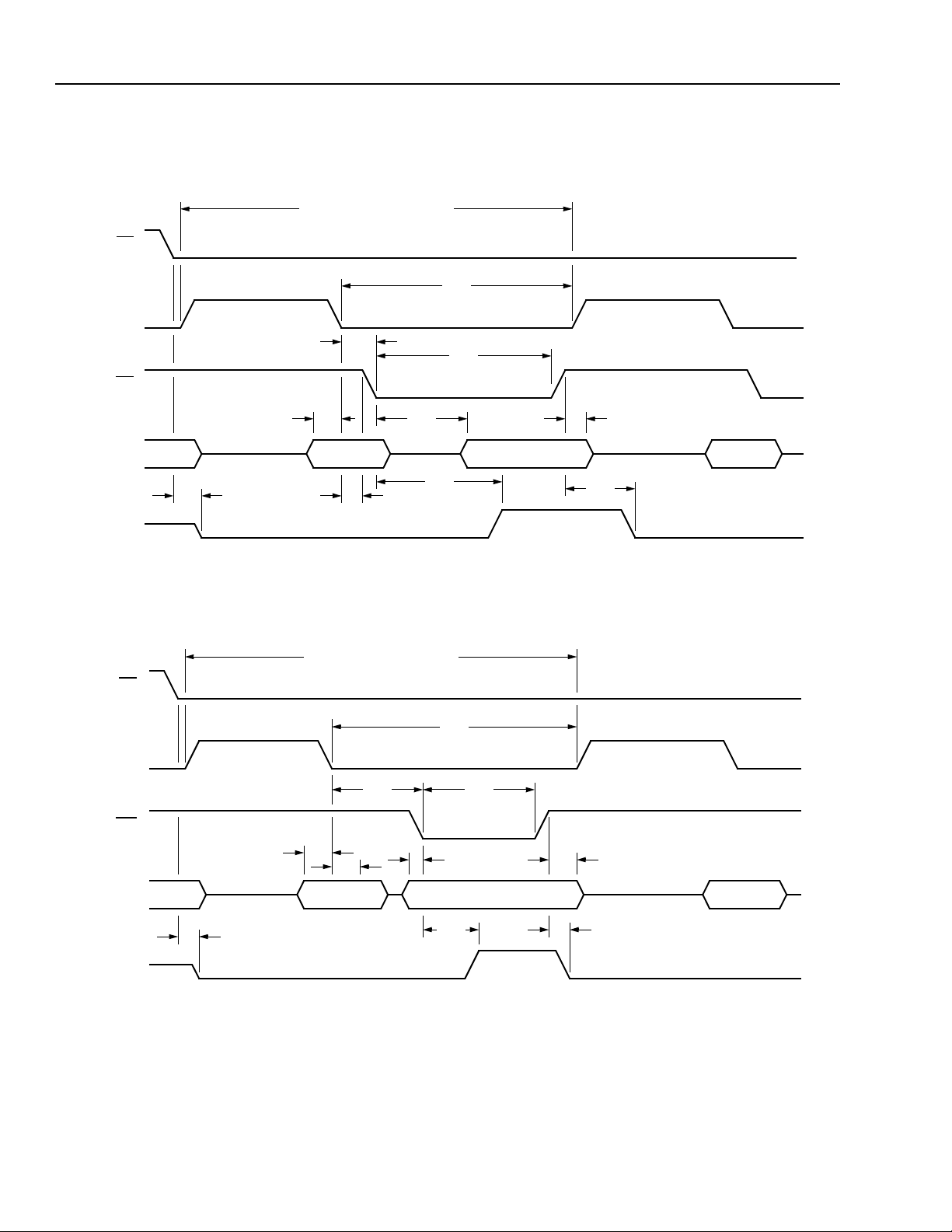
Data Sheet
(
)
(
)
)
)
TMPR28051 STS-1/AU-3 (STM-0) Mapper August 1999
Microprocessor Interface Description
CS
ALE
RD
RDY
continued
VALID
DATA
MINIMUM READ CYCLE
t21
t19
VALID
ADDRESS
t20t27
I/O Timing
AD[7:0]
continued
t32
t33
t22
t23
VALID DATA
t24
VALID
ADDRESS
t25
5-3691(F)r.12
Figure 9. Mode 4—Read Cycle Timing (MPMODE = 1, MPMUX = 1
MINIMUM WRITE CYCLE
CS
t32
ALE
t26 t34
WR
AD[7:0]
RDY
VALID
DATA
t27
t19
t20
VALID
ADDRESS
VALID DATA
t29
t31t28
t30
VALID
ADDRESS
5-3692(F)r.13
Figure 10. Mode 4—Write Cycle Timing (MPMODE = 1, MPMUX = 1
64 Lucent Technologies Inc.

Data Sheet
g
g
g
g
ge (
g
y
(
y
g
y
y (
)
g
g
g
g
g
g
g
)
(
)
(
)
August 1999 TMPR28051 STS-1/A U-3 (STM-0) Mapper
Absolute Maximum Ratings
Stresses in excess of the absolute maximum ratings can cause permanent or latent damage to the device. These
are absolute stress ratin
excess of those
in
s for extended periods can adversely affect device reliability.
iven in the operational sections of this device specification. Exposure to absolute maximum rat-
s only. Functional operation of the device is not implied at these or any other conditions in
Table 34. Absolute Maximum Ratin
Parameter S
Power Suppl
Input Volta
Output Volta
e Temperature T
Stora
Ambient Operatin
dc Voltage
eV
eV
Temperature RangeT
s
mbol Min Max Unit
DD
V
I
O
st
A
–0.5 4.6 V
–0.3 5.5 V
—3.63V
–65 125 °C
–40 85 °C
Handling Precautions
Although protection circuitry has been designed into this device, proper precautions should be taken to avoid exposure to electrostatic dischar
and char
ed-device model (CDM) for ESD-susceptibility testing and protection design evaluation. ESD voltage
thresholds are dependent on the circuit parameters used in the defined model. No industr
been adopted for the CDM. However, a standard HBM
and, therefore, can be used for comparison purposes. The HBM ESD threshold presented here was obtained b
usin
these circuit parameters.
Table 35. ESD Threshold Volta
Model Volta
HBM 2000
CDM
all pins except corner pins
all corner pins
CDM
ESD) during handling and mounting. Lucent employs a human-body model (HBM)
-wide standard has
resistance = 1500 Ω, capacitance = 100 pF) is widely used
e
e (volts
500
1000
65Lucent Technologies Inc.

Data Sheet
y
yp
y (
)
g
g
(
y
(
y
[
µ
y
g
g
g
µ
g
g
TMPR28051 STS-1/AU-3 (STM-0) Mapper August 1999
Operating Conditions
Table 36. Recommended Operating Conditions
Parameter S
Power Suppl
dc Voltage
Ground V
Input Volta
Input Volta
e, HighV
e, Low V
Ambient Temperature T
Power Dissipation, DS1
TA = 23 °C, VDD = 3.3 V):
Full Loopback
Broadcast
Standb
Power Dissipation, E1
TA = 23 °C, VDD = 3.3 V):
Full Loopback
Broadcast
Standb
Electrical Characteristics
Table 37. Logic Interface Characteristics
An internal 100 kΩ pull-up is provided on the ICT
RSTS1PAR, E1BLUECLK, RCLK
20
A. All buffers use CMOS levels.
28:1], and RDAT A[28:1] pins. This requires these input pins to sink no more than
mbol Min T
DD
V
SS
IH
IL
A
D
P
3.14 3.3 3.46 V
—0.0—V
—V
—VSS1.0 V
–40 — 85 °C
—
—
—
—
—
—
DD
– 1.0 5.25 V
380
380
360
450
450
430
Max Unit
—
—
—
—
—
—
, RESET, CS, TCK, TDI, TMS, TRST, RSTS1DATA[7:0],
mW
mW
mW
mW
mW
mW
Parameter S
Input Volta
e:
Low
Hi
h
Input Leaka
Output Volta
eIL——1.0
e:
Low
Hi
h
Input Capacitance C
Load Capacitance* C
* 100 pF allowed for AD[7:0] (pins 48 to 50 and 55 to 59).
mbol Test Conditions Min Max Unit
IL
V
IH
V
OL
V
OH
V
I
L
—
V
GND
DD
– 1.0
1.0
V
DD
V
V
A
–5.0 mA
5.0 mA
V
GND
DD
– 1.0
0.5
V
DD
V
V
— —3.0pF
— — 25 pF
66 Lucent Technologies Inc.

Data Sheet
g
(
g
)
August 1999 TMPR28051 STS-1/A U-3 (STM-0) Mapper
Timing Characteristics
Operational Timin
The operational timing parameters can be grouped separately for clocks, inputs, and outputs.
transmit and receive input clock specifications for this device.
descriptions in Table 1, pa
Table 38. Input Clock Specifications
Signal Name Parameter Min Max Unit
TSTS1CLKIN Frequency 51.839 51.841 MHz
Clock Pulse High Time 40 60 %
Peak-to-Peak Jitt er — 1 %
Frequency 19 .439 19.441 MHz
Clock Pulse High Time 40 60 %
Peak-to-Peak Jitt er — 1 %
Frequency 6 .479 6.481 MHz
Clock Pulse High Time 40 60 %
Peak-to-Peak Jitt er — 1 %
RCLK[1:28]
(DS1 Mode)
RCLK[1:21]
(E1 Mode)
RSTS1CLK Frequency 51.839 51.841 MHz
TCK
Frequency 1.5437 1.5443 MHz
Clock Pulse High Time 40 60 %
Peak-to-Peak Jitt er — 1 %
Frequency 2. 0484 2.0476 MHz
Clock Pulse High Time 40 60 %
Peak-to-Peak Jitt er — 1 %
Clock Pulse High Time 40 60 %
Peak-to-Peak Jitt er — 1 %
Frequency 0.5 12 MHz
Clock Pulse High Time 40 60 %
Peak-to-Peak Jitt er — 1 %
Rise/Fall Time — 15 ns
es 7—9.
Input Clock Signals
JTAG Signal
For definitions of the signal names, see the pin
Table 38 lists the
67Lucent Technologies Inc.

Data Sheet
(
)
(
)
g
g
g
TMPR28051 STS-1/AU-3 (STM-0) Mapper August 1999
Timing Characteristics
Operational Timing
continued
continued
Table 39 lists the setup time (tSU) and hold time (tH) specifications for the receive input and JTAG signals. The digital system interface timing is shown in Figure 11.
Table 39. Input Timing Specifications
Input Name Reference CLK
Setup Time
(t
)
*
SU
Hold Time
(tH)
Unit
Min Max Min Max
Receive Signals
TSTS1SYNC TSTS1CLKIN 5 — 2 — ns
RDATA[1:28] RCLK[1:28]
RSTS1DATA[7:0] RSTS1CLK
RSTS1PAR RSTS1CLK
RSTS1SERIAL RSTS1CLK
↑↓
↑↓
↑↓
↑↓
50 — 40 — ns
15 — 2 — ns
15 — 2 — ns
5—2—ns
JTAG Signal
TDI
*
These clock edges are programmable through the microprocessor interface.
Notes:
↑
represents a low-to-hi
↓
represents a hi
h transition.
h-to-low transition.
TCK
↑
50 — 50 — ns
CLOCK IN
DATA IN
CLOCK OUT
DATA OUT
SU
t
H
t
PD
t
Figure 11. Interface Data Timin
5-5342(F)r.5
68 Lucent Technologies Inc.

Data Sheet
g
)
g
August 1999 TMPR28051 STS-1/A U-3 (STM-0) Mapper
Timing Characteristics
(continued)
Operational Timin
The output clock specifications are shown in Table 40.
Table 40. Output Clock Specifications
Signal Name Frequency
TCLK[1:28]
(DS1 Mode)
TCLK[1:28]
(E1 Mode)
TSTS1CLKOUT
*
The duty-cycle distortion added to the TSTS1CLKOUT signal is ≤2% worst case when measured from 1.5 V in to 1.5 V out with a 2 ns rise
time input.
1.544 MHz ± 5% CL = 50 pF — 30 — 30 ns
2.048 MHz ± 5% CL = 50 pF — 30 — 30 ns
*
51.84 MHz ± 5% CL = 15 pF — 3 — 3 ns
19.44 MHz ± 5% C
6.48 MHz ± 5% CL = 15 pF — 3 — 3 ns
(continued)
Rise Time Fall Time
Test
Conditions
R
t
F
Min Max Min Max
= 15 pF — 3 — 3 ns
L
Unitt
Table 41 lists the propagation delay (t
shown in Fi
ure 11, page 68.
PD
Table 41. Output Timing Specifications
Output Name Reference CLK
TDATA[28:1]
TSTS1DATA[7:0] TSTS1CLKIN
TSTS1PAR TSTS1CLKIN
TSTS1DATA7
TDO
* Propagation delay skew, t
Notes:
↑
represents a low-to-high transition.
↓
represents a high-to-low transition.
TCLK[1:28]
TSTS1CLKIN
↓
TCK
PLH—tPHL,
is ±200 ps.
↑↓
↑
↑
↑
specifications for the output signals. The digital system interface timing is
T est
Conditions
Propagation Delay
PD
*
Unitt
Min Max
Transmit Signals
CL = 25 pF 40 190 ns
C
= 15 pF 2 12 ns
L
C
= 15 pF 2 12 ns
L
CL = 15 pF 0 3.5 ns
JTAG Signal
= 50 pF 1.5 17 ns
C
L
69Lucent Technologies Inc.

Data Sheet
g
g
y
g
g
TMPR28051 STS-1/AU-3 (STM-0) Mapper August 1999
Timing Characteristics
(continued)
Tr ansmit Sync Timin
In all transmit modes, the first bit/byte of the J0, J1, and V1 bytes are coincident with the sync pulse. The second
and third pulses in this composite si
pulses as shown below, then V1
TSTS1CLK
TSTS1SYNC
nal are only needed to force V1 superframe alignment. If there are three sync
will
be forced. The serial mode transmit s
nc timing is shown below in Figure 12.
TSTS1DATA
Note: The - symbol followed by a number represents the bit number in the byte.
J0-7 J0-6 J0-5 J0-4 J0-3 J0-2 J0-1 J0-0 J1-7 J1-6 J1-5 J1-4 J1-3 J1-2 J1-1 J1-0 V1-7 V1-6 V 1-5 V1-4 V1-3 V1-2 V1-1 V1-0
Figure 12. Serial Mode Transmit Sync Timin
The bus mode transmit sync timing is shown below in Figure 13.
TSTS1CLK
TSTS1SYNC
TSTS1DATA
Note: The # symbol followed by a number represents the active device on the bus.
J0#1 J 0#2 J0#3 J1#1 J1#2 J1#3 V1#1 V1#2 V1#3
Figure 13. Bus Mode Transmit Sync Timin
5-6347(F)r.1
5-6347(F).a
70 Lucent Technologies Inc.

Data Sheet
(
)
g
y
g
August 1999 TMPR28051 STS-1/A U-3 (STM-0) Mapper
Timing Characteristics
(continued)
Tr ansmit Sync Timing
continued
The nonbus parallel mode transmit sync timing is shown below in Figure 14.
TSTS1CLK
TSTS1SYNC
TSTS1DATA
J0 J1 V1
5-6347(F).b
Figure 14. Nonbus Parallel Mode Transmit Sync Timin
Receive Sync Timing
The only receive mode that requires a sync pulse is the bus mode. The sync pulse is required to align the device to
time slot #1. The bus parallel mode receive s
RSTS1CLK
nc timing is shown below in Figure 15.
RSTS1SERIAL
RSTS1DATA
Note: The # symbol followed by a number represents the active device on the bus.
J0#1 J0 #2 J0#3 J1#1 J1#2 J1#3 V1#1 V1#2 V1#3
Figure 15. Bus Parallel Mode Receive Sync Timin
5-6347(F).cr.1
71Lucent Technologies Inc.

Data Sheet
g
TMPR28051 STS-1/AU-3 (STM-0) Mapper August 1999
Typical Uses
Path Termination Multiplex
Using the device without internal loopbacks results in an SDH/SONET path terminating multiplex, as shown in
Fi
ure 16.
TMPR28051
VT
GENERATE
SPE
GENERATE
SPE
INSERTION
LOGIC
STS-1 OUT
TMUX03155
STS/STM
MUX
LOGIC
DS1/E1 #1 IN
DS1/E1 #1 OUT
T7693
QUAD LIU
LIU
ELASTIC
STORE
DS1/E1 #n IN
LIU
DS1/E1 #n OUT
Note: n represents 28 or 21 for DS1 or E1, respectively.
ELASTIC
STORE
JITTER
ATTENUATE
JITTER
ATTENUATE
VT
GENERATE
VT
TERMINATE
VT
TERMINATE
SPE
DROP
LOGIC
SPE
LOCATE
SPE
TERMINATE
STS-1 IN
Figure 16. SDH/SONET Path Termination Multiplex Application
Digital Cross Connect
Using the device with STS-1 internal loopbacks results in a digital cross connect, as shown in Figure 17.
TMPR28051
SPE
T7693
QUAD LIU
GENERATE
T7693
QUAD LIU
STS/STM
DEMUX
LOGIC
5-4876(F)r.9
DS1/E1
#1 IN
DS1/E1
#n IN
Note: n represents 28 or 21 for DS1 or E1, respectively.
LIU
LIU
ELASTIC
STORE
ELASTIC
STORE
VT
GENERATE
VT
GENERATE
SPE
INSERTION
LOGIC
SPE
LOCATE
SPE
TERMINATE
SPE
DROP
LOGIC
VT
TERMINATE
VT
TERMINATE
LIU
LIU
DS1/E1
#1 OUT
DS1/E1
#n OUT
5-4878(F)r.8
Figure 17. Digital Cross Connect Application
72 Lucent Technologies Inc.

Data Sheet
(
)
(
g
August 1999 TMPR28051 STS-1/A U-3 (STM-0) Mapper
Typical Uses
continued
Test Pattern Use—Complete System
The internal test pattern generator can be used in conjunction with DS1 or E1 LIU devices that have built-in loopbacks
such as the Lucent T7698FL3/T7693) to do a complete system test, as shown in Figure 18.
TMPR28051
MAPPER
TEST
PATTERN
DROP
LOOPBACK
DS1/E1 IN
DS1/E1 AIS
LIU
LOOPBACK
MODE
TMPR28051
MAPPER
TEST
PATTERN
DROP
TEST PATTERN SOURCE
TEST
PATTERN
INSERT
OPTIONAL TEST PA TT ERN DROP
LIU
DS1/E1 AIS
DS1/E1 IN
MODE
5-4879(F)r.7
Figure 18. Test Pattern Usage for Complete System
Test Pattern Use—End to End
The internal test pattern generator can be used to test connectivity within a link by setting up a test pattern insertion at one end and a drop at the other, as shown in Fi
ure 19.
TMPR28051
MAPPER MAPPER
TEST
PATTERN
INSERT
TEST PATTERN SOURCE
TMPR28051
TEST
PATTERN
DROP
TEST PATTERN DROP
Figure 19. Test Pattern Usage for End-to-End Operation
5-4880(F)r.7
73Lucent Technologies Inc.

Data Sheet
TMPR28051 STS-1/AU-3 (STM-0) Mapper August 1999
Outline Diagram
208-Pin SQFP
Dimensions are in millimeters.
30.60 ± 0.20
28.00 ± 0.20
PIN #1 IDENTIFIER ZONE
1
52
53 104
157208
156
28.00
± 0.20
30.60
± 0.20
105
0.50 TYP
GAGE PLANE
SEATING PLANE
DETAIL BDETAIL A
0.25 MIN
1.30 REF
0.25
0.50/0.75
DETAIL A
3.40 ± 0.20
0.17/0.27
4.10 MAX
DETAIL B
SEATING PLANE
0.08
0.090/0.200
M
0.10
5-2196(F)r.14
74 Lucent Technologies Inc.

Data Sheet
p
g
g
g
g
g
g
g
g
g
g
g
q
g
[
g
g
g
g
g
g
g
g
g
(
)
g
p
(
)
August 1999 TMPR28051 STS-1/A U-3 (STM-0) Mapper
Ordering Information
Device Code Packa
TMPR28051-3-SL5 208-Pin SQFP –40 °C to +85 °C 108421678
DS99-068SONT Re
1. Page 1, added bulleted items concerning 3.3 V operation, and alarm and control standards.
2. Pa
3. Pa
4. Pa
5. Pa
6. Pa
7. Pa
8. Pa
9. Pa
10. Pa
e5, Description (continued) section, replaced the Lucent T7690/T7693 Quad Line Transceiver interfacing
device with the Lucent T7698FL3/T7693 Quad Line Transceiver.
e5, Figure 1, Block Diagram, clarified block flow.
e 6, changed pin 184 and all corresponding references to TCK.
e 7, clarified Pin 102.
e10, organized Nomenclature Assumptions section from the text at the beginning of the Description sec-
tion.
e 10—page 19, clarified block descriptions.
e 14, 2nd paragraph, corrected the explanation of the reduced H4 coding sequence format from “alternate
between” to “take on the followin
e 23—page 36, updated register map.
e37—page 59, updated register description text and placed text in tables.
laces DS98-100TIC to Incorporate the Following Updates
eTem
values.”
erature Comcode
Ordering Number
11. Pa
12. Pa
13. Pa
14. Pa
15. Pa
16. Pa
17. Pa
18. Pa
19. Pa
20. Pa
21. Pa
22.
e42, Table, Registers 0x00—0x16: Device-Level Control, Alarm, and Mask Bits, corrected the test pat-
tern se
VT_DROP
ues.
and E1.
uence for register XMT_PAT-0, bits 01 and 11 combinations.
e 49, Table 18, Registers 0x33—0x4E: VT Drop Selection, corrected VTxDROP, bits 4 through 0, to
4:0]_[1:28].
e 54, Table 24, Registers 0x8A—0x8F: Digital Jitter Attenuator Controls, added the register default val-
e 65, Table 34, Absolute Maximum Ratings, updated table, including input and output voltages.
e 65, Table 35, ESD Threshold Voltage, added parameters and values.
e 66, Table 36, Recommended Operating Conditions, updated to list 3.3 V power dissipation for DS1
e 67, Table 38, Input Clock Specifications, added to the document.
e 69, Table 40, Output Clock Specifications, added to the document.
e 70, Transmit Sync Timing section, expanded and corrected.
e71, Figure 15, Bus Parallel Mode Receive Sync Timing, corrected pin name.
e 75, updated device code.
TMPR28051 STS-1/AU-3 (STM-0) Mapper Device Advisory for Version 2 of the Device
TMPR28051 STS-1/AU-3 (STM-0) Mapper Device Advisory for Version 3 of the Device
TMPR28051 STS-1/AU-3 (STM-0) Mapper Device Advisory for Version 4 of the Device
TMPR28051 STS-1/AU-3 (STM-0)
version 4, each published in April 1999,
DA99-009SONT
. An advisory was not issued for version 1 of the device.
Data Addendum, included all printed advisories and an addendum through
AY99-026SONT, AY99-027SONT, AY99-028SONT,
,
,
,
75Lucent Technologies Inc.

Data Sheet
TMPR28051 STS-1/AU-3 (STM-0) Mapper August 1999
For additional information, contact your Microelectronics Group Account Manager or the following:
INTERNET: http://www.lucent.com/micro
E-MAIL: docmaster@micro.lucent.com
N. AMERICA: Microelectronics Group, Lucent Technologies Inc., 555 Union Boulevard, Room 30L-15P-BA, Allentown, PA 18103
ASIA PACIFIC: Microelectronics Group, Lucent Technologies Singapore Pte. Ltd., 77 Science Park Drive, #03-18 Cintech III, Singapore 118256
CHINA: Microelectronics Group, Lucent Technologies (China) Co., Ltd., A-F2, 23/F, Zao Fong Universe Building, 1800 Zhong Shan Xi Road,
JAPAN: Microelectronics Group, Lucent Technologies Japan Ltd., 7-18, Higashi-Gotanda 2-chome, Shinagawa-ku, Tokyo 141, Japan
EUROPE: Data Requests: MICROELECTRONICS GROUP DATALINE: Tel. (44) 7000 582 368, FAX (44) 1189 328 148
Lucent Technologies Inc. reserves the right to make changes to the product(s) or information contained herein without notice. No liability is assumed as a result of their use or application. No
rights under any patent accompany the sale of any such product(s) or information.
Copyright © 1999 Lucent Technologies Inc.
All Rights Reserved
1-800-372-2447, FAX 610-712-4106 (In CANADA: 1-800-553-2448, FAX 610-712-4106)
Tel. (65) 778 8833, FAX (65) 777 7495
Shanghai 200233 P. R. China Tel. (86) 21 6440 0468, ext. 316, F A X ( 86) 21 6440 0652
Tel. (81) 3 5421 1600, FAX (81) 3 5421 1700
Technical Inquiries: GERMANY: (49) 89 95086 0 (Munich), UNITED KINGDOM: (44) 1344 865 900 (Ascot),
FRANCE: (33) 1 40 83 68 00 (Paris), SWEDEN: (46) 8 600 7070 (St oc kh olm), FI NLAN D: (358) 9 43 54 28 00 (Helsinki),
ITALY: (39) 02 6608131 (Milan), SPAIN: (34) 1 807 1441 (Madrid)
August 1999
DS99-068SONT (Replaces DS98-100TIC)
 Loading...