


Advisory
September 2001
Ambassador
®
T8110
Version History
Introduction
The purpose of this advisory is to provide information on the different versions of the
Ambassador
T8110.
T8110 Version 1
Models of the T8110 V1 had two device issues. The two device issues only affect the microprocessor interface
and packet switching capabilities. The T8110 V1 can function as a 4096 connection standard telephony switch
when using the PCI interface.
Issue 1: Microprocessor interface: The RDY(DTACKn) signal can oscillate if the microprocessor device
driving the microprocessor interface does not relinquish its RDn (or WRn) signal within one
65 MHz clock cycle after the reassertion of RDY (
Intel
®
mode) or deassertion of DTACKn
(
Motorola
®
mode).
Workaround: The processor or board-level component driving the microprocessor port must deassert RDn
or WRn immediately (within 15 ns) upon reassertion of RDY.
Issue 2: Packet switch malfunction: The T8110 does not disable its upper byte lanes on the descriptor
table update, resulting in an over-write of descriptor table data. The descriptor table update
occurs as the last phase of a PCI Master PUSH & PULL cycle. This results in virtual channel
connection malfunctions. TDM switching is unaffected.
Workaround: A systemic workaround for the user is to keep a shadow table for the UOR portion of the
descriptor table.
T81 10 version 1 models can be identified by the markings on the device or by reading the version ID register. If
the last line of the device markings is a 7 digit number followed by no version number, then the device is a version 1. Reading the version ID register 0x00128 will read back a value of 01h, indicating the device is version
1.
Samples of version 1 are no longer available (version 2 samples are now available).
T8110 Version 2
Models of the T8110 V2 have one device issue. The device issue only affects the packet switching capabilities.
The T8110 V2 can function as a 4096 connection standard telephony switch when using either PCI or microprocessor interface.
Issue 1 (from version 1): Fixed. The microprocessor interface issue has been resolved.
Issue 2 (from version 1): Will be fixed in version 3.
T81 10 version 2 models can be identified by the markings on the device or by reading the version ID register. If
the last line of the device markings is a 7 digit number followed by V2, then the device is a version 2. Reading
the version ID register 0x00128 will read back a value of 02h, indicating the device is a version 2.
Samples of version 2 are currently available.
For additional information, contact your local FAE (field application engineer), or call 1-800-372-2447.

Agere Systems Inc. reserves the right to make changes to the product(s) or information contained herein without notice. No liability is assumed as a result of their use or application.
Copyright © 2001 Agere Systems Inc.
All Rights Reserved
September 2001
AY01-038CTI (Replaces AY01-021CTI and must accompany DS00-434CTI)
For additional information, contact your Agere Systems Account Ma nager or the following:
INTERNET: http://www.agere.com
E-MAIL: docmaster@agere.com
N. AMERICA: Agere Systems Inc., 555 Union Boulevard, Room 30L-15P-BA, Allentown, PA 18109-3286
1-800-372-2447, FAX 610-712-4106 (In CANADA: 1-800-553-2448, FAX 610-712-4106)
ASIA: Agere Systems Hong Kong Ltd., Suites 3201 & 3210-12, 32/F, Tower 2, The Gateway, Harbour City, Kowloon
Tel. (852) 3129-2000, FAX (852) 3129-2020
CHINA: (86) 21-5047-1212 (Shangha i) , (86) 10-6522-5566 (Beijing), (86) 755-695-7224 (Shenzhen)
JAPAN: (81) 3-5421-1600 (Tokyo), KOREA: (82) 2-767-1850 (Seoul), SINGAPORE: (65) 778-8833, TAIWAN: (886) 2-2725-585 8 (Taipei)
EUROPE: Tel. (44) 7000 624624, FAX (44) 1344 488 045
Intel
is a registered trademark of Intel Corporation.
Motorola
is a registered trademark of Motorola, Inc.

Data Sheet
May 2001
Ambassador
®
T8110 PCI-Based H.100/H.110 Switch
and Packet Payload Engine
1 Introduction
The T8110 is Agere Systems Inc.’s newest addition
to the
Ambassador
series of computer telephony
integrated circuits. This device not only has the capabilities of previous members of the
Ambassador
series but al so extends them by providing a flexible
interface for switching packet payloads between a
local PCI bus and the H.100/H.110 buses. Packets
may also be switched between the local PCI bus and
local TDM streams. This part is intended to work with
a coprocessor for providing header, framing, and
checksum generation. Since the T8110 operates
purely on payloads, multiple protocols such as IP,
ATM, and A-Bis can therefore be supported simultaneously. To re duce sy st em in t egration costs, sup port
for non-PCI devices is provided through a minibridge.
1.1 Features
n
4,096-connection unified switch
n
Packet payload engine suppor ts up to 512 virt ual
channels
n
Full H.100/H.110 support (32 data lines, all clock
modes)
n
32 local I/O lines (2, 4, 8, or 16 Mbits/s)
n
PCI interface: combined master/slave with burst
n
Microprocessor interface:
Motorola*/Intel
†
modes
n
Minibridge with programmable chip selects
n
Interrupt controller with external inputs
n
Eight independent general-purpose I/O lines
n
Eight independently programmed framing signals
n
Four local clocks
n
T1/E1 rate adaptation
n
Two clock-fallback modes
n
Stratum 4/4E and AT&T 62411 MTIE compliant
n
Incorporates 38 H.100 and 34 H.110 termination
resistors
n
Subrate switching of 4 bits, 2 bits, or 1 bit
n
Backward compatible to all T810x devices
n
JTAG/boundary-scan testing support
n
BSDL files available
n
Assists H.110 hot swap
n
Single 3.3 V supply with 5 V tolerant inputs and
TTL compatible outputs
n
272 PBGA package
n
Evaluation boards available, PCI and
CompactPCI
‡
Hot Swap
5-8921F
Figure 1. Basic Application of the T8110 as a CT
Switch and CT-IP Payload Processor
FRAMERS
AGERE
T8110
COPROCESSOR
ETHERNET
MAC/PHY
MEMORY
PCI-PCI
BRIDGE
TRUNKS
STREAMS
BRIDGE
I/F
STREAMS
& CLOCKS
PCI
10/100
H.100 BUS
LOCAL PCI BUS
HOST PCI BUS
PCI
PCI
PCI
* Motorola
is a registered trademark of Motorola, Inc.
†
Intel
is a registered trademark of Intel Corporation.
‡
CompactPCI
is a registered trademark of the PCI Industrial Computer Manufacturers Group.

Table of Contents
Contents Page
2 Agere Systems Inc.
Data Sheet
May 2001
and Packet Payload Engine
Ambassador
T8110 PCI-Based H.100/H.110 Switch
1 Introduction ............................................................................................................................................................1
1.1 Features .......................................................................................................................................................... 1
2 Pin Description ...................................................................................................................................................... 8
2.1 Interface Signal s .............................................................................................................................................8
2.2 T8110 P inout Inform ation ............................................................................................................................. 11
2.3 Special Buffer Req uir e me n ts ......... ................. ................ ................. ................ ................. ........................ ....18
2.3.1 H1x0 Bus Signal Internal Pull-Up/Pull-Down ................................................................................... 18
2.3.2 Lo cal Bus Signal Internal Pull-Up .................................................................................................... 18
3 Main Architect u r a l Fea tures .................... ................ ................. ................ ................. ................ ................. .........19
3.1 T8110 A rchite cture .......................................................................................................................................19
4 PCI Interface .......................... ................. ................ ................. ................ ................. ....................... ................. ..22
4.1 Target ...........................................................................................................................................................22
4.1.1 PCI Interface Registers .................................................................................................................... 23
4.1.2 Register Space Target Access ........................................................................................................29
4.1.3 Connection Memory Space Target Access .....................................................................................29
4.1.4 Data Memory Space Target Access ................................................................................................29
4.1.4.1 Posted Write Transaction ....................................................................................................29
4.1.4.2 Delayed Read Transact ion ....................... ................ ................. ................ ................. ....... ..30
4.1.5 Virtual Chann el Memory Space Target Access ...............................................................................30
4.1.5.1 Posted Write Transaction ....................................................................................................30
4.1.5.2 Delayed Read Transact ion ....................... ................ ................. ................ ................. ....... ..30
4.1.6 Mini bridge Spac e Target Access . .................................................................................................... 30
4.1.6.1 Posted Write Transaction ....................................................................................................31
4.1.6.2 Delayed Read Transact ion ....................... ................ ................. ................ ................. ....... ..31
4.2 Initiator ..........................................................................................................................................................31
4.2.1 PUSH Operation (Upstream Transaction) .......................................................................................31
4.2.2 PULL Operation (Downstream Transaction) ....................................................................................32
4.3 Configuration Space/EEPROM Interface ......................................................................................................34
4.3.1 Loadable PCI Configuration Space Via EEPROM ...........................................................................36
5 Microproce sso r In te r face .................... ................ ................. ................. ......... ................. ....... ......... ................. ....38
5.1
Intel/Motorola
Protocol Sele ctor ............ .......... ................ ................. ................ ................. ................. ...........38
5.2 Word/Byte Addressing Selector ............... ......... ................. ................ ................. ................ ....... .......... .........38
5.3 Access Via the Microprocessor Bus .............................................................................................................39
5.3.1 Microprocessor Interface Register Map ...........................................................................................40
5.3.2 Register Space Access ....................................................................................................................44
5.3.3 Connection Memor y Sp ace Access ............ ................. ................ ................. ................ ...................44
5.3.4 Data Memory Space Access ...........................................................................................................45
5.3.5 Virtual Chann el Memory Space Access .......................................................................................... 45
6 Operating Control and Status ..............................................................................................................................46
6.1 Control Registers ..........................................................................................................................................46
6.1.1 Reset Registers ...............................................................................................................................46
6.1.2 Master Output Enable Register .......................................................................................................47
6.1.3 Con nection Control—V irtual Chann el Enable and Data Memory Selector Register ........................48
6.1.4 General Clock Control (Phase Alignment, Fallback, Watchdogs) Register .................. .......... ....... ..49
6.1.5 Phase Alignment Select Register ....................................................................................................50
6.1.6 Fallback Control Register ................................................................................................................ 50
6.1.7 Fallback Type Select Register .........................................................................................................51
6.1.8 Fallback Trigger Registers ............................................................................................................... 51
6.1.9 W atchdo g Select, C8, and NETREF Registers ................................................................................52

Table of Contents (continued)
Contents Page
Agere Systems Inc. 3
May 2001 and Packet Payload Engine
Data Sheet
Ambassador
T8110 PCI-Based H.100/H.110 Switch
6.1.10 Watchdog EN Register ....................................................................................................................53
6.1.11 F ailsafe Control Registers ................................................................................................................ 54
6.1.12 External Buffers—Descriptor Table Base Address ..........................................................................55
6.2 Error and Status Registers ...........................................................................................................................55
6.2.1 Clock Errors .....................................................................................................................................56
6.2.1.1 Transient Clock Errors Registers ......................................................................................... 56
6.2.1.2 Latched Clock Error Register ..............................................................................................57
6.2.2 System Status ..................................................................................................................................58
6.2.3 Clock Fallback Status Register ........................................................................................................58
6.2.4 PLL and S witch ing Status Registe r . .................................................................................................58
6.2.5 System Errors Register ....................................................................................................................59
6.2.6 Device Identification Registers .........................................................................................................60
6.2.7 Misc ellaneous Status .......................................................................................................................61
7 Clock Architecture ...............................................................................................................................................62
7.1 Clock Input Control Registers ....................................................................................................................... 63
7.1.1 Main Input Selector Register ........................................... ....... .......... ....... .. ....... .......... .. ..... ...............63
7.1.2 Main Divider Register .......................................................................................................................64
7.1.3 Analog PLL1 (APLL1) Input Selector Register ................................... ..... ....... ....... ....... ..... ....... ..... ...64
7.1.4 APLL1 Rat e Register . ......................................................................................................................65
7.1.5 Main Inversion Select Register ........................................................................................................65
7.1.6 Resource Divider Register ...............................................................................................................66
7.1.7 Analog PLL2 (APLL2) Rate Register ................................... .. .......... ....... ....... .. .......... ....... .. .............66
7.1.8 LREF Input Select Registers ................................................ .. .......... ....... .. ....... .......... ....... ...............67
7.1.9 DPLL1 Input Selector .......................................................................................................................68
7.1.9.1 DPLL1 Rate Register ...........................................................................................................68
7.1.10 DPLL2 Input Selector ................................... .......... .. ....... ....... ..... ....... ....... ....... ..... ....... ....................69
7.1.10.1 DPLL2 Rate Register ...........................................................................................................69
7.1.11 NET REF1 Registers ........................................................................................................................70
7.1.12 NET REF2 Registers ........................................................................................................................71
7.2 Clock Output Control Registers ....................................................................................................................72
7.2.1 Master Output Enables Register ......................................................................................................72
7.2.2 Clock Output Format Registers ........................................................................................................74
7.2.3 TCLK and L_SCx Select Registers ..................................................................................................74
7.3 Clock Register Access ..................................................................................................................................76
7.4 Clock Circuit Operation—A P LL1 ..................................................................................................................76
7.4.1 Main Clock Selection, Bit Clock, and Frame .................................................... .......... .. ....... ........ .....76
7.4.1.1 Watchdog Timers ................................................................................................................77
7.4.1.2 Frame Center Sampling ......................................................................................................78
7.4.2 Main and Resource Dividers ............................................................................................................78
7.4.3 DPLL1 .............................................................................................................................................. 79
7.4.4 Reference Selector ..........................................................................................................................79
7.4.5 Internal Clock Generation ................................................................................................................ 79
7.4.5.1 Phase Alignment .......... ................. ................. ................ ................. ................ ................. ...80
7.5 Clock Circuit Operation, APLL2 ....................................................................................................................81
7.5.1 DPLL2 .............................................................................................................................................. 81
7.6 Clock Circuit Operation, CT_NETR EF Generation .......................................................................................81
7.6.1 NETREF Source Select ...................................................................................................................81
7.6.2 NETREF Divider ..............................................................................................................................81
7.7 Clock Circuit Operation—Fa llback and Fai lsafe ........................................................................................... 82

Table of Contents (continued)
Contents Page
4 Agere Systems Inc.
Data Sheet
May 2001
and Packet Payload Engine
Ambassador
T8110 PCI-Based H.100/H.110 Switch
7.7.1 Clock Fallback .................................................................................................................................82
7.7.1.1 Fallback Events ...................................................................................................................82
7.7.1.2 Fallback Scenarios—Fixed vs. Rotating Secondary ............................................................83
7.7.1.3 H-Bu s Clock Enable/Disabl e on Fallback ............................................................................86
7.7.2 Clock Failsafe ..................................................................................................................................88
7.7.2.1 Failsafe Events .......... ................ .......... ................. ................ ................. ................ . .............88
8 Frame Group and FG I/O .................................................................................................................................... 90
8.1 Frame Group Control Re gisters ............ ................. ................ ................. ................. ....................... ..............90
8.1.1 FGx Lower and Upper Start Registers ............................................................................................. 90
8.1.2 FGx Width Registers ........................................................................................................................ 91
8.1.3 FGx Rate Registers .........................................................................................................................91
8.2 FG7 Timer Option .........................................................................................................................................92
8.2.1 FG7 Count er (Low and High Byte) Registers ..................................................................................92
8.3 FGIO Control Registers ................................................................................................................................ 93
8.3.1 FGIO Data Register .........................................................................................................................93
8.3.2 FGI O Read Ma sk Register .............................................................................................................. 93
8.3.3 FGIO R/W Register .......................................................................................................................... 94
8.4 FG Circuit Operation .....................................................................................................................................95
8.4.1 Frame Group 8 kHz Reference Generation .....................................................................................96
8.4.2 FGIO General-Purpose Bits .............................................................................................................97
8.4.3 Programmable Timer (FG7 Only) .................................................................................................... 97
8.4.4 FG External Interrupts .....................................................................................................................97
8.4.5 FG Diagnostic Test Point Observation .... ........................................................................................97
9 General-Purpose I/O . .......................................................................................................................................... 98
9.1 GPIO Control Registers ................................................................................................................................ 98
9.1.1 GPIO Data Register .........................................................................................................................98
9.1.2 GPIO Read Mask Register ..............................................................................................................99
9.1.3 GPIO R/W Register .........................................................................................................................99
9.1.4 GPIO Override Register .................................................................................................................100
9.2 GP Circuit Operation ...................................................................................................................................100
9.2.1 GPIO General-Purpose Bits ..........................................................................................................101
9.2.2 GP Dual-Purpose Bits GPIO (Override) .........................................................................................1 01
9.2.2.1 GP H.110 Clock Master Indicators (GP0, GP1 Only) ........................................................101
9.2.2.2 PCI_RST# Indicator (GP2 Only) ........................................................................................101
9.2.3 GP External Interrupts ...................................................................................................................101
9.2.4 GP Diagnostic Test Point Observation ..........................................................................................101
10 Stream Rate Control .......................................................................................................................................1 02
10.1 H-Bus Stream Rate Control Registers ...................................................................................................103
10.1.1 H-Bus Rate Registers ....................................................................................................................103
10.2 L-Bus Stream Rate Control Registers ...................................................................................................103
10.2.1 L-Bus Rate Registers ..................................................................................................................... 1 03
10.2.2 L-Bus 16.384 Mbits/s Operation ....................................................................................................104
10.2.3 16 .384 Mbits/s Local I/O Superrate ...............................................................................................105
11 Minibridge ........................................................................................................................................................107
11.1 W ait-State Control Registers .................................................................................................................107
11.1.1 Minibridge Wait-State Control Registers .. ......................................................................................107
11.2 Strobe Control Registers .......................................................................................................................110
11.3 Minibridge Circuit Operation .................................................................................................................. 1 10
11.4 Minibridge Operational Addressing .......................................................................................................1 12

Table of Contents (continued)
Contents Page
Agere Systems Inc. 5
May 2001 and Packet Payload Engine
Data Sheet
Ambassador
T8110 PCI-Based H.100/H.110 Switch
12 Error Reporting and Interrupt Control ..............................................................................................................113
12.1 Interrupt Control Registers ....................................................................................................................113
12.1.1 Interrupts Via External FG[7:0] Registers ......................................................................................113
12.1.1.1 FGIO Interrupt Pending Register ........................................... ....... ..... ....... ....... ..... ....... ..... .113
12.1.2 Interrupts Via External GP[7:0] ......................................................................................................115
12.1.2.1 GPIO Interrupt Pending Register .......................................................................................115
12.1.2.2 GPIO Edge/Level and GPIO Polarity Registers ................................................................1 16
12.1.3 Interrupts Via Internal System Errors .............................................................................................116
12.1.4 System Interrupt Pending High/Low Registers ..............................................................................117
12.1.5 System Interrupt Enable High/Low Registers ................................................................................118
12.1.6 Interrupts Via Internal Clock Errors ................................................................................................ 1 19
12.1.7 Cl ock Interrupt Pending High/Low Registers ................................................................................. 1 20
12.1.8 Cl ock Interrupt Enable High/Low Registers ...................................................................................121
12.1.9 Interrupt Servicing Registers ..........................................................................................................1 22
12.1.9.1 Arbitration Control Register ...............................................................................................122
12.1.10 PCI_INTA Output Select Register ..................................................................................................122
12.1.10.1 SYSERR and CLKERR Output Select Register ................................................................122
12.1.10.2 Interrupt In-Service Registers ...........................................................................................123
12.2 Error Reporting and Interrupt Controller Circuit Operation ....................................................................125
12.2.1 Externally Sourced Interrupts Via FG[7:0], GP[7:0] .......................................................................126
12.2.2 Internally Sourced System Error Interrupts ....................................................................................126
12.2.3 Internally Sourced Clock Error Interrupts .......................................................................................126
12.2.4 Arbitration of Pending Interrupts ....................................................................................................126
12.2.4.1 Arbitration Off .................... ................. ................ ................. ................ ........................ ......126
12.2.4.2 Flat Arbitration ...................................................................................................................126
12.2.4.3 Tier Arbitration ...................................................................................................................1 26
12.2.4.3.1 Pre-Empting Disabled ..................................................................................127
12.2.4.3.2 Pre-Empting Enabled ..................................................................................127
12.2.5 CLKERR Output .............................................................................................................................127
12.2.6 SYSERR Output ....... ......... ................. ................. ................ ................. ................ ................. ........127
12.2.7 PCI_INTA# Output ............................ ................ ................. ................ ................. ........................ ...127
12.2.8 System Handling of Interrupts ........................................................................................................ 127
13 Test and Diagnostics ..................................................... ..... ....... ....... ..... ....... ....... ....... ..... ................. ...............128
13.1 Diagnostics Control Registers ...............................................................................................................128
13.1.1 F G Testpoint Enable Register ........................................................................................................128
13.1.2 GP Testpoint Enable Register .......................................................................................................129
13.1.3 State Counter Modes Registers .....................................................................................................132
13.1.4 Miscellaneous Diagnostics Low Register .................................... ..... .. ..... .. ..... .. ..... ..... .. ..... .. ..... . .....133
13.1.5 External Buffer Retry Timer Register ............................................................................................. 1 34
13.2 Diagnostic Circuit Operation .................................................................................... ..............................135
14 Connection C ontrol—St andard and Virtual Channel ......................................................................................136
14.1 Programming Interface .......................................................................................................................... 1 36
14.1.1 PCI Interface .................... ................. ................ ................. ................ ................. ........................ ...136
14.1.1.1 PCI Connection Memory Programming .............................................................................136
14.1.1.2 PCI Virtual Channel Memory Programming . .....................................................................138
14.1.2 Microproce sso r In te rface .................... ................. ................ ................. ................ ........................ .139
14.1.2.1 Microprocessor Connection Memory Programming .................................................... ......139
14.1.2.2 Microprocessor Virtual Channel Memory Programming ............................................... 144
14.2 Switching Operation ..............................................................................................................................1 46

Table of Contents (continued)
Contents Page
6 Agere Systems Inc.
Data Sheet
May 2001
and Packet Payload Engine
Ambassador
T8110 PCI-Based H.100/H.110 Switch
14.2.1 Memory Architecture and Configuration ........................................................................................ 146
14.2.1.1 Connection Memory ..........................................................................................................146
14.2.1.1.1 Virtual Channel Switching, Nonbonded Connections ..................................147
14.2.1.1.2 Virtual Channel Switching, Bonded Connections ........................................147
14.2.1.2 Data Memory ........ .......... ................ ................. ................ ................. ................ .................148
14.2.1.3 Virtual Channel Memory ....................................................................................................149
14.2.2 Standard Switching . ....................................................................................................................... 149
14.2.2.1 Constant Delay and Minimum Delay Connections ............................................................ 149
14.2.2.2 Pattern Mode ..................................................................................................................... 1 49
14.2.2.3 Subrate ..............................................................................................................................149
14.2.2.3.1 Subrate Switching Overview ........................................................................150
14.2.2.3.2 Subrate Switching Using T8 110 ..................................................................1 51
14.2.2.3.3 Subrate Packing of Outgoing Bytes .............................................................152
14.2.2.3.4 Subrate Unpacking of Incoming Bytes ........................................................153
14.2.3 Virtual Channel (Packet Payload) Switching .................................................................................155
14.2.3.1 Nonbonded Channels ........................................................................................................155
14.2.3.2 Subrate ..............................................................................................................................157
14.2.3.3 Bonded Channels ..............................................................................................................158
14.2.3.4 External Buffer Access ......................................................................................................1 60
14.2.3.4.1 Overview ......................................................................................................160
14.2.3.4 .2 Descript or Table ..................... ................. ................. ................ ................. ..161
14.2.3.4 .3 External Buffer ..... ................. ................. ................ ................. ................ .....162
14.2.3.4 .4 Transfer Pr o to co l ...... .......... ................ ................. ................ ................. .......162
14.2.3.4.5 External Buffer Data Transfer ......................................................................1 64
14.2.3.4.6 Descriptor Table Update ..............................................................................1 64
14.2.3.5 T8110 Packet Switching, Circuit Operation .......................................................................164
14.2.3.5 .1 System Errors Du e to Pa cke t Swi tch ing ....... ................ ................. ..............165
15 Electrical Char ac te r istics ....................... ................ ................. ................ ................. ............................... .........166
15.1 Absolute Maximum Ratings ................................................................................................................... 1 66
15.1.1 Handling Preca u tions ........... ......... ................. ................ ................. ................ ........................ .......166
15.2 Crystal Specificati o n s .......... .......... ................ ................. ................. ................ ........................ ..............166
15.2.1 XTAL1 Crystal ................. ................ ................. ......... ................. ................. .............................. .....166
15.2.2 XTAL2 Crystal ................. ................ ................. ......... ................. ................. .............................. .....167
15.2.3 Reset Pulse ...................................................................................................................................168
15.3 Thermal Considerations for the 272 PBGA ...........................................................................................168
15.4 dc Electrical Characteristics ..................................................................................................................168
15.4.1 PCI Signals ........... .......... ................ ................. ................. ................ ................. ....... ......... ............168
15.4.2 Electrical Drive Specifications, CT_C8 and /CT_FRAME ..............................................................168
15.4.3 All Other Pins .................................................................................................................................169
15.5 H-Bus Timing .........................................................................................................................................169
15.5.1 T iming Diagrams ............................................................................................................................169
15.6 ac Electrical Characteristics ..................................................................................................................170
15.6.1 Skew Timing, H-Bus ......................................................................................................................170
15.7 Hot-Swap ............................................................................................................................................... 171
15.7.1 LPUE (Local Pull-Up Enable) ........................................................................................................1 71
15.8 Decoupling ............................................................................................................................................171
15.9 APLL V
DD Fil te r .................... .......... ................ ................. ................. ................ ................. .....................171
15.10PC Board PBGA Considerations ...........................................................................................................172
15.11Unused Pins ........................... ................ ................. ................. ................ ........................ ................ .....172

Table of Contents (continued)
Contents Page
Agere Systems Inc. 7
May 2001 and Packet Payload Engine
Data Sheet
Ambassador
T8110 PCI-Based H.100/H.110 Switch
15.12 T8110 Evaluation Boards ......................................................................................................................172
15.13 T8110 Ordering Information ..................................................................................................................172
16 Package Out line ... ...........................................................................................................................................1 73
16.1 Pin and Pad Assignments ..................................................................................................................... 173
17 JTAG/Boundary Scan ............................ ................ ................. ................ ................. ........................ ...............177
17.1 The Principle of Boundary-Scan Architecture ........................................................................................1 77
17.1.1 Instruction Register ........................................................................................................................178
17.2 Boundary-Scan Register .......................................................................................................................178
Appendix A. Constant and Minimum Connections ................................................................................................190
A.1 Connection Definitions............................................................................................................................... 1 90
A.2 Delay Type Definitions ...............................................................................................................................190
Appendix B. Register Bit Field Mnemonic Summary.............................................................................................193

8 Agere Systems Inc.
Data Sheet
May 2001
and Packet Payload Engine
Ambassador
T8110 PCI-Based H.100/H.110 Switch
2 Pin Description
2.1 Interface Signals
* Intel
is a registered trademark of Intel Corporat ion.
†
Motorola
is a registered tr ademark of Motorola, Inc.
Table 1. Interface Signals
Signal I/O Width Function
PCI_AD I/O 32 PCI bus address/data.
PCI_CBE# I/O 4 PCI bus command/byte enable.
PCI_CLK In 1 PCI bus clock (33 MHz).
PCI_DEVSEL# I/O 1 PCI bus device sel e ct.
PCI_FRAME# I/O 1 PCI bus cycle frame.
PCI_GNT# In 1 PCI bus grant.
PCI_I DSE L In 1 P C I b us in iti aliz ation device selec t .
PCI_INTA# Out 1 PCI bus interrupt.
PCI_IRDY# I/O 1 PCI bus initiator ready.
PCI_LOCK# In 1 PCI bus lock.
PCI_PAR I/O 1 PCI bus parity.
PCI_PERR# I/O 1 PCI bus parity error.
PCI_REQ# Ou t 1 PCI bus request.
PCI_RST# In 1 PCI bus reset.
PCI_SERR# Out 1 PCI bus system error.
PCI_STOP# I/O 1 PCI bus stop.
PCI_TRDY# I/O 1 PCI bus target ready.
T able 2. Minibridge Interface Signals
Signal I/O Width Minibridge Function Microprocessor Interface Function
MB_A I/O 16 Address[15:0] out.
Note: Special power-on function
for PCI core EEPROM.
MB_A[3] = EE_SK_OUT
MB_A[2] = EE_DI_OUT
MB_A[1] = EE_DO_IN
Address[15:0] in.
MB_D I/O 16 Data bus I/O. Data bus in/out.
MB_RD I/O 1 Read strobe output. RDn(DSn) in.
MB_WR I/O 1 Write strobe output. WRn(R/Wn) in.
MB_CS0 I/O 1 Chip select 0 output. Address[16] in.
MB_CS1 I/O 1 Chip select 1 output. Address[17] in.
MB_CS2 I/O 1 Chip select 2 output. Address[18] in.
MB_CS3 I/O 1 Chip select 3 output. Address[19] in.
MB_CS4 I/O 1 Chip select 4 output. CSn in.
MB_CS5 I/O 1 Chip select 5 output. Word/byte select in.
MB_CS6 Out 1 Chip select 6 output. RDY(DTACKn) out.
MB_CS7 I/O 1 Chip select 7 output.
Intel*/Motorola
†
select in.

Agere Systems Inc. 9
Data Sheet
May 2001
and Packet Payload Engine
Ambassador
T8110 PCI-Based H.100/H.110 Switch
2 Pin Description (continued)
*
MVIP
is a trademark of Natural MicroSys tems Corporation.
Table 3. H-Bus (H.100/H.110 Interface) Signals
Signal I/O Width Function
VPRECHARGE In 1 Precharge voltage for pull-downs, H.110 bus signals:
CT_D, CT_NETREF1, CT_NETREF2.
H1 10_ENABLE In 1 Pull-down enable for H.110 bus signals: CT_D, CT_NETREF1,
CT_NETREF2.
H100_ENABLE In 1 Pull-up enable for H.100 bus signals: CT_D, CT_NETREF1,
CT_NETREF2, CT_C8_A, CT_C8_B, /CT_FRAME_A, /CT_FRAME_B.
CT_D I/O 32 H.100/H.110 bus data.
CT_C8_A I/O 1 H.100/H.110 bit clock A.
/CT_FRAME_A I/O 1 H.100/H.1 10 frame reference A.
CT_C8_B I/O 1 H.100/H.110 bit clock B.
/CT_FRAME_B I/O 1 H.100/H.1 10 frame reference B.
CT_NETREF1 I/O 1 H.100/H.110 network reference 1.
CT_NETREF2 I/O 1 H.100/H.110 network reference 2.
/C16+ I/O 1 H-
MVIP
* compatibility clock ( 16.384 MH z, differential ).
/C16– I/O 1 H-
MVIP
compatibility clock (16.384 MHz, differential).
/C4 I/O 1
MVIP
compatibility clock (4.096 MHz).
C2 I/O 1
MVIP
compatibility clock (2.048 MHz).
SCLK I/O 1 SC-bus compatib ilit y cloc k .
/SCLK x2 I/O 1 SC- bu s co mp atibility cloc k .
/FR_COMP I/O 1 Compatibi lity frame reference.
Table 4. L-Bus (Local) Interface Signals
Signal I/O Width Function
L_D I/O 32 Local bus data.
L_SC Out 4 Local bus clock output s.
FG I/O 8 Local frame groups.
Table 5. Clock Circuit Interface Signals
Signal I/O Width Function
XTAL1_IN In 1 C rysta l osc illat or #1 input (16.384 MHz ).
XTAL1_OUT Out 1 C r yst al o s cilla t or #1 feedback.
XTAL2_IN In 1 Cryst al osc illato r #2 input (6.176 MHz or 12.352 MHz).
XTAL2_OUT Out 1 C r yst al o s cilla t or #2 fee dback.

10 Agere Systems Inc.
Data Sheet
May 2001
and Packet Payload Engine
Ambassador
T8110 PCI-Based H.100/H.110 Switch
2 Pin Description (continued)
Signal I/O Width Function
LREF In 8 Local clock reference inputs.
TCLK_OUT Out 1 Int ernal chip clock output.
PRI_REF_OUT Out 1 Main divider reference out for CLAD/DJAT.
PRI_REF_IN In 1 CLAD/DJAT reference in for APLL1.
NR1_SEL_OUT Out 1 CT_NETREF1 selection out for CLAD/DJAT.
NR1_DIV_IN In 1 CLAD/DJAT reference in for CT_NETREF1 divider.
NR2_SEL_OUT Out 1 CT_NETREF2 selection out for CLAD/DJAT.
NR2_DIV_IN In 1 CLAD/DJAT reference in for CT_NETREF2 divider.
T able 6. GPIO Interface Signals
Signal I/O Wid t h GPIO Function Alter nate Func tion
GP0 I/O 1 GPIO bit 0 I/O A-master indicator out.
GP1 I/O 1 GPIO bit 1 I/O B-master indicator out.
GP2 I/O 1 GPIO bit 2 I/O Forwarded PCI_RST# o ut.
GP3 I/O 1 GPI O bit 3 I/O —
GP4 I/O 1 GPI O bit 4 I/O —
GP5 I/O 1 GPI O bit 5 I/O —
GP6 I/O 1 GPI O bit 6 I/O —
GP7 I/O 1 GPI O bit 7 I/O —
Table 7. Miscellaneous Interface Signals
Signal I/O Width Function
RESET# In 1 Chip reset.
SYSERR Out 1 System error ind icator.
CLKERR Out 1 Clocking error indicator.
LPUE In 1 Pull-up enable for signals: FG, GP, L_D, LREF, MB_D, NR1_DIV_IN,
NR2_DIV_IN, PRI_REF_IN.
EE_CS Out 1 EEPROM chip select.
VIO/µP_SELECT In 1 PCI bus environment, apply GND for microprocessor interface, apply 3.3 V or
5 V for PCI interface.
Table 8. JTAG Signals
Signal I/O Width Function
TRST# In 1 JTAG reset.
TCK In 1 JTAG clock.
TMS In 1 JTAG mode select.
TDI In 1 JTAG data in.
TDO Out 1 JTAG data out.
Table 5. Clock Circuit Interface Signals (continued)

Agere Systems Inc. 11
Data Sheet
May 2001
and Packet Payload Engine
Ambassador
T8110 PCI-Based H.100/H.110 Switch
2 Pin Description (continued)
2.2 T8110 Pinout Information
The T8110 package is a 272-pin PBGA ball grid array. Refer to the table below for ball assignment, buffer type, and
pull-up/pull-down information.
Note: The pull-up/down column in the following table is defined as follows:
n
20 kΩ down—20 kΩ pull-down resistor is always in-circuit.
n
50 kΩ up—50 kΩ pull-up resistor is always in-circuit.
n
LPUE: 50 kΩ up—when LPUE = 1, a 50 kΩ pull-up resistor is in-circuit.
n
Enabled: 50 kΩ up/20 kΩ Vpre—when H100_ENABLE = 1, a 50 kΩ pull-up resistor is in-circuit (see Figure 2 on
page 18). When H110_ENABLE = 1, a 20 kΩ pull-down resistor from the VPRECHARGE input to this signal is
in-circuit.
Table 9. T8110 Pinouts
PCI Interface
Ball Pin Name Buffer Type Pull-Up /Down
Y18 PCI_A D0 PCI I/O —
W17 PCI_AD1 PCI I/O —
V16 PCI_A D2 PCI I/O —
U16 PCI_AD3 PCI I/O —
Y17 PCI_A D4 PCI I/O —
Y16 PCI_A D5 PCI I/O —
W16 PCI_AD6 PCI I/O —
V15 PCI_A D7 PCI I/O —
Y15 PCI_A D8 PCI I/O —
W15 PCI_AD9 PCI I/O —
W14 PCI_AD10 PCI I/O —
V14 PCI_AD11 PCI I/O —
Y14 PCI_AD12 PCI I/O —
Y13 PCI_AD13 PCI I/O —
W13 PCI_AD14 PCI I/O —
V13 PCI_AD15 PCI I/O —
Y9 PCI_AD16 PCI I/O —
W9 PCI_AD17 PCI I/O —
V9 PCI_AD18 PCI I/O —
V8 PCI_AD19 PCI I/O —
Y8 PCI_AD20 PCI I/O —
W8 PCI_AD21 PCI I/O —
W7 PCI_AD22 PCI I/O —
V7 PCI_AD23 PCI I/O —
Y7 PCI_AD24 PCI I/O —
Y6 PCI_AD25 PCI I/O —

12 Agere Systems Inc.
Data Sheet
May 2001
and Packet Payload Engine
Ambassador
T8110 PCI-Based H.100/H.110 Switch
2 Pin Description (continued)
Table 9. T8110 Pinouts (continued)
PCI Interface (continued)
Ball Pin Name Buffer Type Pull-Up/Down (see note on page 11)
W6 PCI_AD26 PCI I/O —
V6 PCI_AD27 PCI I/O —
Y5 PCI_AD28 PCI I/O —
W5 PCI_AD29 PCI I/O —
V5 PCI_AD30 PCI I/O —
V4 PCI_AD31 PCI I/O —
U14 PCI_CBE0# PCI I/O —
U12 PCI_CBE1# PCI I/O —
U9 PCI_CBE2# PCI I/O —
U7 PCI_CBE3# PCI I/O —
Y3 PCI_CLK PCI input —
W11 PCI_DEVSEL# PCI I/O —
Y10 PCI_FRAME# PCI I/O —
W4 PCI_GNT# PCI input —
W10 PCI_IDSEL PCI input —
Y4 PCI_INTA# PCI output/open drain —
Y11 PCI_IRDY# PCI I/O —
V10 PCI_LOCK# PCI input —
U11 PCI_PAR PCI I/O —
W12 PCI_PERR# PCI I/O —
W3 PCI_REQ# PCI output —
Y2 PCI_RST# PCI input —
V12 PCI_SERR# PCI output/open drain —
V11 PCI_STOP# PCI I/O —
Y12 PCI_TRDY# PCI I/O —
Minibridge Interface
F1 M B_A0 /UP_AO 8 mA I/O-Schmitt 20 kΩ down
G1 MB_A1/UP_A 1/ EE_ DO 8 mA I/O-Schmitt 20 kΩ down
K3 MB_A10/UP_A10 8 mA I/O-Schmitt 20 kΩ down
J3 MB_A 11/UP_A11 8 mA I/O-S chmi tt 20 kΩ down
K1 MB_A12/UP_A12 8 mA I/O-Schmitt 20 kΩ down
K2 MB_A13/UP_A13 8 mA I/O-Schmitt 20 kΩ down
L3 MB_A 14/UP _A 14 8 mA I/O-S chmitt 20 kΩ down
L4 MB_A 15/UP _A 15 8 mA I/O-S chmitt 20 kΩ down
G2 MB_A2/UP_A 2/EE_DI 8 mA I/O-Schmitt 20 kΩ down
G3 MB_A3/UP _A3/EE _SK 8 mA I/O-Schmitt 20 kΩ down
H1 MB_A4/UP_A4 8 mA I/O-Schmitt 20 kΩ down

Agere Systems Inc. 13
Data Sheet
May 2001
and Packet Payload Engine
Ambassador
T8110 PCI-Based H.100/H.110 Switch
2 Pin Description (continued)
Table 9. T8110 Pinouts (continued)
Minibridge Interface (continued)
Ball Pin Name Buffer Type Pull-Up/Down (see note on page 11)
H2 MB_A5/UP_A5 8 mA I/O-Schmitt 20 kΩ down
H3 MB_A6/UP_A6 8 mA I/O-Schmitt 20 kΩ down
J4 M B_A7/UP _A 7 8 mA I/O-Schmitt 20 kΩ down
J1 M B_A8/UP _A 8 8 mA I/O-Schmitt 20 kΩ down
J2 M B_A9/UP _A 9 8 mA I/O-Schmitt 20 kΩ down
W1 MB_D0 8 mA I/O-Schmitt LPUE: 50 kΩ up
V1 MB_D1 8 mA I/O - Sch mitt LPUE: 50 kΩ up
V2 MB_D2 8 mA I/O - Sch mitt LPUE: 50 kΩ up
U3 MB_D3 8 mA I/O-Schmitt LPUE: 50 kΩ up
U1 MB_D4 8 mA I/O-Schmitt LPUE: 50 kΩ up
U2 MB_D5 8 mA I/O-Schmitt LPUE: 50 kΩ up
T3 MB_D6 8 mA I/O-Schmitt LPUE: 50 kΩ up
T4 MB_D7 8 mA I/O-Schmitt LPUE: 50 kΩ up
T1 MB_D8 8 mA I/O-Schmitt LPUE: 50 kΩ up
T2 MB_D9 8 mA I/O-Schmitt LPUE: 50 kΩ up
R3 MB_D10 8 mA I/O-Schmitt LPUE: 50 kΩ up
P4 MB_D11 8 mA I/O-Schmitt LPUE: 50 kΩ up
R1 MB_D12 8 mA I/O-Schmitt LPUE: 50 kΩ up
R2 MB_D13 8 mA I/O-Schmitt LPUE: 50 kΩ up
P2 MB_D14 8 mA I/O-Schmitt LPUE: 50 kΩ up
P3 MB_D15 8 mA I/O-Schmitt LPUE: 50 kΩ up
N1 MB_RD/UP_RD#(DS#) 8 mA I/O-Schmitt LPUE: 50 kΩ up
P1 MB_WR/UP_WR#(R/W#) 8 mA I/O-Schmitt LPUE: 50 kΩ up
L1 MB_CS 0/UP_A16 8 mA I/O-Schmitt 20 kΩ down
L2 MB_CS 1/UP_A17 8 mA I/O-Schmitt 20 kΩ down
M1 MB_CS2/UP_A18 8 mA I/O-Schmitt 20 kΩ down
M2 MB_CS3/UP_A19 8 mA I/O-Schmitt 20 kΩ down
M3 MB_CS4/UP _ CS N 8 mA I/O-Schmitt LPUE: 50 kΩ up
M4 MB_CS5/UP_WB_SEL 8 mA I/O-Schmi tt LPUE: 50 kΩ up
N2 MB_CS6/UP_RDY(DTACK#) 8 mA 3-state External pull-up required
N3 MB_CS7/IM_SEL 8 mA I/O-Schmi tt LPUE: 50 kΩ up
H-Bus Interface
C1 VPRECHARGE Op amp noninvert —
D5 H110_ENABLE Input 20 kΩ down
D7 H100_E NABL E Input 20 kΩ down
A11 CT_D0 PCI I/O Enabled: 50 kΩ up/20 kΩ Vpre
B11 CT_D1 PCI I/O Enabled: 50 kΩ up/20 kΩ Vpre
C10 CT_D2 PCI I/O Enabled: 50 kΩ up/20 kΩ Vpre
C1 1 CT_D3 PCI I/O Enabled: 50 kΩ up/20 kΩ Vpre
A10 CT_D4 PCI I/O Enabled: 50 kΩ up/20 kΩ Vpre
B10 CT_D5 PCI I/O Enabled: 50 kΩ up/20 kΩ Vpre

14 Agere Systems Inc.
Data Sheet
May 2001
and Packet Payload Engine
Ambassador
T8110 PCI-Based H.100/H.110 Switch
2 Pin Description (continued)
Table 9. T8110 Pinouts (continued)
H-Bus Interface (continued)
Ball Pin Name Buffer Type Pull-Up/Down (see note on page 11)
B9 CT_D6 P CI I/O Enabled: 50 kΩ up/20 kΩ Vpre
C9 CT_D7 PCI I/O Enabled: 50 kΩ up/20 kΩ Vpre
A9 CT_D8 P CI I/O Enabled: 50 kΩ up/20 kΩ Vpre
B8 CT_D9 P CI I/O Enabled: 50 kΩ up/20 kΩ Vpre
C8 CT_D10 PCI I/O Enabled: 50 kΩ up/20 kΩ Vpre
A8 CT_D11 PCI I/O Enabled: 50 kΩ up/20 kΩ Vpre
C7 CT_D12 PCI I/O Enabled: 50 kΩ up/20 kΩ Vpre
A7 CT_D13 PCI I/O Enabled: 50 kΩ up/20 kΩ Vpre
B7 CT_D14 PCI I/O Enabled: 50 kΩ up/20 kΩ Vpre
C6 CT_D15 PCI I/O Enabled: 50 kΩ up/20 kΩ Vpre
A6 CT_D16 PCI I/O Enabled: 50 kΩ up/20 kΩ Vpre
B6 CT_D17 PCI I/O Enabled: 50 kΩ up/20 kΩ Vpre
C5 CT_D18 PCI I/O Enabled: 50 kΩ up/20 kΩ Vpre
A5 CT_D19 PCI I/O Enabled: 50 kΩ up/20 kΩ Vpre
B5 CT_D20 PCI I/O Enabled: 50 kΩ up/20 kΩ Vpre
A4 CT_D21 PCI I/O Enabled: 50 kΩ up/20 kΩ Vpre
B4 CT_D22 PCI I/O Enabled: 50 kΩ up/20 kΩ Vpre
C4 CT_D23 PCI I/O Enabled: 50 kΩ up/20 kΩ Vpre
A3 CT_D24 PCI I/O Enabled: 50 kΩ up/20 kΩ Vpre
B3 CT_D25 PCI I/O Enabled: 50 kΩ up/20 kΩ Vpre
C3 CT_D26 PCI I/O Enabled: 50 kΩ up/20 kΩ Vpre
A2 CT_D27 PCI I/O Enabled: 50 kΩ up/20 kΩ Vpre
B2 CT_D28 PCI I/O Enabled: 50 kΩ up/20 kΩ Vpre
B1 CT_D29 PCI I/O Enabled: 50 kΩ up/20 kΩ Vpre
C2 CT_D30 PCI I/O Enabled: 50 kΩ up/20 kΩ Vpre
D2 CT_D31 PCI I/O Enabled: 50 kΩ up/20 kΩ Vpre
A13 CT_C8_A 24 mA I/O-Schmitt Enabled: 50 kΩ up
A12 /CT_FRAME_A 24 mA I/O-Schmitt Enabled: 50 kΩ up
B13 CT_C8_B 24 mA I/O-Schmitt Enabled: 50 kΩ up
B12 /CT_FRAME_B 24 mA I/O-Schmitt Enabled: 50 kΩ up
A14 CT_NETREF1 PCI I/O Enabled: 50 kΩ up/20 kΩ Vpre
B14 CT_NETREF2 PCI I/O Enabled: 50 kΩ up/20 kΩ Vpre
D9 /C16+ 24 mA I/O-Schmitt 50 kΩ up
D10 /C16– 24 mA I/O-Schmitt 50 kΩ up
D12 /C4 8 mA I/O-Schmitt 50 kΩ up
D14 C2 8 mA I/O-Schmitt 50 kΩ up
C14 SCLK 24 mA I/O-Schmitt 50 kΩ up
C13 /SCLKX2 24 mA I/O-Schmitt 50 kΩ up
C12 /FR_COMP 24 mA I/O-Sc hmitt 50 kΩ up

Agere Systems Inc. 15
Data Sheet
May 2001
and Packet Payload Engine
Ambassador
T8110 PCI-Based H.100/H.110 Switch
2 Pin Description (continued)
Table 9. T8110 Pinouts (continued)
L-Bus Interface
Ball Pin Name Buffer Type P ull Up/Down
(see note on page 11)
J20 LD0 8 mA I/O-Schmi tt LPUE: 50 kΩ up
J19 LD1 8 mA I/O-Schmi tt LPUE: 50 kΩ up
J18 LD2 8 mA I/O-Schmi tt LPUE: 50 kΩ up
K17 LD3 8 mA I/O-Schmitt LPUE: 50 kΩ up
K20 LD4 8 mA I/O-Schmitt LPUE: 50 kΩ up
K19 LD5 8 mA I/O-Schmitt LPUE: 50 kΩ up
K18 LD6 8 mA I/O-Schmitt LPUE: 50 kΩ up
L18 LD7 8 mA I/O-Schmitt LPUE: 50 kΩ up
L20 LD8 8 mA I/O-Schmitt LPUE: 50 kΩ up
L19 LD9 8 mA I/O-Schmitt LPUE: 50 kΩ up
M18 LD10 8 mA I/O-Sc hmitt LPUE: 50 kΩ up
M17 LD11 8 mA I/O-Sc hmitt LPUE: 50 kΩ up
M20 LD12 8 mA I/O-Sc hmitt LPUE: 50 kΩ up
M19 LD13 8 mA I/O-Sc hmitt LPUE: 50 kΩ up
N19 LD14 8 mA I/O-Schmitt LPUE: 50 kΩ up
N18 LD15 8 mA I/O-Schmitt LPUE: 50 kΩ up
N20 LD16 8 mA I/O-Schmitt LPUE: 50 kΩ up
P20 LD17 8 mA I/O-Schmitt LPUE: 50 kΩ up
P19 LD18 8 mA I/O-Schmitt LPUE: 50 kΩ up
P18 LD19 8 mA I/O-Schmitt LPUE: 50 kΩ up
R20 LD20 8 mA I/O-Schmitt LPUE: 50 kΩ up
R19 LD21 8 mA I/O-Schmitt LPUE: 50 kΩ up
R18 LD22 8 mA I/O-Schmitt LPUE: 50 kΩ up
P17 LD23 8 mA I/O-Schmitt LPUE: 50 kΩ up
T20 LD24 8 mA I/O-Schmitt LPUE: 50 kΩ up
T19 LD25 8 mA I/O-Schmitt LPUE: 50 kΩ up
T18 LD26 8 mA I/O-Schmitt LPUE: 50 kΩ up
U20 LD27 8 mA I/O-Schmitt LPUE: 50 kΩ up
V20 LD28 8 mA I/O-Schmitt LPUE: 50 kΩ up
U19 LD29 8 mA I/O-Schmitt LPUE: 50 kΩ up
U18 LD30 8 mA I/O-Schmitt LPUE: 50 kΩ up
T17 LD31 8 mA I/O-Schmitt LPUE: 50 kΩ up
H20 L_SC0 8 mA 3-st ate —
H19 L_SC1 8 mA 3-st ate —
H18 L_SC2 8 mA 3-st ate —
G19 L_SC3 8 mA 3-state —
Y20 FG0 8 mA I/O-Schmitt LPUE: 50 kΩ up
Y19 FG1 8 mA I/O-Schmitt LPUE: 50 kΩ up
W20 FG2 8 mA I/O-Sc hmitt LPUE: 50 kΩ up
W19 FG3 8 mA I/O-Sc hmitt LPUE: 50 kΩ up
W18 FG4 8 mA I/O-Sc hmitt LPUE: 50 kΩ up
V19 FG5 8 mA I/O-Schmitt LPUE: 50 kΩ up
V18 FG6 8 mA I/O-Schmitt LPUE: 50 kΩ up
V17 FG7 8 mA I/O-Schmitt LPUE: 50 kΩ up

16 Agere Systems Inc.
Data Sheet
May 2001
and Packet Payload Engine
Ambassador
T8110 PCI-Based H.100/H.110 Switch
2 Pin Description (continued)
Table 9. T8110 Pinouts (continued)
Clock Circuit Interface
Ball Pin Name Buffer Type Pull Up/Down (see note on page 11)
B20 XTAL1_IN Input —
C19 XTAL1_OUT Crystal feedback —
E20 XTAL2_IN Input —
F19 XT AL2_OUT Crystal feedback —
A15 LREF0 Input-Schmit t LPUE: 50 kΩ up
B15 LREF1 Input-Schmit t LPUE: 50 kΩ up
C15 LREF2 Input-Sch mi tt LPUE: 50 kΩ up
C16 LREF3 Input-Sch mi tt LPUE: 50 kΩ up
A16 LREF4 Input-Schmit t LPUE: 50 kΩ up
B16 LREF5 Input-Schmit t LPUE: 50 kΩ up
B17 LREF6 Input-Schmit t LPUE: 50 kΩ up
C17 LREF7 Input-Sch mi tt LPUE: 50 kΩ up
G20 TCLK_OUT 8 mA 3-state —
A17 PRI_REF_OUT 8 mA 3-state —
A18 PRI_REF_IN Input-Schmitt LPUE: 50 kΩ up
B18 NR1_SEL_OUT 8 mA 3-state —
A19 NR1_DIV_IN Input-Schmitt LPUE: 50 kΩ up
D19 NR2_SEL_OUT 8 mA 3-state —
C20 NR2_DIV_IN Input-Schmitt LPUE: 50 kΩ up
GPIO Interface
D1 GP0/AMAS TER 8 mA I/O-Schmitt LPUE: 50 kΩ up
E1 GP1/BMASTER 8 mA I/O-Schmitt LPUE: 50 kΩ up
E2 GP2/FWD_PCIRST# 8 mA I/O-Schmitt LPUE: 50 kΩ up
F2 GP3 8 mA I/O-Schmit t LPUE: 50 kΩ up
D3 GP4 8 mA I/O-Schmitt LPUE: 50 kΩ up
F3 GP5 8 mA I/O-Schmitt LPUE: 50 kΩ up
E3 GP6 8 mA I/O-Schmitt LPUE: 50 kΩ up
E4 GP7 8 mA I/O-Schmitt LPUE: 50 kΩ up
Miscellaneous Interfaces
Y1 RESET# Input-Schmitt 50 kΩ up
V3 SYSERR 8 mA 3-state —
W2 CLKERR 8 mA 3-state —
J17 LPUE Input 50 kΩ up
G4 EE_CS 8 mA 3-state —
U5 VIO/µP_SELECT — 20 kΩ down
JTAG Interface
C18 TRST# Input-Schmitt 50 kΩ up
E18 TCK Input-Schmitt 50 kΩ up
D18 TMS Input-Schmitt 50 kΩ up
F18 TDI Input-Schmitt 50 kΩ up
G18 TDO 4 mA 3-state —

Agere Systems Inc. 17
Data Sheet
May 2001
and Packet Payload Engine
Ambassador
T8110 PCI-Based H.100/H.110 Switch
2 Pin Description (continued)
Table 9. T8110 Pinouts (continued)
Power
Ball Pin Name Buffer Type Pull Up/Down
B19 APLL1VDD Analog VDD —
E19 AP LL2V
DD Analog VDD —
D6 V
DD ——
D11 V
DD ——
D15 V
DD ——
F4 V
DD ——
F17 V
DD ——
K4 V
DD ——
L17 V
DD ——
R4 V
DD ——
R17 V
DD ——
U6 V
DD ——
U10 V
DD ——
U15 V
DD ——
Ground
A1 V
SS ——
D4 V
SS ——
D8 V
SS ——
D13 V
SS ——
D17 V
SS ——
H4 V
SS ——
H17 V
SS ——
N4 V
SS ——
N17 V
SS ——
U4 V
SS ——
U8 V
SS ——
U13 V
SS ——
U17 V
SS ——
Therma l Gr oun d
J9—12 — — —
K9—12 — — —
L9—12 — — —
M9—12 — — —
No Connects
A20 No connects must be left unconnected.
D16
D20
E17
F20
G17

18 Agere Systems Inc.
Data Sheet
May 2001
and Packet Payload Engine
Ambassador
T8110 PCI-Based H.100/H.110 Switch
2 Pin Description (continued)
2.3 Special Buffer Requirements
2.3.1 H1x0 Bus Signal Internal Pull-Up/Pull-Down
The H1x0 bus pins require special consideration for H.100 and H.110 usage. There are two control pins to select
between various internal bus pull-ups/pull-downs, as shown below:
n
H100_ENABLE. Enables internal 50 kΩ pull-ups on CT_Dn, CT_NETREF1, CT_NETREF2, CT_C8_A,
CT_C8_B, /CT_FRAME_A, and /CT_FRAME_B signals.
n
H1 10_ENABLE. Enables internal 20 kΩ pull-downs on all 32 CT_Dn signals, CT_NETREF1, and CT_NETREF2
to the VPRECHARGE signal.
Note: The two H1x0 enables are active-high. Only one or the other should ever be asserted.
Warning: Do not assert both at the same time.
Please refer to Figure 2 for more detail.
5-9611 (F)
Figure 2. T8110 Pull-Up/Pull-Down Arrangement for H1x0 Pins
2.3.2 Local Bus Signal Internal Pull-Up
The LPUE input is active-high; and is used to activate pull-ups on the following local signals: GP[7:0], FG[7:0],
MB_D[15:0], LD[31:0], LREF[7:0], PRI_REF_IN, NR1_DIV_IN, and NR2_DIV_IN.
PAD
PAD
PAD
PAD
50 kΩ, MIN
PAD
20 kΩ, MIN
V
DD
V
DD
50 kΩ, MIN
CT_C8_A, CT_C8_B,
/CT_FRAME_A, /CT_FRAME_B
TO OTHER
CT_Dn
VPRECHARGE
H100_ENABLE
H110_ENABLE
CT_Dn, CT_NETREF1, CT_NETREF2
APPLY 0.7 V, NOMINAL

Agere Systems Inc. 19
Data Sheet
May 2001
and Packet Payload Engine
Ambassador
T8110 PCI-Based H.100/H.110 Switch
3 Main Architectural Features
3.1 T8110 Architecture
The T8110 includes all of the clocking and standard switching functions found on previous
Ambassador
devices,
plus additional functionalities which are described in the following sections. There are two architectures: PCI (see
Section 4 on page 22) and microprocessor (see Section 5 on page 38).
The local PCI bus interface allows the T81 10 to act as a target (access control registers, memories, etc.) and as an
initiator. The T8110 performs standard H-bus/L-bus switching, and the capability of the initiator allows an interface
for switching packet payloads to/from the H-bus/L-bus; see Section 14, starting on page 136, for more details. With
this architecture selection, the minibridge port converts PCI target accesses into a simple handshake, and passes
these accesses to external devices connected to this port; see Section 11, starting on page 107.
The microprocessor bus interface allows the T81 10 to perform standard H-bus/L-bus switching (i.e., there is no
packet payload switching between the H-bus/L-bus and the microprocessor port). With this architecture, the
minibridge port is used as the microprocessor bus port, and the PCI interface is ignored.
5-8920 (F)
Figure 3. T8110 Block Dia g ra m
ERROR
SIGNALS
GENERAL-
PURPOSE
I/O
BRIDGE
SIGNALS
FRAME
GROUPS
ADDITIONAL
I/O
INTERRUPT
AND
ERROR
CONTROL
GENERALPURPOSE
I/O
MINIBRIDGE
CLOCKING
AND TIMING
CONTROL
H1x0 EVEN
CONNECTION
MEMORY
H1x0 ODD
CONNECTION
MEMORY
LOCAL HIGH
CONNECTION
MEMORY
LOCAL LOW
CONNECTION
MEMORY
CONNECTION
MEMORY
CONTROLLER
REGISTER
ACCESS
CONTROL
PCI MASTER/SLAVE CORE WITH BURST
(LOCAL) PCI BUS
SYSTEM
ERRORS
INTERNAL
CLOCKS
LOCAL
CLOCKS
H1x0
CLOCKS
ERRORS
CLOCK
FG
TIMING
VIRTUAL
CHANNEL
CONTROLLER
DATA
MEMORY
CONTROLLER
DATA
MEMORY
2K x 8
DATA
MEMORY
2K x 8
PARALLEL-TO-SERIAL CONVERSION (OUTPUT)
SERIAL-TO-PARALLEL CONVERSION (INPUT)
H1x0
STREAMS
(BIDIRECTIONAL)
LOCAL
STREAMS
(BIDIRECTIONAL)
FRAME
GROUPS
AND GP I/O

20 Agere Systems Inc.
Data Sheet
May 2001
and Packet Payload Engine
Ambassador
T8110 PCI-Based H.100/H.110 Switch
3 Main Architectural Features (continued)
5-9423a (F)
Figure 4. T8110 Architecture 1—PCI Bus Interface
INTERRUPT
CONTROLLER
GENERAL-PURPOSE
REGISTER
LOCAL BUS
BRIDGE
CONTROLLER
FRAME GRP
TIMING
DERIVATION
APLL1
APLL2
DATA
PAGE 1 LO
VALID FLAG
STORE
H.100 EVEN
CONNECTION
MEMORY
VALID FLAG
STORE
H.100 ODD
CONNECTION
MEMORY
VALID FLAG
STORE
LOCAL HI
CONNECTION
MEMORY
VALID FLAG
STORE
LOCAL LOW
CONNECTION
MEMORY
DATA
PAGE 1 HI
DATA
PAGE 2
MEMORY BIST
CONTROLLER
SCAN
INTERFACE
DATA MEMORY
ACCESS SCHEDULER
SETUP/CONTROL
REGISTERS
REGISTER
ACCESS
CONTROLLER
CONNECTION
MEMORY
ACCESS
CONTROLLER
DATA
MEMORY
ACCESS
CONTROLLER
(DIAGNOSTICS)
PCI CORE
DATA MEMORY
ACCESS
CONTROLLER
(PACKET SWITCH)
PULL
FIFO
NOTIFY
FIFO
NOTIFY
PENDING
PUSH
FIFO
VIRTUAL
CHANNEL
MEMORY
ACCESS
CONTROLLER
SCRATCH
VCMEM
STATIC
PARALLEL-TO-SERIAL (OUTPUT)
SERIAL-TO-PARALLEL (INPUT)
CONVERSION
RESETN
65.536 MHz
32.768 MHz
16.384 MHz
FRAME SYNC
TARGET BUS INITIATOR BUS
EEPROM I/F
PCI BUS
LOCAL STREAMS
(BIDIRECTIONAL)
H.100 STREAMS
(BIDIRECTIONAL)
JTAG/SCAN
PORT
16.384
MHz
6.176 MHz
OR
12.352 MHz
H.100 CLOCKS,
LOCAL
CLOCKS
MINIBRIDGE PORT GENERAL-PURPOSE I/O LOCAL INTERRUPTS, ERROR FLAGS FRAME GROUPS

Agere Systems Inc. 21
Data Sheet
May 2001
and Packet Payload Engine
Ambassador
T8110 PCI-Based H.100/H.110 Switch
3 Main Architectural Features (continued)
5-9424 (F)
Figure 5. T8110 Architecture 2—Microprocessor Bus Interface
INTERRUPT
CONTROLLER
GENERAL-PURPOSE
REGISTER
FRAME GRP
TIMING
DERIVATION
APLL1
APLL2
DATA
PAGE 1 LO
VALID FLAG
STORE
H.100 EVEN
CONNECTION
MEMORY
VALID FLAG
STORE
H.100 ODD
CONNECTION
MEMORY
VALID FLAG
STORE
LOCAL HI
CONNECTION
MEMORY
VALID FLAG
STORE
LOCAL LOW
CONNECTION
MEMORY
DATA
PAGE 1 HI
DATA
PAGE 2
MEMORY BIST
CONTROLLER
SCAN
INTERFACE
DATA MEMORY
ACCESS SCHEDULER
SETUP/CONTROL
REGISTERS
REGISTER
ACCESS
CONTROLLER
CONNECTION
MEMORY
ACCESS
CONTROLLER
DATA
MEMORY
ACCESS
CONTROLLER
(DIAGNOSTICS)
PARALLEL-TO-SERIAL (OUTPUT)
SERIAL-TO-PARALLEL (INPUT)
CONVERSION
RESETN
65.536 MHz
32.768 MHz
16.384 MHz
FRAME SYNC
TARGET BUS
LOCAL STREAMS
(BIDIRECTIONAL)
H.100 STREAMS
(BIDIRECTIONAL)
JTAG/SCAN
PORT
6.176 MHz
OR
12.352 MHz
H.100 CLOCKS ,
LOCAL
CLOCKS
MINIBRIDGE PORT GENERAL-PURPOSE I/O LOCAL INTERRUPTS, ERROR FLAGS FRAME GROUPS
NO CONNECTION
PCI BUSEEPROM I/F
PCI CORE
16.348 MHz
MICROPROCESSOR
INTERFACE

22 Agere Systems Inc.
Data Sheet
May 2001
and Packet Payload Engine
Ambassador
T8110 PCI-Based H.100/H.110 Switch
4 PCI Interface
The T8110 provides a selection of two interface mechanisms via the VIO/µP_SELECT input. This must be a static
signal (either pulled high or pulled low).
n
VIO/µP_SELECT tied to GND = T8110 interface to a microprocessor bus, connected via the minibridge port.
n
VIO/µP_SELECT tied to 3.3 V = T8110 interface to a local PCI bus, 3.3 V signaling.
n
VIO/µP_SELECT tied to 5 V = T8110 interface to a local PCI bus, 5 V signaling.
The T8110 is a single-function PCI device; it can act as a target or an initiator. All addressing is DWORD aligned for
32-bit data transfers. Refer to Section 2.1 on page 8 for pin descriptions. When the PCI interface is selected, the
minibridge port functions as a bridge to convert the PCI access protocol into a simple handshake protocol for external, non-PCI devices connected to this port. For more details, see Section 11, starting on page 107.
The PCI interface is arranged to provide a mixture of accesses. Initialization and register programming is typically
under coprocessor control. As a result, the T8110 operates as a slave when being programmed by the coprocessor
or by the host via a PCI-PCI bridge. Diagnostics and error handling are also defined as slave operations. However,
when packets are processed by either taking data from the H1x0 bus and passing it to memory, or when data is
retrieved from memory and sent to the H1x0 bus, the T8110 operates as a master, arbitrating for the bus and taking
control of its own burst transactions. This ensures that the bandwidth required by the T8110 as a local PCI bus
owner is kept to a minimum. Packet transactions are not limited to the H1x0 bus and local time slots can be routed
to and from the PCI bus as well.
4.1 Target
The T8110 PCI bus interface allows target access to five internal regions: registers, connection memory, data
memory, virtual channel memory, and the minibridge. Target burst transactions are only allowed to the register and
connection memory space. No target bursts are allowed to/from the data memory, virtual channel memory, or the
minibridge space. All target accesses get synchronized between the PCI’s 33 MHz clock domain and the T8110's
internal 65.536 MHz clock domain. Of the 32 bits of address provided, the upper 12 decode the base address,
while the lower 20 provide addressing for the internal regions of the T8110, as shown in Table 10.
Table 10. T8110 Memory Mapping to PCI Space
Region Subregion Range (hex)
Registers Reserved 0x00000—0x000FF
Operating control and status 0x00 100— 0x 001F F
Clocks 0x00200—0x002FF
Rate control 0x00300—0x003FF
Frame group 0x00400—0x004FF
General-purpose I/O 0x00500—0x005FF
Interrupt control 0x00600—0x006FF
Minibridge control 0x00700—0x007FF
Reserved 0x00800—0x0FFFF
Virtual channel memory — 0x10000—0x1FFFF
Data memory — 0x20000—0x2FFFF
Reserved — 0x30000—0x3FFFF
Connection memory — 0x40000—0x4FFFF
Reserved — 0x50000—0x6FFFF
Minibridge — 0x70000—0x7FFFF
Reserved — 0x80000—0xFFFFF

Agere Systems Inc. 23
Data Sheet
May 2001
and Packet Payload Engine
Ambassador
T8110 PCI-Based H.100/H.110 Switch
4 PCI Interface (continued)
4.1.1 PCI Interface Registers
Table 11. PCI Interface Registers Map
DWORD
Address
(20 bits)
Section
Cross
Reference
Registers
Byte 3 Byte 2 Byte 1 Byte 0
0x00100 6.1.1, 6.1.2 Master enable Reserved Reset select Soft reset
0x00104 6.1.3, 6.1.4 Phase alignment select Clock register
access select
Data memo ry m ode
select
VCST AR T
0x00108 6.1.4 Fallback trigger, upper Fallback trigger,
lower
Fallback type select Fallback control
0x0010C 6.1.4 Watchdog EN, upper W atchdog EN,
lower
Watchdog select,
NETREF
Watchdog select, C8
0x00110 14.2.3.4.2 E xt ernal buffers descriptor table—base address register[31:0]
0x00114 4.1.5 Reserved Failsafe threshold
low
Failsafe enable and
status
Failsafe control
0x00120 6.2.1 Status 3, latched clock
errors, upper
Status 2, latched
clock errors, lower
Status 1, transient
clock errors, upper
Status 0, transient
clock errors, lower
0x00124 6.2.2,
6.2.5
Status 7, system errors,
upper
Status 6, system
errors, lower
Status 5 Status 4
0x00128 6.2.6 Device ID , upper Dev i ce ID, lower R eserved Version ID
0x0012C 6.2.6 Reserved Reserved Statu s 9 Status 8
0x00140 13.1 Diag3 Diag2 Diag1 Diag0
0x00144 13.1 Diag7 Diag6 Diag5 Diag4
0x00148 13.1 Reserved Reserved Reserved Diag8
0x00200 7.1 APLL1 rate APLL1 input
selector
Main divider Main input selector
0x00204 7.1 APLL2 rate Reserved Resource divider Main inversion select
0x00208 7.1 DPLL1 rate DPLL1 input
selector
Reserved LREF input select
0x0020C 7.1 DPLL2 rate DPLL2 input
selector
Reserved LRE F inversion
select
0x00210 7.1 Reserved NETREF1 LREF
select
NETREF1 divider NETREF1 input
selector
0x00214 7.1 Reserved NETREF2 LREF
select
NETREF2 divider NETREF2 input
selector
0x00220 7.2 C8 output rate /FR_COMP width NETREF output
enables
Master output
enables
0x00224 7.2 SCLK output rate TCLK select Reserved CCLK output enables
0x00228 7.2 L_SC3 select L_SC2 select L_SC1 select L_SC0 select
0x00300 10.1 H-bus rate H/G H-bus rate F/E H-bus rate D/C H-bus rate B/A
0x00320 10.2 L-bus rate H/G L-bus rate F/E L-bus rate D/C L-bus rate B/A

24 Agere Systems Inc.
Data Sheet
May 2001
and Packet Payload Engine
Ambassador
T8110 PCI-Based H.100/H.110 Switch
4 PCI Interface (continued)
0x00400 8.1 FG0 rate FG0 width FG0 upper start FG0 lower start
0x00410 8.1 FG1 rate FG1 width FG1 upper start FG1 lower start
0x00420 8.1 FG2 rate FG2 width FG2 upper start FG2 lower start
0x00430 8.1 FG3 rate FG3 width FG3 upper start FG3 lower start
0x00440 8.1 FG4 rate FG4 width FG4 upper start FG4 lower start
0x00450 8.1 FG5 rate FG5 width FG5 upper start FG5 lower start
0x00460 8.1 FG6 rate FG6 width FG6 upper start FG6 lower start
0x00470 8.1 FG7 rate FG7 width FG7 upper start FG7 lower start
0x00474 8. 2 FG7 mode upper FG7 mode lower FG7 counter high
byte
FG7 counter low byte
0x00480 8.3 Reserved FGIO R/W FG IO read mask FG IO data register
0x00500 9. 1 GPIO override GPIO R/W GPIO read mask GPIO data register
0x00600 12. 1 FGIO interrupt polarity Reserved FGIO interrupt
enable
FGIO interrupt
pending
0x00604 12. 1 GPIO interrupt polarity Res erved GPIO interrupt
enable
GPIO interru pt
pending
0x00608 12.1 System interrupt enable,
upper
System interrupt
enable, lower
System interrupt
pending, upper
System interrupt
pending, lower
0x0060C 12.1 Clock interrupt enable,
upper
Clock interrupt
enable, lower
Clock interrupt
pending, upper
Clock interrupt
pending, lower
0x00610 12.1 CLKERR out p u t sele ct SYSERR output
select
PCI_INTA output
select
Arbitration control
0x00614 12.1 CLKERR pulse width SYSERR pulse
width
Reserved Reserved
0x006FC 12.1 In-service, byte 3 In-service, byte 2 In-service, byte 1 In-service, byte 0
0x00700 11.1 CS0 address setup wait CS0 read hold wait C S0 read width wait CS0 read setup wait
0x00704 11.1 CS0 address hold wait CS0 write hold wait CS0 write width wait CS0 write setup wait
0x00710 11.1 CS1 address setup wait CS1 read hold wait C S1 read width wait CS1 read setup wait
0x00714 11.1 CS1 address hold wait CS1 write hold wait CS1 write width wait CS1 write setup wait
0x00720 11.1 CS2 address setup wait CS2 read hold wait C S2 read width wait CS2 read setup wait
0x00724 11.1 CS2 address hold wait CS2 write hold wait CS2 write width wait CS2 write setup wait
0x00730 11.1 CS3 address setup wait CS3 read hold wait C S3 read width wait CS3 read setup wait
0x00734 11.1 CS3 address hold wait CS3 write hold wait CS3 write width wait CS3 write setup wait
0x00740 11.1 CS4 address setup wait CS4 read hold wait C S4 read width wait CS4 read setup wait
0x00744 11.1 CS4 address hold wait CS4 write hold wait CS4 write width wait CS4 write setup wait
0x00750 11.1 CS5 address setup wait CS5 read hold wait C S5 read width wait CS5 read setup wait
Table 11. PCI Interface Registers Map (continued)
DWORD
Address
(20 bits)
Section
Cross
Reference
Registers
Byte 3 Byte 2 Byte 1 Byte 0

Agere Systems Inc. 25
Data Sheet
May 2001
and Packet Payload Engine
Ambassador
T8110 PCI-Based H.100/H.110 Switch
4 PCI Interface (continued)
5-9612 (F)
Notes:
T8110 PCI I/F has medium decode speed. There is always a two-cycle turnaround bet ween assertion of PCI_ FRAME# and assertion of
PCI_DEVSEL#.
All memory writes get posted to the T8110. Turnaround time for a single cycle write is three PCI clocks.
Figure 6. T8110 PCI Interface—Single Write Cycle
0x00754 11.1 CS5 address hold wait CS5 write hold wait CS5 write width wait CS5 write setup wait
0x00760 1 1.1 CS6 address setup wait CS6 read hold wait CS6 read width wait CS6 read setup wait
0x00764 11.1 CS6 address hold wait CS6 write hold wait CS6 write width wait CS6 write setup wait
0x00770 1 1.1 CS7 address setup wait CS7 read hold wait CS7 read width wait CS7 read setup wait
0x00774 11.1 CS7 address hold wait CS7 write hold wait CS7 write width wait CS7 write setup wait
0x00780 1 1.1 Reserved Reserved RD-WR strobe
inversion
CS strobe inversion
Table 11. PCI Interface Registers Map (continued)
DWORD
Address
(20 bits)
Section
Cross
Reference
Registers
Byte 3 Byte 2 Byte 1 Byte 0
PCI_CLK
PCI_AD[31:0]
PCI_CBE#[3:0]
PCI_PAR
PCI_FRAME#
PCI_IRDY#
PCI_IDSEL/SCAN_EN#
PCI_DEVSEL#
PCI_TRDY#
PCI_STOP#
ADDR DATA
MEM_WR (0x7) BYTE ENABLES
ADDR PARITY DATA PARITY

26 Agere Systems Inc.
Data Sheet
May 2001
and Packet Payload Engine
Ambassador
T8110 PCI-Based H.100/H.110 Switch
4 PCI Interface (continued)
Notes:
T8110 PCI I/F has medium decode speed. There is always a tw o-cycle t urnaround between assertion of PCI_FRAME# and assertion of
PCI_DEVSEL#.
All memory writes get posted to the T8110. Turnaround time for the first data phase write is three PCI cloc ks.
PCI cor e write FIFO depth = 8, so up to 8 data w ords can immediately get posted.
For register region access, the application side operates at a faster rate than the PCI side, so the write FIFO will never becom e ful l, an d
PCI_TRDY# will remain active.
For connection memory access, the application side operates slightly slower than the PCI side, so it is possible to fill the write FIFO. In this
case, the PCI_TRDY# signal is deasserted while the application side catches up.
Figure 7. T8110 PCI Interface—Burst Write Cycle
Notes:
T8110 PCI I/F has medium decode speed. There is always a tw o-cycle t urnaround between as sertion of PCI_FRAME# and asserti on of
PCI_DEVSEL#.
Turnaround time for memory reads from the T8110 is variable, depending on the region being accessed, and the synchronization time across
the PCI clock and application clock domains. Initial target latency is typically between 10—12 PCI clock cycles.
Figure 8. T8110 PCI Interface—Single Read Cycle
PCI_FRAME#
PCI_IRDY#
PCI_TRDY#
PCI_IDSEL
PCI_DEVSEL#
PCI_CLK
PCI_AD[31:0]
PCI_CBE#[3:0]
PCI_STOP#
PCI_PAR
ADDR DATA 1
MEM_WR BYTE ENABLE 1
Addr
Parity
XXXXX DATA PARITY 1
Data
Parity 2
DATA 2 DATA 3 DATA n-2 DATA n-1 DATA n
Data
Parity n-3
Data
Parity n-2
Data
Parity n-1
Data
Parity n
BEn 2 BEn 3 BEn n-2 BEn n-1 BEn n
PCI_FRAME#
PCI_IRDY#
PCI_TRDY#
PCI_IDSEL
PCI_DEVSEL#
PCI_CLK
PCI_AD[31:0]
PCI_CBE#[3:0]
PCI_STOP#
PCI_PAR
ADDR
MEM_RD
(0x6)
BYTE ENABLE
Addr
Parity
XXXXX XXXXXXXXXXXXXXXXXXX
XXXXXXXXXXXXXXXXXXX DATA
Data
Parity
XXXXXXXXXXXX
BYTE ENABLE
XXXXXXXXXXXXXXXXXXX
INITIAL TARGET LATENCY = 10 to 12 clocks (typical)

Agere Systems Inc. 27
Data Sheet
May 2001
and Packet Payload Engine
Ambassador
T8110 PCI-Based H.100/H.110 Switch
4 PCI Interface (continued)
Notes:
T8110 PCI I/F has medium decode speed. There is always a two-cycle turnaround between asse rtion of PCI_FRAME# and assertion of
PCI_DEVSEL#.
Turnaround time for m emory reads from the T8110 is variable, depending on the region be ing accessed, and the synchronization time across
the PCI clock and application clock domains. Initial target latency is typically between 10—12 PCI clock cycles.
PCI core read FIFO depth = 8.
For register region access, the application side operates at a faster rate than the PCI side, so the read FIFO will never become empty , and burst
read data is returned as quickly as the PCI bus can accept it.
For connection memory access, the application side operates slightly slower than the PCI side, so it is possible to empty the read FIFO. In this
case, the PCI_TR DY# signal is deasserted while the application side catches up.
Figure 9. T8110 PCI Interface—Burst Read Cycle
Notes:
T8110 PCI I/F has medium decode speed. There is always a two-cycle turnaround between asse rtion of PCI_FRAME# and assertion of
PCI_DEVSEL#.
Turnaround time for m emory read RETRY is variabl e, depending on the region being accessed, and the synch ronizat ion time across the PCI
clock and application clock domains. Initial target latency for a RETRY is typically between 8—10 PCI clock cycles.
Figure 10. T8110 PCI Interface—Delayed Read Cycle (Retry)
PCI_FRAME#
PCI_IRDY#
PCI_TRDY#
PCI_IDSEL
PCI_DEVSEL#
PCI_CLK
PCI_AD[31:0]
PCI_CBE#[3:0]
PCI_STOP#
PCI_PAR
ADDR
MEM_RD
(0x6)
Byte Enable 1
Addr
Parity
XXXXX XXXXX
XXXXX
DATA 1
Data
Parity 1
BEn 1
INITIAL TARGET LATENCY =
10 TO 12 CLOCKS (TYPICAL)
DATA 2
BEn 2
XXXXX
DATA n-1 DATA n
BEn n-1 BEn n
Data
Parity n-2
Data
Parity n-1
Data
Parity n
PCI_FRAME#
PCI_IRDY#
PCI_TRDY#
PCI_IDSEL
PCI_DEVSEL#
PCI_CLK
PCI_AD[31:0]
PCI_CBE#[3:0]
PCI_STOP#
PCI_PAR
ADDR
MEM_RD
(0x6)
BYTE ENABLE
Addr
Parity
XXXXX XXXXXXXXXXXXXXXXXX
XXXXXXXXXXXXXXXXXX XXXXXXXXXXXX
BYTE ENABLE
XXXXXXXXXXXXXXXXXXXXXXX
INITIAL TARGET LATENCY = 8 TO 10 CLOCKS (TYPICAL)

28 Agere Systems Inc.
Data Sheet
May 2001
and Packet Payload Engine
Ambassador
T8110 PCI-Based H.100/H.110 Switch
4 PCI Interface (continued)
Notes:
T8110 PCI I/F has medium decode speed. There is always a tw o-cycle t urnaround between assertion of PCI_FRAME# and assertion of
PCI_DEVSEL#.
Turnaround time for memory read target ABORT is 4 PCI clocks.
Figure 11. T8110 PCI Interface—Target Abort (Address Parity Error)
PCI_FRAME#
PCI_IRDY#
PCI_TRDY#
PCI_IDSEL
PCI_DEVSEL#
PCI_CLK
PCI_AD[31:0]
PCI_CBE#[3:0]
PCI_STOP#
PCI_PAR
ADDR
MEM_RD (0x6) BYTE ENABLE
Addr Parity
XXXXXXXXXXX
XXXXXXXXXXXXXXXXXXXXXXXX
XXXXXXXXXXXXXXXXXXXXXXXXXXXXXXXXXXXXXX

Agere Systems Inc. 29
Data Sheet
May 2001
and Packet Payload Engine
Ambassador
T8110 PCI-Based H.100/H.110 Switch
4 PCI Interface (continued)
4.1.2 Register Space Target Access
The T8110 registers are always immediately available for access. Read and write bursting is allowed to this region.
Read access to reserved addresses returns 0x00. For more details on register programming; refer to Section 6,
starting on page 46, through Section 13, and to Figure 6 on page 25, through Figure 9. A detected address parity
error on any read transaction results in a target abort; refer to Figure 11 on page 28. Address parity errors on write
transactions are still posted to the PCI core interface, but are discarded.
For burst transactions to the register space, the application side of the PCI core interface operates faster than the
PCI bus, so the PCI core interface FIFOs wil l never get full. PCI_TRDY# remains asserted for all valid data phases
applied.
4.1.3 Connection Memory Space Target Access
The T8110 connection memory is always immediately available for access (via dedicated access times assigned
for PCI bus target transactions). Read and write bursting is allowed to this region. For more details on connection
memory programming, see Section 14.1 on page 136, and Figure 6 through Figure 9. A detected address parity
error on any read transaction results in a target abort; refer to Figure 11. Address parity errors on write transactions
are still posted to the PCI core interface, but are discarded.
For burst transactions to the connection memory space, the application side of the PCI core interface operates
slightly slower than the PCI bus, so the PCI core interface FIFOs may get full. In this case, PCI_TRDY# gets deasserted until the application side catches up.
4.1.4 Data Memory Space Target Access
The T8110 data memory is not guaranteed to be immediately available for access. Access to data memory is prioritized for standard H-bus/L-bus switching and packet payload switching, with PCI target access allowed as the lowest priority. Because there is an indeterminate amount of latency, target burst transfers are not allowed to the data
memory. Upon reception of a PCI read or write request, if the data memory is immediately available, the transaction is complete d as n o rmal single-cycle acce ss; refer to Figure 6 and F i g ur e 7. If the data memory i s no t a vailable
at the time of the request, any write cycle is posted and any read cycle becomes a delayed read. A detected
address parity error on any read transaction results in a target abort (refer to Figure 11 on page 28). Address parity
errors on write transactions are still posted to the PCI core interface, but are discarded.
4.1.4.1 Posted Write Transaction
Only one posted write to the data memory may be queued at a time; refer to Figure 6 for more details. The user
must monitor a status bit (register status 8, bit 0; refer to Section 6.2.7) to determine whether a posted write is
already queued before attempting more writes. Subsequent posted write attempts to the data memory while a
queued posted write has not completed result in an error condition, and both writes (the queued one and the subsequent one) are ignored. Error is reported at register status 7, bit 0 (refer to Section 6.2.5 on page 59). Subsequent read attempts from the data memory while a posted write is queued result in a target RETRY; please refer to
Figure 10.

30 Agere Systems Inc.
Data Sheet
May 2001
and Packet Payload Engine
Ambassador
T8110 PCI-Based H.100/H.110 Switch
4 PCI Interface (continued)
4.1.4.2 Delayed Read Transaction
Only one delayed read from the data memory may be queued at a time. A delayed read transaction latches the
address and command information, and issues a retry back to the initiator (refer to Figure 10). If the initiator retries
the same transaction or attempts a different read transaction from data memory prior to the queued delayed read
completion, a retry is issued. The delayed read transaction is completed when the initiator retries the same transaction after the queued delayed read has finished (i.e., a normal completion of a single-cycle read; please refer to
Figure 8). Any subsequent posted write attempts to the data memory while a delayed read is in progress result in
an error condition, and the delayed read and the posted write attempts are ignored. Error is reported at register status 7, bit 0 (refer to Section 6.2.5 on page 59).
4.1.5 Virtual Channel Memory Space T arget Access
The T8110 virtual channel memory is not guaranteed to be immediately available for access. Access to this memory is prioritized for H-bus/L-bus switching and packet payload switching with PCI target access allowed as the
lowest priority. Because there is an indeterminate amount of latency, target burst transfers are not allowed to the
virtual channel memory. Upon reception of a PCI read or write request, if the virtual channel memory is immediately
available, the transaction is completed as normal single-cycle access (refer to Figure 6 and Figure 8). If the virtual
channel memory is not available at the time of the request, any write cycle is posted and any read cycle becomes
a delayed read (for more detail on virtual channel memory programming; refer to Section 14.1.1.2 on page 138). A
detected address parity error on any read transaction results in a target abort (refer to Figure 11). Address parity
errors on wr it e tra ns a c t ion s ar e st ill pos ted to the PCI core int e rface, but are dis c a rd ed.
4.1.5.1 Posted Write Transaction
Only one posted write to the virtual channel memory may be queued at a time. Refer to Figure 6. The user must
monitor a status bit (register status 8, bit 1; refer to Section 6.2.7) to determine whether a posted write is already
queued before attempting more writes. Subsequent posted write attempts to the virtual channel memory while a
queued posted write has not completed result in an error condition, and both writes (the queued one and the subsequent one) are ignored. Error is reported at register status 7, bit 1 (refer to Section 6.2.5 on page 59). Subsequent read attempts from the virtual channel memory while a posted WRITE is queued result in a target retry (refer
to Figure 10).
4.1.5.2 Delayed Read Transaction
Only one delayed read from the virtual channel memory may be queued at a time. A delayed read transaction
latches the address and command information, and issues a retry back to the initiator (refer to Figure 10). If the initiator retries the same transaction or attempts a different read transaction from virtual channel memory prior to the
queued delayed read completion, a retry is issued. The delayed read transaction is completed when the initiator
retries the same transaction after the queued delayed read has finished (i.e., a normal completion of a single-cycle
read; refer to Figure 8). Any subsequent posted write attempts to the virtual channel memory while a delayed read
is in progress result in an error condition, and the delayed read and the posted write attempts are ignored. Error is
reported at register status 7, bit 1 (refer to Section 6.2.5 on page 59).
4.1.6 Minibridge Space Target Access
The T8110 minibridge port is not guaranteed to be immediately available for access. Access time to this space is
dependent on wait-state control register setups. Because there is a potential variable amount of latency, target
burst transfers are not allowed to the minibridge port. All write cycles are posted writes. All read cycles are delayed
reads. Refer to the Minibridge section, starting on page 107, for more details on minibridge control and operation.
A detected address parity error on any read transaction results in a target abort (refer to Figure 11). Address parity
errors on wr it e tra ns a c t ion s ar e st ill pos ted to the PCI core int e rface, but are dis c a rd ed.

Agere Systems Inc. 31
Data Sheet
May 2001
and Packet Payload Engine
Ambassador
T8110 PCI-Based H.100/H.110 Switch
4 PCI Interface (continued)
4.1.6.1 Posted Write Transaction
Only one posted write to the minibridge port may be queued at a time; please refer to Figure 6. The user must
monitor a status bit (register status 8, bit 2) to determine whether a posted write is already queued before attempting more writes. Subsequent posted write attempts to the minibridge port while a queued posted write has not
completed result in an error condition. The queued write is allowed to complete, but the subsequent write is
ignored. Error is reported at register status 7, bit 2 (refer to Section 6.2.5 on page 59). Subsequent read attempts
from the minibridge port, while a posted write is queued, result in a target retry (refer to Figure 10).
4.1.6.2 Delayed Read Transaction
Only one delayed read from the minibridge port may be queued at a time. A delayed read transaction latches the
address and command information, and issues a retry back to the initiator (refer to Figure 10). If the initiator retries
the same transaction or attempts a different read transaction from the minibridge port prior to the queued delayed
read completion, a retry is issued. The delayed read transaction is completed when the initiator retries the same
transaction after the queued delayed read has finished (i.e., a normal completion of a single-cycle read; refer to
Figure 8). Any subsequent posted write attempts to the minibridge port while a delayed read is in progress result in
an error condition. The delayed read is allowed to complete, but the write request is ignored. Error is reported at
register status 7, bit 2 (refer to Section 6.2.5 on page 59).
4.2 Init ia tor
The T8110 can initiate PCI transactions in order to perform packet payload switching between the local PCI bus
and the 64 H-bus/L-bus data streams. The T8110 initiates accesses in order to either send (or push) data received
from H-bus/L-bus streams to an external data buffer, or to retrieve (or pull) data from an external data buffer to
transmit out to the H-bus/L-bus streams. Each operation requires three PCI burst accesses. An external descriptor
table provides current read/write pointer status to the external data buffer. The T8110 fetches pointer information
from the descriptor table, transfers data to/from the external data buffer, and then updates the descriptor table
pointer information. For more details, see Section 14.2.3 on page 155.
4.2.1 PUSH Operation (Upstream Transaction)
The push operation takes data received from incoming H-bus/L-bus streams and passes it to an external data
buffer. This is denoted as an upstream transaction. The three required T8110 initiated burst cycles are shown
below. For more details, see Section 14.2.3 on page 155.
n
Memory read burst (fetch the write pointer information from the descriptor table).
n
Memory write burst (upload the received H-bus/L-bus data to external data buffer).
n
Memory write burst (update the write pointer information in the descriptor table).

32 Agere Systems Inc.
Data Sheet
May 2001
and Packet Payload Engine
Ambassador
T8110 PCI-Based H.100/H.110 Switch
4 PCI Interface (continued)
1444
Notes:
This diagram depicts a target with medium decode speed (two-cycle turnaround to assertion of PCI_DEVSEL#).
Each of the three separate PCI transactions requires a PCI bus arbitration (PCI_REQ# active, system responds with PCI_GNT#).
Figure 12. T8110 PCI Interface, Initiated PUSH Operation
4.2.2 PULL Operation (Downstream Transaction)
The pull operation takes data from an external data buffer and passes it to the T81 10 data memory for transmission
onto outgoing H-bus/L-bus streams. This is denoted as a downstream transaction. The three required T8110 initiated burst cycles are shown below. For more information, see Section 14.2.3 on page 155.
n
Memory read burst (fetch the read pointer information from the descriptor table).
n
Memory read burst (download the external data buffer to T8110 data memory for transmission on
H-bus/L-bus streams).
n
Memory write burst (update the read pointer information in the descriptor table).
a d1 d2
60
a data1 d2
70
dn
a data1
70
PCI_CLK
PCI_AD[31:0]
PCI_CBE[3:0]
PCI_REQ#
PCI_FRAME#
PCI_IRDY#
PCI_DEVSEL#
PCI_TRDY#
Arbitration
Descriptor PCI BUS
Arbitration
External Buffer
Data Update
(n DWORD
burst WRITE)
PCI BUS Descriptor
Table Update
(1 DWORD
WRITE)
PCI BUS
ArbitrationTable Fetch
(2 DWORD
burst READ)

Agere Systems Inc. 33
Data Sheet
May 2001
and Packet Payload Engine
Ambassador
T8110 PCI-Based H.100/H.110 Switch
4 PCI Interface (continued)
1445
Notes:
This diagram depicts a target with medium decode speed (two-cycle turnaround to assertion of PCI_DEVSEL#).
Each of the three separate PCI transactions re quires a PCI bus arbitration (PCI_REQ# active, system re sponds with PCI_GN T#).
Figure 13. T8110 PCI Interface, Initiated PULL Operation
a d1 d2
60 6 0
dn
a data1
70
PCI_CLK
PCI_AD[31:0]
PCI_CBE[3:0]
PCI_REQ#
PCI_FRAME#
PCI_IRDY#
PCI_DEVSEL#
PCI_TRDY#
Arbitration
Descriptor PCI BUS
Arbitration
External Buffer
Data Fetch
(n DWORD
burst READ)
PCI BUS Descriptor
Table Update
(1 DWORD
WRITE)
PCI BUS
Arbitration
a d1 d2
Table Fetch
(2 DWORD
burst READ)

34 Agere Systems Inc.
Data Sheet
May 2001
and Packet Payload Engine
Ambassador
T8110 PCI-Based H.100/H.110 Switch
4 PCI Interface (continued)
4.3 Configuration Space/EEPROM Interface
The T8110 PCI interface operates at 33 MHz and is a single-function device. As a target, T8110 is a memorymapped device, and responds to memory write and memory read commands. Dual-address cycles are not supported (32-bit addressing only). As a master, T8110 generates memory write or memory read commands only, as
single data phase burst cycles of two or more data phases.
Access to the configuration registers is shown in Figure 14 and in Figure 15. The configuration register contents
include the following:
Device ID = 0x8110, T8110
Vendor ID = 0x11C1, Agere
Status register:
[15]: Detected parity error
[14]: Signaled system error
[13]: Received master abort
[12]: Received target abort
[11]: Signaled target abort
[10:9] = 01, T8110 DEVSEL# timing is medium
[8]: Data parity reported
[7] = 1, T8110 is fast back-to-back capable
[6] = 0, T8110 does not support user-definable features
[5] = 0, T8110 is not 66 MHz capable
[4:0] = 00000, reserved
Table 12. T8110 PCI Configuration Registers
Byte
Address
Description
0x00 Device ID Vendor ID
0x04 Status register Command register
0x08 Class code Revision ID
0x0C BIST Header type Latency timer Cacheline size
0x10 Memory base address
0x14 Reserved
0x18 Reserved
0x1C Reserved
0x20 Reserved
0x24 Reserved
0x28 Reserved
0x2C Subsystem ID Subsystem vendor ID
0x30 Reserved
0x34 Reserved
0x38 Reserved
0x3C MAX_LAT MIN_GNT Interrupt pin Interrupt line
0x40 Reserved Retry timeout PCI_TRDY# timeout
0x44—0xFF Reserved

Agere Systems Inc. 35
Data Sheet
May 2001
and Packet Payload Engine
Ambassador
T8110 PCI-Based H.100/H.110 Switch
4 PCI Interface (continued)
Command register:
[15:10] = 000000, reserved
[9]: Fast back-to-back master enable
[8]: System error enable
[7] = 0, T8110 does not use stepping
[6]: Parity error enable
[5] = 0, T8110 disables palette snoop
[4]: Memory write and invalidate enable
[3] = 0, T8110 ignores special cycles
[2]: Bus master enable
[1]: Memory access enable
[0]: I/O access enable
Class code = 0x02800, network controller—other
Revision ID = revision of the device
BIST = 0x00 (no BIST)
Header type = 0x00
Latency timer = value—T8110 as a master, number of cycles of retained bus ownership
Memory base address = 0xXXX00000, bits 31:20 are R/W as the static base address , which defines a 1 Mbyte
region of addressable space.
Subsystem ID, subsystem vendor ID: user-definable, loaded from the EEPROM I/F at reset (refer to Section 4.3.1
on page 36).
MAX_LAT = value—T8110 as a master, how often it requires access to the PCI bus
MIN_GNT = value—T8 110 as a master, how long it retains PCI bus ownership
Interrupt pin = 0x01—T8110 uses INTA#
Interrupt line = value, user-defined
Retry timeout = value [default = 0x80]—T8110 as a master, the number of retries performed
PCI_TRDY# timeout = value [default = 0x80]—T8110 as a master, how long it will wait for PCI_TRDY#
Notes:
T8110 PCI I/F has medium decode speed. There is always a two-cycle turnaround between assertion of PCI_FRAME # and assertion of
PCI_DEVSEL#.
A configuration w rite access cycle takes five PCI clocks.
Figure 14. T8110 PCI Interface—Configur a tio n W R I TE C ycle
PCI_FRAME#
PCI_IRDY#
PCI_TRDY#
PCI_IDSEL
PCI_DEVSEL#
PCI_CLK
PCI_AD[31:0]
PCI_CBE#[3:0]
PCI_STOP#
PCI_PAR
ADDR DATA
CFG_WR
(0xB)
Byte En able
Addr
Parity
XXXXX Data Pa rity

36 Agere Systems Inc.
Data Sheet
May 2001
and Packet Payload Engine
Ambassador
T8110 PCI-Based H.100/H.110 Switch
4 PCI Interface (continued)
Notes:
T8110 PCI I/F has medium decode speed. There is always a tw o-cycle t urnaround between assertion of PCI_FRAME# and assertion of
PCI_DEVSEL#.
A configuration read access cycle takes six PCI clocks.
Figure 15. T8110 PCI Interface—Configuration READ Cycle
4.3.1 Loadable PCI Configuration Space Via EEPROM
The T8110 allows a user-definable subsystem ID and subsystem vendor ID field (configuration space address
0x2C). Immediately after power-on reset or PCIRST#, the T8110's PCI core loads the read-only configuration registers sequentially from the first 64 bytes in the EEPROM. All values are ignored, except for the subsyst em ID, subsystem vendor ID, MAX_LAT, MIN_GNT, and INTERRUPT_PIN (bytes 44—63). Ignored values (bytes 0—43) are
don't care and exist simply as placeholders. During the EEPROM operation, all PCI target accesses to the T8110
result in a target retry.
Note: If no EEPROM is present, inte r na l pull - d o wn resisto rs will set the values for subsyste m ID, subs yste m ven-
dor ID, MAX_LAT, MIN_GNT, and INT ERR UPT_PIN to zero. After the PCI core loads the values into configuration registers, this space is read-only. The only way to change the values from 0 is from an external
EEPROM.
Four pins are required for the EEPROM interface. The following pins are used for EEPROM just at power-on:
MB_A[1] = EE_DO_IN (i nput , data output from EEPROM )
MB_A[2] = EE_DI_OUT (output, data input to EEPR OM )
MB_A[3] = EE_SK_OUT (output, clock input to EEPROM)
EE_CS_OUT = EE_CS_OUT (output, chip select input to EEPROM)
The interface protocol follows the standard 93C46 EEPROM (refer to Figure 16). A state machine within the
T8110's PCI core produces nine read cycles, one for each of the read-only configuration register fields. Only the
subsystem ID, subsystem vendor ID, MAX_LA T, MIN_GNT, and interrupt pin fields are configurable. All other fields
returned by the EEPR O M are ignored, but must be present as placeholders.
PCI_FRAME#
PCI_IRDY#
PCI_TRDY#
PCI_IDSEL
PCI_DEVSEL#
PCI_CLK
PCI_AD[31:0]
PCI_CBE#[3:0]
PCI_STOP#
PCI_PAR
ADDR DATA
CFG RD
(0xA)
Byte Enable
Addr
Parity
XXXXX
Data
Parity
XXXXXXXXXXXXXXXXXX
XXXXXXXXXXXXXXXXXXXXXXXXX

Agere Systems Inc. 37
Data Sheet
May 2001
and Packet Payload Engine
Ambassador
T8110 PCI-Based H.100/H.110 Switch
4 PCI Interface (continued)
Note: The EEPROM is not write-accessible via the T8110. The T8110’s PCI core only generates control signals to
read the EEPROM.
Notes:
Signals output from T8110 are driven relative to the falling edge o f EE_SK and are sampled by the E EPROM on the rising edge.
Signals output from the EEPROM are driven relative to the rising edge of EE_SK and are sampled by the T8110 on the falling edge.
Each read cycle takes 26 EE_SK clocks.
There are nine read cycles in all generated by the T8110’s PCI core.
The following T8110 pinout is used for the EEPROM interface signals:
SIGNAL NAME EEPROM FUNCTION BALL ASSIGNMENT
EE_CS_OUT EE_CS
—chip select G4
MB_A3 EE_SK
—clock G3
MB_A2 EE_DI
—data in G2
MB_A1 EE_DO
—data ou t G1
Figure 16. EEPROM Interface Protocol
Table 13. PCI Configuration Space, EEPROM Map
EEPROM Address[5:0] EEPROM Data[15:0]
000000 Device ID field
000010 Vendor ID field
001000 Class code field (upper 2 bytes)
001010 Class code field (lower byte) and revision ID field
001100 BIST and header fields
101100 Subsystem ID field
101110 Subsystem vendor ID field
1 11100 MAX_LAT and MIN_GNT fields
1 11110 Interrupt pin field
EE_CS
EE_SK
EE_DI
EE_DO
A5 A4 A3 A2 A1 A0
d15 d14 d13 d12 d11 d10 d9 d8 d7 d6 d5 d4 d3 d2 d1 d0
OP
CODE
ADDRESS
START
BIT
DATA
leading 0

38 Agere Systems Inc.
Data Sheet
May 2001
and Packet Payload Engine
Ambassador
T8110 PCI-Based H.100/H.110 Switch
5 Microprocessor Interface
The T8110 provides a selection of two interface mechanisms via the VIO/µP_SELECT input. This must be a static
signal (either pulled high or pulled low).
n
VIO/µP_SELECT tied to GND = T8110 interface to a microprocessor bus, connected via the minibridge port.
n
VIO/µP_SELECT tied to 3.3 V = T8110 interface to a local PCI bus, 3.3 V signaling.
n
VIO/µP_SELECT tied to 5 V = T8110 interface to a local PCI bus, 5 V signaling.
The T8110 microprocessor bus interface allows access to the T8110 internal regions via the minibridge port; see
Table 9 on page 11 for pin descriptions. There are two user-selectable input signals that set up the microprocessor
interface, MB_CS7 (
Intel/Motorola
protocol select) and MB_CS5 (word/byte address select).
5.1
Intel/Motoro l a
Protocol Selector
MB_CS7 = 1 is the default, if left unconnected, and selects an
Intel
handshake protocol.
MB_CS7 = 0 selects a
Motorola
handshake protocol.
Note: The MB_CS7 signal must be static (either pulled high or pulled low).
5.2 Word/Byte Addressing Selector
MB_CS5 = 1 is the default, if left unconnected, and selects 16-bit word aligned addressing.
MB_CS5 = 0 selects 8-bit byte aligned addressing.
Note: The MB_CS5 signal may be static or dynamic in nature. If dynamic, MB_CS5 must follow the same timing
requirements as the address bus.
Word-aligned addressing produces 16-bit data transfers via MB_D[15:0]. Byte-aligned addressing produces 8-bit
data transfers via MB_D[7:0] (MB_D[15:8] is unused). The T8110 internal data bus is 32 bits, so MB_A[1:0]
address bits are decoded along with MB_CS5 to control a dword-to-word or dword-to-byte swap function back to
the M B _D bus.
Table 14.
Intel/Motorola
Protocol Selector
Intel/Mot orol a
Protocol Sel ec tor
Signa l
Intel
Mnemon ic
Motorola
Mnemonic
MB_D[15:0] D[15:0] D[15:0]
MB_A[15:0] A[15: 0] A[15:0]
MB_CS0 A[16] A[16]
MB_CS1 A[17] A[17]
MB_CS2 A[18] A[18]
MB_CS3 A[19] A[19]
MB_CS4 CSn CSn
MB_CS6 RDY DTACKn
MB_RD RDn (read strobe) DSn (data strobe)
MB_WR WRn (write strobe) R/Wn (read/write selector)
MB_CS5 Default Default
MB_CS7 Default Default

Agere Systems Inc. 39
Data Sheet
May 2001
and Packet Payload Engine
Ambassador
T8110 PCI-Based H.100/H.110 Switch
5 Microprocessor Interface (continu ed)
5.3 Access Via the Microprocessor Bus
The T8110 microprocessor bus interface allows access to three internal regions: registers, connection memory,
and data memory. The virtual channel memory can be made acces sible via a special diagnostic mode setting. All
microprocessor bus asynchronous strobes are synchroniz ed to the T8110’s internal 65.536 MHz clock domain.
There are 20 address bits provided to address the internal regions and these are defined in Tab le 15.
Table 15. T8110 Memory Mapping to Microprocessor Space
Region Subregion Range (hex)
Registers Reserved 0x00000—0x000FF
Operating control and status 0x00100—0x001FF
Clocks 0x00200—0x002FF
Rate control 0x00300—0x003FF
Frame group 0x00400—0x004FF
General-purpose I/O 0x00500—0x005FF
Interrupt control 0x00600— 0x006F F
Reserved 0x00700—0x007FF
Reserved 0x00800— 0x0FF FF
Virtual channel memory (diagnostic only) — 0x10000— 0x1FF FF
Data memory — 0x20000—0x2FFFF
Reserved — 0x30000—0x3FFFF
Connection memory — 0x40000—0x4FFFF
Reserved — 0x50000—0xFFFFF

40 Agere Systems Inc.
Data Sheet
May 2001
and Packet Payload Engine
Ambassador
T8110 PCI-Based H.100/H.110 Switch
5 Microprocessor Interface (continued)
5.3.1 Microprocessor Interface Registe r Map
The T8110 registers map into the microprocessor bus space as follows.
Table 16. Microprocesso r Inte rface Register M ap
DWORD
Address
(20 bits)
Cross
Reference
Register
Byte 3 Byte 2 Byte 1 Byte 0
0x00100 6.1.1, 6.1.2 Master enable Reserved Reset select Soft reset
0x00104 6.1.3, 6.1.4 Phase alignment
select
Clock register access
select
Data memory mode
select
Reserved
0x00108 6.1.4 Fallback trigger,
upper
Fallback trigger, lower Fallback type select Fallback control
0x0010C 6.1.4 Watchdog EN, upper Watchdog EN, lower Watchdog select,
NETREF
Watchdog select, C8
0x00114 4.1.5 Reserved Failsafe sensitivity Failsafe enable Failsafe control
0x00118 6.1.11 Reserved OOL monitor OOL threshold high OOL threshold low
0x00120 6.2.1 Status 3, latched
clock errors, upper
Status 2, latched
clock errors, lower
Status 1, transient
clock errors, upper
Status 0, transient
clock errors, lower
0x00124 6.2.2, 6.2.5 Status 7, system
errors, upper
Status 6, system
errors, lower
Status 5 S ta tus 4
0x00128 6.2.6 Device ID, upper Device ID, lower Reserved Version ID
0x00140 13.1 Diag 3 Diag2 Diag1 Diag0
0x00144 13.1 Diag 7 Diag6 Diag5 Diag4
0x00148 13.1 Diag 11 Diag10 Diag9 Diag8
0x00200 7.1 AP LL1 rate APLL1 input selector M ain divid er Main input selector
0x00204 7.1 APLL2 rate Reserved Resource divider Main inversion select
0x00208 7.1 DPLL1 rate DPLL1 input selector Reserved LREF input select
0x0020C 7.1 DPLL2 rate DPLL2 input selector Reserved LREF inversion
select
0x00210 7.1 Re served NE TREF1 LREF
select
NETREF1 divider NE TREF1 input
selector
0x00214 7.1 Re served NE TREF2 LREF
select
NETREF2 divider NE TREF2 input
selector
0x00220 7.2 C8 output rate /FR_COMP width NETREF output
enables
Master output
enables
0x00224 7.2 SCLK output rate TCLK select Reserved CCLK output
enables
0x00228 7.2 L_SC3 select L_SC2 select L_SC1 select L_SC0 select
0x00300 10.1 H-bu s rate H/G H-bus rate F/E H-bus rate D/C H-bus rate B/A
0x00320 10.2 L-bus rate H/G L-bus rate F/E L-bus rate D/C L-bus rate B/A
0x00400 8.1 FG0 rate FG0 width FG0 upper start FG0 lower start

Agere Systems Inc. 41
Data Sheet
May 2001
and Packet Payload Engine
Ambassador
T8110 PCI-Based H.100/H.110 Switch
5 Microprocessor Interface (continu ed)
0x00410 8.1 F G1 rate FG1 width FG1 upper start FG1 lower start
0x00420 8.1 F G2 rate FG2 width FG2 upper start FG2 lower start
0x00430 8.1 F G3 rate FG3 width FG3 upper start FG3 lower start
0x00440 8.1 F G4 rate FG4 width FG4 upper start FG4 lower start
0x00450 8.1 F G5 rate FG5 width FG5 upper start FG5 lower start
0x00460 8.1 F G6 rate FG6 width FG6 upper start FG6 lower start
0x00470 8.1 F G7 rate FG7 width FG7 upper start FG7 lower start
0x00474 8.2 FG7 mode upper FG7 mode lower FG7 counter high
byte
FG7 counter low
byte
0x00480 8.3 Reserved FGIO R/W FGIO read mask FGIO data register
0x00500 9.1 GPIO override GPIO R/W GPIO read mask GPIO data register
0x00600 14.1 FGIO interrupt
polarity
Reserved FGIO interrupt
enable
FGIO interrupt pend-
ing
0x00604 12.1 GP IO interrupt
polarity
Reserved GPIO interrupt
enable
GPIO interrupt pend-
ing
0x00608 12.1 System interrupt
enable, upper
System interrupt
enable, lower
System interrupt
pending, upper
Sys te m inte r rupt
pending, lower
0x0060C 12.1 Clock interrupt
enable, upper
Clock interrupt
enable, lower
Clock interrupt
pending, upper
Clock interrupt pend-
ing, lower
0x00610 12.1 CLKERR output
select
SYSERR output
select
PCI_INTA output
select
Arbitration control
0x00614 12.1 CLKERR pulse width SYSERR pulse width Reserved Reserved
0x006FC 12.1 In-service, byte 3 In-s ervice, byte 2 In-se rvice, byte 1 In-s ervice, byte 0
Table 16. Microprocesso r Interface Regi ster M ap (continued)
DWORD
Address
(20 bits)
Cross
Reference
Register
Byte 3 Byte 2 Byte 1 Byte 0
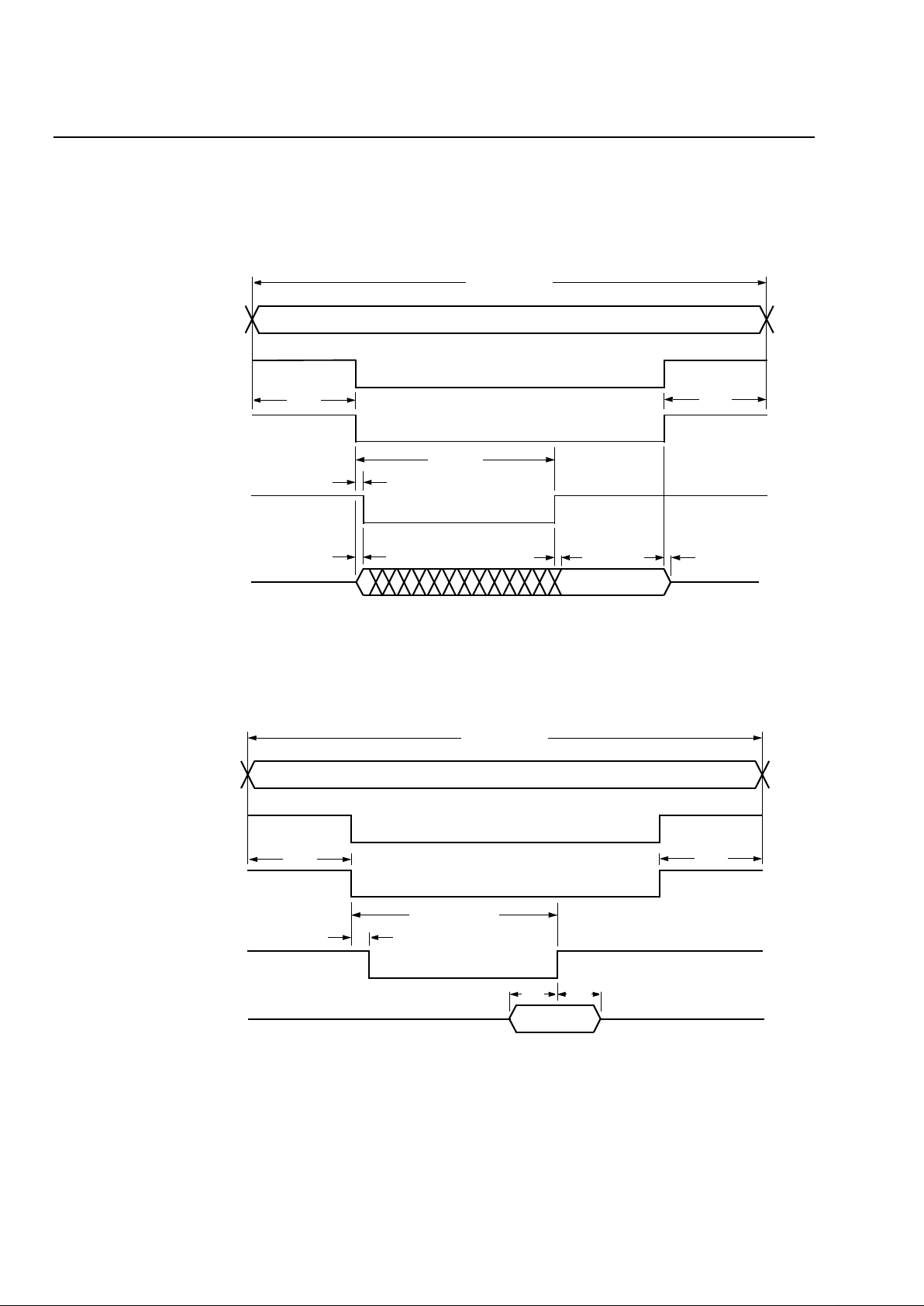
42 Agere Systems Inc.
Data Sheet
May 2001
and Packet Payload Engine
Ambassador
T8110 PCI-Based H.100/H.110 Switch
5 Microprocessor Interface (continued)
5-9419 (F)
Figure 17. Microprocessor Access Timing,
Intel
Protocol
ADDRESS VALID
tah
tRDYhi
tas
taccess
WORD/BYTE SELECT,
A[19:0]
CSn
WRn
D[15:0], WRITE CYCLE
WR DATA
VALID
tds tdh
RDY
tRDYlo
Microprocessor Access Write Cycle,
Intel
Protocol
ADDRESS VALID
tah
tRDYhi
tas
taccess
WORD/BYTE SELECT,
A[19:0]
CSn
DSn
RDY
tRDYlo
tdz
READ DATA VALID
D[15:0 ],
tde td v
READ CYCLE
Microprocessor Access Read Cycl e,
Intel
Protocol
5-9418 (F)

Agere Systems Inc. 43
Data Sheet
May 2001
and Packet Payload Engine
Ambassador
T8110 PCI-Based H.100/H.110 Switch
5 Microprocessor Interface (continu ed)
5-9417 (F)
Figure 18. Microprocesso r Access Timing,
Motorola
Protocol
ADDRESS VALID
tah
tDTACKhi
tDTACKlo
tde tdv
tdz
tas
READ DATA VALID
taccess
WORD/BYTE SELECT,
A[19:0]
R/Wn
CSn
DSn
DTACKn
D[15:0], READ CYCLE
5-9416 (F)
Microprocessor Access Read Cycle,
Motorola
Protocol
ADDRESS VALID
tah
tDTACKhi
tDTACKlo
tas
taccess
WORD/BYTE SELECT,
A[19:0]
R/Wn
CSn
DSn
DTACKn
D[15:0], WRITE CYCLE
WR DATA
VALID
tds tdh
Microprocessor Access Write Cycle,
Motorola
Protocol

44 Agere Systems Inc.
Data Sheet
May 2001
and Packet Payload Engine
Ambassador
T8110 PCI-Based H.100/H.110 Switch
5 Microprocessor Interface (continued)
5.3.2 Register Space Access
The T8110 registers are always immediately available for access, providing low latency time to acknowledge the
transaction. Read access to [reserved] addresses returns 0x00. Register access timing for Figure 17 and Figure 18
is shown below.
5.3.3 Connection Memory Space Access
The T8110 connection memory is always immediately availa ble for access (via dedicated acces s times assigne d
for microprocessor transactions) providing low latency time to acknowledge the transaction. Connection memory
access timing for Figure 17 and Figure 18 is shown below.
Table 17. Register Space Acces s Timing
Name Parameter Min (ns) Max (ns)
taccess Overall Access Time 41 —
tas Address Setup Time 5 —
tah Address Hold Time 0 —
tRDYlo
Intel
Cycle, Time to RDY Deasserte d 6 12
tRDYhi
Intel
Cycle, Time to RDY Reasserted 36 72
tDTACKlo
Motorola
Cycle, Time to DT ACKn Asserted 36 70
tDTACKhi
Motorola
Cycle, Time to DTACKn Deasserted 10 15
tde Read Cycle, Time to Data Enabled 7 14
tdv Read Cycle, Time to Data Valid 5 9
tdz Read Cycle, Time to Data Invalid 10 16
tds Write Cycle, Data Setup Time 25 —
tdh Write Cycle, Data Hold Time 0 —
T able 18. Connection Memory Space Access Timing
Name Parameter Min (ns) Max (ns)
taccess Overall Access Time 41 —
tas Address Setup Time 5 —
tah Address Hold Time 0 —
tRDYlo
Intel
Cycle, Time to RDY Deasserte d 6 12
tRDYhi
Intel
Cycle, Time to RDY Reasserted 36 72
tDTACKlo
Motorola
Cycle, Time to DTACKn Asserted 36 70
tDTACKhi
Motorola
Cycle, Time to DTACKn Deasserted 10 15
tde Read Cycle, Time to Data Enabled 7 14
tdv Read Cycle, Time to Data Valid 5 9
tdz Read Cycle, Time to Data Invalid 10 16
tds Write Cycle, Data Setup Time 25 —
tdh Write Cycle, Data Hold Time 0 —

Agere Systems Inc. 45
Data Sheet
May 2001
and Packet Payload Engine
Ambassador
T8110 PCI-Based H.100/H.110 Switch
5 Microprocessor Interface (continu ed)
5.3.4 Data Memory Space Access
The T8110 data memory is not guaranteed to be immediately available for access. Access to data memory is prioritized for standard H-bus/L-bus switching, with microprocessor bus transaction access allowed as the lowest priority. The latency time to acknowledge these transactions is indeterminate and depen ds on the H-bus/L-bus
switching configuration. Data memory access timing for Figure 17 and Figure 18 is shown below.
* Max data memory space access time is indeterminate, and depends on how much of the data memory access bandwidth is being taken by
TDM switch connections.
5.3.5 Virtual Channel Memory Space Access
Microprocessor access to the virtual channel memory is provided for diagnostic purposes only and is disabled by
default. Access to this region is enabled via the diagnostic registers; see Section 13 on page 128. The T8110 virtual channel memory is not guaranteed to be immediately available for access. Access to virtual channel memory
is prioritized for standard H-bus/L-bus switching, with microprocessor bus transaction access allowed as the lowest priority . The latency time to acknowledge these transactions is indeterminate and depends on the H-bus/L-bus
switching configuration. Virtual channel memory access timing for Figure 17 and Figure 18 is shown below.
* Immediate response, same as register access, assuming no virtual channe l connections are programmed into the connection memory (virtual
channels aren’t supported with the microprocessor interface protocol selected).
Table 19. Data Memory Space Access Timing
Name Parameter Min (ns) Max (ns)
taccess Overall Access Time 4 1 *
tas Address Setup Time 5 —
tah Address Hold Time 0 —
tRDYlo
Intel
Cycle, Ti me to RDY Deasserted 6 12
tRDYhi
Intel
Cycle, Ti me to RDY Reasserted 36 *
tDTACKlo
Motorola
Cycle, Time to DTACKn Asserted 36 *
tDTACKhi
Motorola
Cycle, Time to DTACKn Deasserted 10 15
tde Read Cyc le, Time to Data Enabled 7 14
tdv Read Cycle, Time to Data Valid 5 9
tdz Read Cycle, Time to Data Invalid 10 16
tds Write Cycle, Data Setup Time 25 —
tdh Write Cycle, Data Hold Time 0 —
T able 20. Virtual Channel Memory Space Access Timing
Name Parameter Min (ns) Max (ns)
taccess Overall Access Time 41 —
tas Address Setup Time 5 —
tah Address Hold Time 0 —
tRDYlo
Intel
Cycle, Time to RDY Deasserted 6 1 2
tRDYhi
Intel
Cycle, Time to RDY Reasserted 36 57*
tDTACKlo
Motorola
Cycle, Time to DTACKn Asserted 36 55*
tDTACKhi
Motorola
Cycle, Time to DTACKn Deasserted 10 15
tde Read Cycle, Time to Data Enabled 7 1 4
tdv Read Cycle, Time to Data Valid 5 9
tdz Read Cycle, Time to Data Invalid 10 16
tds Write Cycle, Data Setup Time 25 —
tdh Write Cycle, Data Hold Time 0 —

46 Agere Systems Inc.
Data Sheet
May 2001
and Packet Payload Engine
Ambassador
T8110 PCI-Based H.100/H.110 Switch
6 Operating Control and Status
Overall T8110 operational control and status is configured via registers occupying 0x00100—0x001FC in the
address space.
6.1 Control Registers
General control functions are soft reset, reset configuration, overall master output enables, and data memory configuration. Clocking-specific general control functions are clock register access configuration, phase alignment,
clock fallback, and clock watchdog configuration.
* VCSTART and external buffers descriptor table registers are only relevant if the T8110 interfaces to the PCI bus. If the selected T8110
interface is to the microprocessor bus, this register is [reserved].
6.1.1 Reset Registers
The soft reset and reset select registers control soft reset functions and reset signal masking. Writes to the soft
reset register trigger the corresponding action, and the set bit(s) are automatically cleared.
n
Power-on reset: nonmaskable:
— At power-on, initialize all T8110 registers (including reset select register) and connection valid flags, and ini-
tialize the T8110 PCI interface. The power-on reset cell test input i s controlled vi a diagnostic register; see Section 13.
n
Hard reset: maskable via reset select r e gister, H RBEB:
— On assertion of RESET#, initialize all T8110 registers (excluding reset select register) and connection valid
flags.
n
PCI reset: nonmaskable to PCI interface:
— Maskable to T8110 back-end via reset select register, PRBEB.
On assertion of PCI_RST#, initialize the T8110 PCI interface. If unmasked (PRBEB = 1), also initialize all
T8110 registers (excluding reset select register) and connection valid flags.
— Maskable to minibridge port via reset select register, PMBEB.
The PCI_RST# input to the T8110 can be forwarded to the minibridge port, using the GP(2) output (via register 0x00503; see Section 9.1 on page 98). Polarity of the forwarded reset is selectable (via register 0x00781;
see Section 11.2 on page 110).
Soft resets are maskable via reset select register, SRBEB, and selectable via soft reset register, SRESR.
n
Soft reset 1: Initialize all T8110 registers (excluding reset select register) and connection valid flags.
n
Soft reset 2: Initialize all T8110 registers (excluding reset select register).
n
Soft reset 3: Reset all interrupt pending registers and the interrupt in-service register.
Table 21. Control Register Map
DWORD
Address
(20 bits)
Register
Byte 3 Byte 2 Byte 1 Byte 0
0x00100 M as ter enable Reserved R eset select Soft reset
0x00104 Phase alignment select Clock register access
select
Data memory mode select VCSTART*
0x00108 Fallback trigger, upper Fallback trigger, lower Fallback type select Fallback control
0x0010C W atchdog EN, upper Watchdog EN, lower Watchdog select,
NETREF
Watchdog select, C8
0x00110 External buffers descriptor table—base address register [31:0]*
0x00114 Reserved Failsafe threshold low Failsafe enable and status Failsafe control

Agere Systems Inc. 47
Data Sheet
May 2001
and Packet Payload Engine
Ambassador
T8110 PCI-Based H.100/H.110 Switch
6 Operating Control and Status (continued)
n
Soft reset 4: Reset the interrupt in-service register only.
n
RESET_PENDING_MEM: Reset the virtual channel NOTIFY_PENDING memory.
n
RESET_QUEUE: Reset the virtual channel NOTIFY_QUEUE FIFO.
6.1.2 Master Output Enable Register
The master output enable register is used to control master output enables to various groups of T8110 signals,
including the following:
L-bus data streams (L_D[31:0])
L-bus clocks (L_SC[3:0], FG[7:0] when used as frame group outputs)
H-bus data streams (CT_D[31:0])
H-bus clocks (CT_C8_A, /CT_FRAME_A, CT_C8_B, /CT_FRAME_B, CT_NETREF1,CT_NET REF2, /C16+,
/C16–, /C4, C2, SCLK, /SCLKx2, /FR_COMP)
GPIO (GP[7:0])
FGIO (FG[7:0] when used as programmable register outputs)
Minibridge (MB_A[15:0], MB_CS[7:0], MB_RD, MB_WR, MB_D[15:0] )
T8110 outputs that are not programmatically enabled (i.e., always driven except during reset) include the following:
CLKERR, SYSERR, PRI_REF_OUT, NR1_SEL_OUT, and NR2_SE L_OUT.
Table 22. Reset Registers
Byte
Address
Name Bit(s) Mnemonic Value Function
0x00100 Soft Reset 7:0 SRES R 0000 0000
0000 0001
0000 0010
0001 0000
0010 0000
0100 0000
1000 0000
NOP (default value).
Reset all registers and connection valid flags.
Reset all registers.
Reset interrupt pending and in-service registers.
Reset interrupt in-service register only.
Reset virtual channel NOTIFY_PENDING memory.
Reset virtual channel NOTIFY_QUEUE.
0x00101 Reset Select 7:4 Reserved 0000 NOP (default).
3PMBEB 01Disable PCI reset to minibridge (default).
Enable PCI reset to minibridge.
2PRBEB 01Disable PCI reset to back end (default).
Enable PCI reset to back end.
1 HRBEB 0
1
Disable hard reset to back end.
Enable hard reset to back end (default).
0SRBEB 01Disable soft resets to back end.
Enable soft resets to back end (default).

48 Agere Systems Inc.
Data Sheet
May 2001
and Packet Payload Engine
Ambassador
T8110 PCI-Based H.100/H.110 Switch
6 Operating Control and Status (continued)
*MBREB is only relevant if the T8110 interfaces to t he PCI bus. If the se lected T 8110 interface is to the microprocessor bus, this bit is reserved.
6.1.3 Connection Control—Virtual Channel Enable and Data Memory Selector Register
The VC start register is used as an overall enable/disable for virtual channel switching activity, with the option to
synchronize the enabling of switching activity with the internal 8 kHz frame reference (refer to Section 14.2.3 for
more detail). Writes to the VC start register trigger the corresponding action, and the set bit(s) are automatically
cleared.
The data memory mode select register MSbit controls subrate switching enable. The lower 7 bits control the T8110
data memory switching configuration. For more details, see Section 14.2.1.2 on page 148.
There are six data memory configurations as outlined below. (If the T8110 interfac es to the PCI bus, all configurations are valid. If the interface selection is to the microprocessor bus, only the standard switching configurations
1—3 are allowed.)
Table 23. Master Output Enable Register
Byte
Address
Name Bit(s) Mnemonic Value Function
0x00103 Master Enable 7 AIOEB 0
1
Individual enables via bits [6:0] (default).
E nabl e all (same as bits [6: 0] = 1111111).
6MBREB 01Disable minibridge* (default).
Enable minibridge.
Note: If AIOEB is set to 1 to enable all then
MBREB must also be set to 1 to enable the
minibridge.
5FGREB 01Disable FGIO (default).
Enable FGIO.
4GPIEB 01Disable GPIO (default).
Enable GPIO.
3 HCKEB 0
1
Disable H-bus clocks (default).
Enable H-bus clocks.
2 HDBEB 0
1
Disable H-bus data streams (default).
Enable H-bus data streams.
1LCKEB 01Disable L-bus clocks, L_SC, FG (default).
Enable L-bus clocks.
0LDBEB 01Disable L-bus data streams (default).
Enable L-b us data streams .
Table 24. Virtual Channel Enable and Data Memory Selector Register
Byte
Address
Name Bit(s) Mnemonic V alue Function
0x00104 VCSTART 7:0 VCSSR 0000 0000
0001 0001
0000 0010
0000 0001
0001 0010
NOP (default).
START (enable) VC switching, immediate.
PAUSE (disable) VC switching, immediate.
START VC switching, synchronized to frame.
PAUSE VC switching, synchronize d to frame.

Agere Systems Inc. 49
Data Sheet
May 2001
and Packet Payload Engine
Ambassador
T8110 PCI-Based H.100/H.110 Switch
6 Operating Control and Status (continued)
1. 4k single-buffered switch. Standard H-bus/L-bus switching only, up to 4096 simplex connections, all connections
are minimum delay due to single-buffer configuration.
2. 2k double-buffered switch. Standard H-bus/L-bus switching only, up to 2048 simplex connections, all connections are programmable for minimum or constant delay via the double-buffer configuration.
3. 2k single-buffered switch + 1k double-buffered switch. Standard H-bus/L-bus switching only, up to 2048 simplex
minimum delay connections (single buffer) and up to 1024 simplex minimum or constant delay connections
(double buffer).
4. 2k single-buffered switch + 256 virtual channels. Standard H-bus/L-bus switching, up to 2048 simplex minimum
delay connections (single buffer), PLUS packet payload switching, up to 256 virtual channels.
5. 1k double-buffered switch + 256 virtual channels. Standard H-bus/L-bus switching, up to 1024 simplex minimum
or constant delay connections (double buffer), PLUS packet payload switching, up to 256 virtual
channels.
6. No standard switching + 512 virtual channels. Packet payload switching only, up to 512 virtual channels.
6.1.4 General Clock Control (Phase Alignment, Fallback, Watchdogs) Register
The clock regi ste r a ccess select register controls the selection between accessing the active vs. the inactive set of
T8110 clock registers. The T81 10 contains two sets of clock registers, X and Y. The X and Y register sets are comprised of the registers listed in Table 43 on page 63, Clock Input Control Register Map, and Table 56 on page 72,
Clock Output Control Register Map. Only one set is used at a time. It is selected based on the clock fallback setup.
The clock register set that is currently in use is denoted as the active set; see Section 7.3 on page 76 for more
details.
T a ble 25. Data Memory Mode Select Register
Byte
Address
Name Bit(s) Mnemonic Value Function
0x00105 Dat a Memory Mod e
Select
7 GSREB 0
1
Disable subrate switching (default).
Enable subrate switching.
6:0 DMMSP 100 0000
010 0000
011 0000
010 0010
001 0010
000 0100
4k single-buffer switch (default).
2k double-buffer switch.
2k single-buffer, 1k double-buffer switch.
2k single buffer switch, 256 virtual channels.
1k double buffer switch, 256 virtual channels.
512 virtual channels.
Table 26. Clock Register Access Select Register
Byte
Address
Name Bit(s) Mnemonic Value Function
0x00106 Clock Register Access
Select
7:0 CSASR 0000 0000
0000 0001
Access inactive clock registers (default).
Access active clock registers.

50 Agere Systems Inc.
Data Sheet
May 2001
and Packet Payload Engine
Ambassador
T8110 PCI-Based H.100/H.110 Switch
6 Operating Control and Status (continued)
6.1.5 Phase Alignment Select Register
The phase alignment select register selects the phase alignment configuration. For more details, see Section
7.4.5.1 on page 80. The T8110 internally generates an 8 kHz frame reference. Shown below are three configurations to control phase alignment between this internally generated frame reference and a selected incoming frame
reference from the H-bus (/CT_FRAME_A, /CT_FRAME_B, or /FR_COMP) or local clock reference (LREF[4:7]).
n
Disable alignment, no realignment of unaligned frames
n
Snap alignment , immediate realignment of unaligned fra mes
n
Slide alignment, gradual realignment of unaligned frames
6.1.6 Fallback Control Register
The fallback control register allows user control over the active and inactive clock register sets. For more details,
see Section 7.7.1 on page 82. Writes to the fallback control register trigger the corresponding action, and the set
bit(s) are automatically cleared. The four commands are shown below:
n
GO_CLOCKS. At initialization, the clock register Y set is active, the X set is inactive, and access is enabled to
the X set. The GO_CLOCKS command transitions the Y set to inactive and the X set to active. This command
can either be performed immediately upon issue or can wait to be performed until the next 8 kHz frame reference
(synchronized to frame).
n
CLEAR_FALLBACK. Forces a state transition for active/inactive assignment of the clock register X and Y sets
after a fallback event has occurred. This command can either be performed immediately upon issue or can wait
to be performed until the next 8 kHz frame reference (synchronized to frame).
n
FORCE_FALLBACK. Forces a state transition for active/inactive assignment of the clock register X and Y sets
by creating a fallback event. This command can either be performed immediately upon issue or can wait to be
performed until the next 8 kHz frame reference (synchronized to frame).
n
COPY ACTIVE TO INACTIVE SET. Copies all register values in the current active clock register set to the inactive clock register set. This command is performed immediately upon issue.
Table 27. Phase Alignment Select Register
Byte
Address
Name Bit( s ) Mnem onic Value Function
0x00107 Phase Alignment Select 7:0 PAFSR 0000 0000
0000 0001
0000 0010
Phase alignment is disabled (default).
Enable snap alignment.
Enable slide alignment.

Agere Systems Inc. 51
Data Sheet
May 2001
and Packet Payload Engine
Ambassador
T8110 PCI-Based H.100/H.110 Switch
6 Operating Control and Status (continued)
* The sy nchroni z ed to frame command also has a diagnostic element—instead of perf orming th e command ri ght at the frame boundary,
the use r can elect to perfo rm the command at a specified o ffset t ime from the frame boundary, by programming the Diag11 and Diag10
registers, 0x0014B—0x0014A.
6.1.7 Fallback Type Select Register
The upper nibble configures which H-bus clocks are selected to trigger a clock fallback event. Any of the legacy
modes have predetermined trigger enables and ignore the fallback trigger register settings. Nonleg acy modes
require the fallback trigger register settings. For more details, see Section 7.7.1 on page 82.
The lower nibble configures the state machine that controls clock register set active/inactive assignments. There
are three possible selections. For more details, see Section 7.7 on page 82.
n
Disabled. No transitions of clock register X and Y sets to active/inactive.
n
Fixed secondary. Swap the active/inactive sets on a fallback event; swap them back when fallback is cleared.
n
Rotating secondary. Swap the active/inactive sets on a fallback event; maintain this state when fallback is
cleared.
6.1.8 Fallback Trigg er Register s
The fallback trigger registers are used in conjunction with the fallback type select register and control which H-bus
clocks are enabled to trigger a clock fallback event in case of error. The sync reference inputs to DPLL1 and
DPLL2 can also trigger a clock fallback event upon detection of an error.
Table 28. Fallback Control Register
Byte
Address
Name Bit(s) Mnemo nic Value Function
0x00108 Fallback Control 7:0 FBCSR 0000 0000
0000 0001
0000 0010
0000 0100
0001 0001
0001 0010
0001 0100
0010 0000
NOP (default).
GO_CLOCKS command.
CLEAR_FALLBACK command.
FORCE_FALLBACK command.
GO_CLOCKS synchronized to frame*.
CLEAR_FALLBACK synchronized to frame*.
FORCE_FALLBACK synchronized to frame*.
COPY ACTIVE TO INACTIVE SET command.
Table 29. Fallback Type Select Register
Byte
Address
Name Bit(s) Mn e m onic Value Function
0x00109 F all back Type
Select
7:4 FTRSN 0 000
0001
0010
0100
1000
1001
NOP (default).
Legacy, fallback to OSC/4 on main select failure.
Legacy, fallback X/Y set on main select failure.
Legacy, fallback X/Y set on H-bus A/B failure.
Fallback trigger registers control fallback.
Fallback trigger registers control fallback and
H-Bus clock enable state machine is enabled.
3:0 FSMSN 0000
0001
0010
Fallback is disabled (default).
Enable fixed secondary fallback.
Enable rotating secondary fallback.

52 Agere Systems Inc.
Data Sheet
May 2001
and Packet Payload Engine
Ambassador
T8110 PCI-Based H.100/H.110 Switch
6 Operating Control and Status (continued)
6.1.9 Watchdog Select, C8, and NETREF Registers
The watchdog select, C8 register controls the watchdog circuits to monitor the proper frequency for the CT_C8_A
and CT_C8_B signals. These signals can take on two values, including 8.192 MHz (ECTF mode) and 4.096 MHz
(MC1 mode).
The watchdog select, NETREF register controls the watchdog circuits to monitor the proper frequency for the
CT_NETREF1 and CT_NETREF2 signals. These signals can take on three values depending on system-level
clocking architecture, including 8 kHz (frame reference), 1.544 MHz (T1 bit clock), and 2.048 MHz (E1 bit clock).
Table 30. Fallback Trigger Registers
Byte
Address
Name Bit(s) Mnemo nic Value Functio n
0x0010A Fallback Trigger, Lower 7 S2FEB 01Disable /SCLKx2 trigger (default).
Enable /SCLKx2 trigger.
6SCFEB01Disable SCLK trigger (default).
Enable SCLK trigger.
5C2FEB01Disable C2 trigger (default).
Enable C2 trigger .
4C4FEB01Disable /C4 trigger (default).
Enable /C4 trigger .
3CMFEB01Disable /C16– trigger (default).
Enable /C16– trigger.
2CPFEB01Disable /C16+ trigger (default).
Enable /C16+ trigger.
1CBFEB01Disable CT_C8_B trigger (default).
Enable CT_C8_B trigger.
0CAFEB01Disable CT_C8_A trigger (default).
Enable CT_C8_A trigger.
0x0010B Fallback Trigger, Upper 7 Reserved 0 NOP (default).
6D2FEB01Disable DPLL2 sync trigger (default).
Enable DPLL2 sync trigger.
5D1FEB01Disable DPLL1 sync trigger (default).
Enable DPLL1 sync trigger.
4N2FEB01Disable CT_NETREF2 trigger (default).
Enable CT_NETREF2 trigger.
3N1FEB01Disable CT_NETREF1 trigger (default).
Enable CT_NETREF1 trigger.
2FCFEB01Disable /FR_COMP trigger (default).
Enable /FR_COMP trigger.
1FBFEB01Disable /CT_FRAME_ B trigger (default).
Enable /CT_FRAME_B trigger.
0 FAFEB 01Disable /CT_FRAME_ A trigger (default).
Enable /CT_FRAME_A trigger.

Agere Systems Inc. 53
Data Sheet
May 2001
and Packet Payload Engine
Ambassador
T8110 PCI-Based H.100/H.110 Switch
6 Operating Control and Status (continued)
6.1.10 Watchdog EN Register
The watchdog EN registers are used to enable/disable watchdogs on the individual H-bus clocks and the watchdogs on the sync inputs of DPLL1 and DPLL2.
T able 31. Watchdog Select, C8, NETREF Registers
Byte
Address
Name Bit(s) Mnemonic Value Function
0x0010C Watchdog Select, C8 7:4 CBWSN 0000
0001
CT_C8_B watchdog at 8.192 MHz (default).
CT_C8_B watchdog at 4.096 MHz MC1mode.
3:0 CAWSN 0000
0001
CT_C8_A watchdog at 8.192 MHz (default).
CT_C8_A watchdog at 4.096 MHz MC1mode.
0x0010D Watchdog Select,
NETREF
7:4 N2WSN 0000
0001
0010
CT_NETREF2 watchdog at 8 kHz (default).
CT_NETREF2 watchdog at 1.544 MHz.
CT_NETREF2 watchdog at 2.048 MHz.
3:0 N1WSN 0000
0001
0010
CT_NETREF1 watchdog at 8 kHz (default).
CT_NETREF1 watchdog at 1.544 MHz.
CT_NETREF1 watchdog at 2.048 MHz.
T able 32. Watchdog EN Registers
Byte
Address
Name Bit(s) Mnemonic Value Function
0x0010E Watchdog EN, Lower 7 S2WEB 01Disable /SCLKx2 watchdog (default).
Enable /SCLKx2 watchdog.
6SCWEB 01Disable SCLK watchdog (default).
Enable SCLK watchdog.
5C2WEB 01Disable C2 watchdog (default).
Enable C2 watchdog.
4C4WEB 01Disable/C4 watchdog (default).
Enable/C4 watchdog.
3CMWEB 01Disable/C16– watchdog (default).
Enable/C16– watchdog.
2 CPWEB 01Disable/C16+ watchdog (default).
Enable/C16+ watchdog.
1 CBWEB 01Disable CT_C8_B watchdog (default).
Enable CT_C8_B watchdog.
0CAWEB 01Disable CT_C8_A watchdog (default).
Enable CT_C8_A watchdog.

54 Agere Systems Inc.
Data Sheet
May 2001
and Packet Payload Engine
Ambassador
T8110 PCI-Based H.100/H.110 Switch
6 Operating Control and Status (continued)
6.1.11 Failsafe Control Registers
The failsafe control register controls a return from the failsafe state. Writes to the failsafe control register trigger the
corresponding action, and the set bit(s) are automatically cleared. From the failsafe state, the user can return to
either the primary or secondary clock register sets. For more on failsafe, please see Section 7.7.2 on page 88.
Byte
Address
Name Bit(s) Mnemonic Value Function
0x0010F Watchdog EN, Upper 7 FS WE B 01Disable FAILSAFE ref watchdog (default).
Enable FAILSAFE ref watchdog.
6D2WEB 01Disable DPLL2 sync watchdog (default).
Enable DPLL2 sync watchdog.
5D1WEB 01Disable DPLL1 sync watchdog (default).
Enable DPLL1 sync watchdog.
4N2WEB 01Disable CT_NETREF2 watchdog (default).
Enable CT_NETREF2 watchdog.
3N1WEB 01Disable CT_NETREF1 watchdog (default).
Enable CT_NETREF1 watchdog.
2FCWEB 01Disable /FR_COMP watchdog (default).
Enable /FR_COMP watchdog.
1 FBWEB 01Disable /CT_FRAME_B watchdog (default).
Enable /CT_FRAME_B watchdog.
0FAWEB 01Disable /CT_FRAME_A watchdog (default).
Enable /CT_FRAME_A watchdog.
Table 33. Failsafe Control Register
Byte
Address
Name Bit(s) Mnemonic Value Function
0x00114 Failsafe Control 7:0 FSCSR 0000 0000
0000 0001
0000 0010
NOP (default).
Return from failsafe to nonfallback condition.
Return from failsafe to fallback condition.
0x00115 Failsafe Enable 7:0 FSEER 0000 0000
0000 0001
Failsafe disabled.
Failsafe enabled.
0x00116 Failsafe Sensitivity 7:0 FSSSR 0000 0000
0000 0001
0000 0010
0000 0100
0000 1000
Failsafe watchdog highest sensitivity .
Failsafe watchdog + 30.5 ns.
Failsafe watchdog + 121.0 ns.
Failsafe watchdog + 244.0 ns.
Failsafe watchdog + 488.0 ns.
0x00118 OOL Threshold Low 7 :0 OLLLR LLLL LLLL Failsafe threshold value, low byte.
0x00119 OOL Threshold High 7 :0 OLHLR LLLL LLLL Failsafe threshold value, high byte.
0x0011A OOL Monit or 7:0 OOLER 0000 000 0
0000 0001
Monitor direct APLL1 lock detect at PLOCK.
Monitor user threshold lock detect at PLOCK.
Table 32. Wa tchdog EN R egisters (continued)

Agere Systems Inc. 55
Data Sheet
May 2001
and Packet Payload Engine
Ambassador
T8110 PCI-Based H.100/H.110 Switch
6 Operating Control and Status (continued)
The failsafe enable register controls the enable/disable of failsafe operation. For more on failsafe operation, please
see Section 7.7.2 on page 88.
The failsafe sensitivity register allows the failsafe watchdog timer to be desensitized by either 1, 4, 8, or 16 watchdog sample clock periods.
The OOL threshold registers allow for programmable threshold times which indicate the APLL1 out-of-lock. Resolution for the threshold value increments is one 32.768 MHz clock period (30.5 ns). The register contains
[count – 1], a value of 0x0000 yields a 30.5 ns threshold. A value of 0xFFFF yields a 1.99 ms threshold. For more
on OOL operation, please see Section 7.7.2 on page 88.
The OOL monitor register allows the user to monitor either the raw APLL1 out-of-lock status, OR the status flag
that indicates that the APLL1 has been out-of-lock for more than the threshold defined in the OOL threshold registers.
6.1.12 External Buffers—Descriptor Table Base Address
* The external buffers descriptor table base address is only relevant if the T8110 interfaces to the PCI bus. If the selected T8110 in te rf ace
is to the microprocessor bus, this register is reserved. For more details, refer to Section 14.2.3.4 on page 160.
6.2 Error and Status Registers
Status 7, 6, and 3—0 registers are writable by the user for clearing specific error bits. Writing a 1 to any of the bits
of these registers will clear the corresponding error bit. The remaining error and status registers are read-only.
Table 34. Extended Buffers Base Addresses
Byte
Address
Name Bit(s) Mnemonic Value Function
0x00110 Base Address Byte 0 7:0 NA LLLL LLLL 32-bit base address value for external
buffers descriptor table*.
0x00111 Base Address Byte 1 7:0 NA LLLL LLLL 32-bit base address value for external
buffers descriptor table*.
0x00112 Base Address Byte 2 7:0 NA LLLL LLLL 32-bit base address value for external
buffers descriptor table*.
0x00113 Base Address Byte 3 7:0 NA LLLL LLLL 32-bit base address value for external
buffers descriptor table*.
Table 35. Error and Status Register Ma p
DWORD
Address
(20 bits)
Register
Byte 3 Byte 2 Byte 1 Byte 0
0x00120 Status 3, latched
clock errors, upper
Status 2, latched
clock errors, lower
Status 1, transient clock
errors, upper
Status 0, transient
clock errors, lower
0x00124 Status 7, system
errors, upper
Status 6, system
errors, lower
Status 5 PLL and switching
status
Status 4 fallback and
failsafe status
0x00128 Device ID, upper Device ID, lower Reserved Version ID
0x0012C Reserved Reserved Status 9, virtual channel
status
Status 8, PCI target
queue status

56 Agere Systems Inc.
Data Sheet
May 2001
and Packet Payload Engine
Ambassador
T8110 PCI-Based H.100/H.110 Switch
6 Operating Control and Status (continued)
6.2.1 Clock Errors
6.2.1.1 Transient Clock Errors Registers
The transient clock error registers are used in conjunction with the watchdog EN registers and indicate error status
for H-bus clocks and DPLL1/DPLL2 sync inputs whose watchdogs are enabled. The transient indicators are
dynamic in nature; if a clock is in error only for a short time and then recovers, the error indication is deasserted
when the clock recovers. Additionally, an APLL1 out-of-lock indicator is provided, and used in conjunction with the
failsafe clocking mode. For more details, please see Section 7.7.1 on page 82 and Section 7.7.2 on page 88.
T able 36. Clock Error Registers
Byte Address Name Bit(s) Mnemonic Value Function
0x00120 Status 0, Transient
Clock Errors, Lower
7S2TOB01/SCLKx2 no error (default).
/SCLKx2 error.
6SCTOB01SCLK no error (default).
SCLK error.
5C2TOB01C2 no error (default).
C2 error.
4C4TOB01/C4 no error (default).
/C4 error.
3CMTOB 01/C16– no error (default).
/C16– error.
2CPTOB 01/C16+ no error (default).
/C16+ error.
1CBTOB01CT_C8_B no error (default).
CT_C8_B error.
0CATOB 01CT_C8_A no error (default).
CT_C8_A error.
0x00121 Status 1, Transient
Clock Errors, Upper
7FSTOB01Failsafe indicator: APLL1 reference no error.
APLL1 reference error.
6D2TOB01DPLL2 sync no error (default).
DPLL2 sync error.
5D1TOB 01DPLL1 sync no error (default).
DPLL1 sync error.
4N2TOB01CT_NETREF2 no error (default).
CT_NETREF2 error.
3N1TOB 01CT_NETREF1 no error (default).
CT_NETREF1 error.
2FCTOB01/FR_COMP no error (default).
/FR_COMP error.
1FBTOB01/CT_FRAME_B no error (default).
/CT_FRAME_B err or.
0FATOB 01/CT_FRAME_A no error (default).
/CT_FRAME_A err or.

Agere Systems Inc. 57
Data Sheet
May 2001
and Packet Payload Engine
Ambassador
T8110 PCI-Based H.100/H.110 Switch
6 Operating Control and Status (continued)
6.2.1.2 Latched Clock Error Register
The latched clock error registers capture transient clock errors. The latched indicators capture and hold any transient error status and are used by the clock fallback logic. For more details, see Section 7.7 on page 82, and Section 12 on page 113 for more details.
T able 37. Latched Clock Error Registers
Byte
Address
Name Bit(s) Mnemonic Value Function
0x00122 Status 2, Latched Clock
Errors, Lowe r
7S2LOB01/SCLKx2 no error (default).
/SCLKx2 error.
6SCLOB01SCLK no error (default).
SCLK error.
5 C2LOB 01C2 no error (default).
C2 error.
4 C4LOB 01/C4 no error (default).
/C4 error.
3CMLOB01/C16– no error (default).
/C16– error.
2CPLOB01/C16+ no error (default).
/C16+ error.
1CBLOB01CT_C8_B no error (default).
CT_C8_B error.
0CALOB01CT_C8_A no error (default).
CT_C8_A error.
0x00123 Status 3, Latched Clock
Errors, Upper
7FSLOB01Failsafe indicator: APLL1 reference no error .
APLL1 reference error.
6 D2LOB 01DPLL2 sync no error (default).
DPLL2 sync error.
5 D1LOB 01DPLL1 sync no error (default).
DPLL1 sync error.
4 N2LOB 01CT_NETREF2 no error (default).
CT_NETREF2 error.
3 N1LOB 01CT_NETREF1 no error (default).
CT_NETREF1 error.
2FCLOB01/FR_COMP no error (default).
/FR_COMP error.
1FBLOB01/CT_FRAME_B no error (default).
/CT_FRAME_B error.
0FALOB01/CT_FRAME_A no error (default).
/CT_FRAME_A error.

58 Agere Systems Inc.
Data Sheet
May 2001
and Packet Payload Engine
Ambassador
T8110 PCI-Based H.100/H.110 Switch
6 Operating Control and Status (continued)
6.2.2 System Status
6.2.3 Clock Fallback Status Register
The upper nibble provides status indicators for clock fallback. FBFOB indicates whether the circuit is in a clock fallback state. FBSOP indicates which of five possible states the circuit is in; see Section 7.7.1 on page 82 for more
details.
The lower nibble provides status indicators related to the X and Y clock register set active/inactive assignments.
XYSOB indicates which of the clock register sets is active. The remaining bits indicate a pending status for
GO_CLOCKS, CLEAR_FALLBACK, and FORCE_FALLBACK commands issued (via the fallback control register,
0x00108), which are waiting for a frame sync.
.
6.2.4 PLL and Switching Status Register
The upper 6 bits provide APLL1, DPLL1, and DPLL2 lock status. For more details, see Section 7 on page 62. The
lower 2 bits provide memory status as follows: CMROB is an indicator for the connection memory actively resetting; see Section 14.2.1.1 on page 146. DMPOB indicates the active data page used for double-buffered standard
switching; see Section 14.2.1.2 on page 148.
Table 38. Fallback and Failsafe Status Register
Byte
Address
Register Name Bit(s) Mne monic Value Function
0x00124 S tatus 4, Clock Fallback
Status
7FBFOB01Indicates not in fallback/failsafe state (default).
Indicates fallback/failsafe state.
6:4 FBSOP 111
000
001
010
01 1
100
101
Fallback state = INITIAL (default).
Fallback state = PRIMARY.
Fallback state = TO_PRIMARY.
Fallback state = SECONDARY.
Fallback state = TO_SECONDARY.
Failsafe state = FS_1.
Failsafe state = FS_2.
3 XYSOB 01Clock register Y set is active, X is inactive.
Clock register X set is active, Y is inactive.
2GOPOB01No GO_CLOCKS pending (default).
GO_CLOCKS pending, waiting for frame.
1CFPOB01No CLEAR_FALLBACK pending (default).
CLEAR_FALLBACK pending, waiting for frame.
0FFPOB01No FORCE_FALLBACK pending (default).
FORCE_FALLBACK pending, waiting for
frame.

Agere Systems Inc. 59
Data Sheet
May 2001
and Packet Payload Engine
Ambassador
T8110 PCI-Based H.100/H.110 Switch
6 Operating Control and Status (continued)
6.2.5 System Errors Register
Table 39. PLL and Switching Status Register
Byte
Address
Register Name Bit(s) Mnemonic Value Function
0x00125 S ta tus 5, PLL and
Switching Status
7 A1LOB 01APLL1 in-lock.
APLL1 out-of-lock.
6OOLOB01Out-of-lock indicator inactive.
Out-of-lock indicator active.
5:4 D1LOP 00
01
10
11
DPLL1 in-lock (default).
DPLL1 out-of-lock, slow correction.
DPLL1 out-of-lock, fast correction.
Invalid.
3:2 D2LOP 00
01
10
11
DPLL2 in-lock (default).
DPLL2 out-of-lock, slow correction.
DPLL2 out-of-lock, fast correction.
Invalid.
1CMROB01Connection memory not resetting (default).
Connection memory reset loop is active.
0DPGOB01Active page = data memory page 1.
Active page = date memory page 2.
T a ble 40. System Errors Registers
Byte
Address
Name Bit(s) Mnemonic Value Function
0x00126 Status 6, System
Errors, Lower
7PMFOB 01No error.
PCI master, PCI bus fatal error.
6PMLOB 01No error.
PCI master, external buffer LOCK error.
5PMEOB 01No error.
PCI master, external buffer STALL error.
4PMWOB 01No warning.
PCI master, external buffer STALL warning.
3PMOOB 01No warning.
PCI master, external buffer overwrite warning.
2PMIOB 01No warning.
PCI master, external buffer INITIAL warning.
1VCOOB 01No warning.
VC memory, scratchpad overflow warning.
0 NQOOB 0
1
No warning.
NOTIFY_QUEUE, overflow warning.

60 Agere Systems Inc.
Data Sheet
May 2001
and Packet Payload Engine
Ambassador
T8110 PCI-Based H.100/H.110 Switch
6 Operating Control and Status (continued)
6.2.6 Device Identification Registers
These registers identify the device type and revision status, T8110 revision n
.
Byte
Address
Register Name Bit(s ) Mnemon i c Value Function
0x00127 Status 7, System
Errors, Upper
7CFSOB 01No error.
Clock failsafe indicato r.
6CFBOB 01No error.
Clock fallback indicator.
5MBTOB 01No time-out.
PCI target, minibridge discard timer expired.
4VCTOB 01No time-out.
PCI target, VC memory discard timer expired.
3DMTOB 01No time-out.
PCI target, data memory discard timer expired.
2 MBPOB 0
1
No error.
PCI target, minibridge protocol error.
1VCPOB 01No error.
PCI target, VC memory protocol error.
0DMPOB 01No error.
PCI target, data memory protocol error.
Table 41. Device Identification Registers
Byte
Address
Name Bit(s) Mnemonic Value Func t ion
0x00128 Version ID 7:0 VEROR 0000 0001 Revision status (value shown = REV1).
0x0012A Device ID, Lower 7:0 IDLOR 0001 0000 Device ID low status 0x10.
0x0012B Device ID, Upper 7:0 IDHOR 1000 0001 Device ID high status 0x81.
T able 40. System Errors Registers (continued)

Agere Systems Inc. 61
Data Sheet
May 2001
and Packet Payload Engine
Ambassador
T8110 PCI-Based H.100/H.110 Switch
6 Operating Control and Status (continued)
6.2.7 Miscellaneous Status
The status 8 register provides the status flags which indicate that there is currently a posted write or a delayed
read enqueued, one flag for each access region minibridge, virtual channel memory, and data memory. Please
refer to Sections 4.1.4, 4.1.4.1, and 4.1.5.1 for more details.
The status 9 register provides the current state of the virtual channel switching (START or PAUSE), and the status
of any pending start/pause commands that are waiting for the next frame. Please refer to Section 14.2.3. for more
details
.
Table 42. Miscellaneous Status Registers
Byte
Address
Name Bit(s) Mnemonic Value Function
0x0012C Status 8 7:3 Reserved 0000 0 NOP.
2MBSOB 01Minibridge PCI target queue is empty .
Minibridge PCI target queue is full.
1VCSOB 01VC memory PCI target queue is empty.
VC memory PCI target queue is full.
0DMSOB 01Data memory PCI target queue is empty.
data memory PCI target queue is full.
0x0012D Status 9 7:6 Reserved 00 NOP.
5 VPPOB 0
1
No PAUSE command pending.
PAUSE is pending (waiting for frame).
4 VSPOB 0
1
No START command pending.
START is pending (waiting for frame).
3:0 VCEON 0000
0001
PAUSE virtual channel switching (disabled).
START virtual channel switching (enabled).

62 Agere Systems Inc.
Data Sheet
May 2001
and Packet Payload Engine
Ambassador
T8110 PCI-Based H.100/H.110 Switch
7 Clock Architecture
5-9432 (F)
Figure 19. T8110 Main Clocking Paths
5-9433 (F)
Figure 20. T8110 NETREF Paths
2.048 MHz
4.096 MHz
8.192 MHz
16.364 MHz
FRAME
32.768 MHz
(INTERNAL)
INTERNAL
CLOCK
PHASE
ALIGNMENT
BIT SLIDER
CONTROLS
MEMORIES
APLL1
65.536 MHz
APLL1
BYPASS
65.536 MHz
SAMPLED FRAM E
DPLL1
CLOCK
SOURCE
SELECT
DPLL2
APLL2
49.408 MHz
TO
APLL2
BYPASS
OSC2
XTAL2 OUT XTAL2 IN/
APLL2
RATE
SELECT
DPLL2
SOURCE
AND RATE
DIV
BY 4
PRI_REF_OUT PRI_REF_IN
MAIN
DIVIDE-BY-n
DIVIDE REGISTER
RESOURCE
DIVIDE-BY-n
DIVIDE REGISTER
CLK
SEL
FRAME
SEL
DPLL1
SOURCE
AND RATE
OSC1
XTAL1 OUT XTAL1 IN/
CLOCK
SELECT
/CT_FRAME_A
/CT_FRAME_B
/FR_COMP
LREF[4:7]
LREF[0:7]
CT_NETREF1
CT_NETREF2
CT_C8_A
CT_C8_B
MVIP
(2 CLOCKS)
H-
MVIP
(4 CLOCKS)
SC-BUS (2 CLOCKS)
SCSA (2 CLOCKS)
2 OR
4 MHz
4
8
1, 5, 3, 6,
or 12 MHz
X8
X4
OSC2 IN
WATCHDOGS
WATCHDOGS
PROGRAMMABLE
INVERSION
PROG.
INVERSION
MULT
BY 2
WATCHDOG
FAIL
SAFE
WATCHDOG
FRAME
TCLK_OUT
GENERATION
SYNC
MUX
FRAME
OSC1 IN
NETREF2
DIVIDE-BY-n
DIVIDE REGISTER
NETREF1
SEL
NETREF2
SEL
DIV
BY 8
(FROM XTAL1)
LREF[0:7]
CT_NETREF2
CT_NETREF1
NR2_SEL_OUT NR2_DIV_IN
NR2 SOURCE
SELECT
NR1 SOURCE
SELECT
NR2 DIV
SELECT
NR1 DIV
SELECT
NR1_SEL_OUT NR1_DIV_IN
CT_NETREF2
8
(FROM XTAL2)
PROGRAMMABLE
INVERSION
CT_NETREF1
PROGRAMMABLE
INVERSION
PROGRAMMABLE
INVERSION
PROGRAMMABLE
INVERSION
NETREF1
DIVIDE-BY-n
DIVIDE REGISTER

Agere Systems Inc. 63
Data Sheet
May 2001
and Packet Payload Engine
Ambassador
T8110 PCI-Based H.100/H.110 Switch
7 Clock Architecture (continued)
7.1 Clock Input Control Registers
The following registers control the T8110 main clocking paths and NETREF paths.
7.1.1 Main Input Selector Register
The main input selector register controls clock and frame input selection.
* C2 is allowed as the bit cl ock input.
Choices include the following:
Oscillator/crystal clock = XTAL1_IN (16.384 MHz), no frame
NETREF1 clock = CT_NETREF1 (8 kHz, 1.544 MHz, or 2.048 MHz), no frame
NETREF2 clock = CT_NETREF2 (8 kHz, 1.544 MHz, or 2.048 MHz), no frame
LREF individual clock = one of LREF[0:7]*, no frame
LREF paired clock = one of LREF[0:3], frame = one of LREF[4:7]*
H-bus A-clocks clock = CT_C8_A (8.192 MHz), frame = /CT_FRAME_A (8 kHz)
* Selection of which LREF is controlled at register 0x00208. Selection of LREF polarity is controlled at re gister 0x 0020C.
Table 43. Clock Input Control Register Map
DWORD Address
(20 bits)
Register
Byte 3 Byte 2 Byte 1 Byte 0
0x00200 A P LL1 rate APLL1 input selector Main divider Main input selector
0x00204 A PLL2 rate Reserved Resource divider Main inversion select
0x00208 DPLL1 rate DPLL1 input selector Reserved LREF input select
0x0020C DP LL2 rat e DPLL2 input selector Reserved LREF inversion select
0x00210 Reserved NETREF1 LREF select NETREF1 divider NETREF1 input selector
0x00214 Reserved NETREF2 LREF select NETREF2 divider NETREF2 input selector
Table 44. Main Input Selector Register
Byte Addre ss Name Bit(s) M nemonic Value Function
0x00200 Main Input Selector 7:0 CKMSR 0000 0000
0001 0001
0001 0010
0010 0001
0010 0010
0100 0001
0100 0010
0100 0100
0100 1000
1000 0000
1000 0001
1000 0010
1000 0100
1000 1000
Sel e ct oscillat o r /crys tal (defaul t) .
Select NETREF1.
Select NETREF2.
Select LREF[0:7] individually.
Select LREF[0:3, 4:7] paired.
Select H-bus A-clocks.
Select H-bus B-clocks.
Select MC1 R-clocks.
Select MC1 L-clocks.
Select
MVIP
clocks (C2 bit clock)*.
Select
MVIP
clocks (/C4 bit clock).
Select H-
MVIP
clocks (/C16± bit clo ck).
Select SC-bus clocks 2 MHz.
Select SC-bus clocks 4/8 MHz.

64 Agere Systems Inc.
Data Sheet
May 2001
and Packet Payload Engine
Ambassador
T8110 PCI-Based H.100/H.110 Switch
7 Clock Architecture (continued)
H-bus B-clocks clock = CT_C8_B (8.192 MHz), frame = /CT_FRAME_B (8 kHz)
MC1 R-clocks clock = inverted CT_C8_A (4.096 MHz), frame = /CT_FRA ME_A (8 kHz)
MC1 L-clocks clock = inverted CT_C8_B (4.096 MHz), frame = /CT_FRAME_B (8 kHz)
MVIP
clocks clock = /C4 (4.096 MHz), frame = /FR_COMP (8 kHz)
MVIP
clocks* clock = C2 (2.048 MHz), frame = /FR_COMP (8 kHz)
H-
MVIP
clocks clock = /C16± (16.384 MHz), frame = /FR_COMP (8 kHz)
SC-BUS 2 MHz clock = /SCLKx2, frame = /FR_COMP (8 kHz)
SC-BUS 4/8 MHz clock = SCLK, frame = /FR_COMP (8 kHz)
* C2 is allowed as the bit clock input.
7.1.2 Main Divider Register
The main divider register contains [divider value – 1]. A value of 0x00 yields a divide-by-1 function.
A value of 0xFF yields a divide-by-256 function.
7.1.3 Analog PLL1 (APLL1) Input Selector Register
The APLL1 input selector register controls APLL1 reference input selection. The choices include the following:
n
APLL1 reference clock = oscillator/4 (4.096 MHz)
n
APLL1 reference clock = output of the main divider (4.096 MHz or 2.048 MHz)
n
APLL1 reference clock = output of the resource divider (4.096 MHz or 2.048 MHz)
n
APLL1 reference clock = output of DPLL1 (4.096 MHz or 2.048 MHz)
n
APLL1 reference clock = input from signal PRI_REF_IN (4.096 MHz or 2.048 MHz)
Table 45. Main Divider Register
Byte
Address
Name Bit (s) Mnemonic Value F unction
0x00201 Main Divider 7:0 CKMD R LLLL LLLL Divider value, {0x00 to 0xFF} = {div1 to div256},
respectively.
T a ble 46. APLL1 Input Selector Register
Byte
Address
Name Bit(s) Mnemonic Value Function
0x00202 APLL1 Input Selector 7:0 P 1IS R 0000 0000
0000 0001
0000 0010
0000 0100
0000 1000
Selec t osc illa t or / 4 (de fau l t).
Select main divider output.
Select resource divider output.
Select DPLL1 output.
Select external input PRI_REF_IN.

Agere Systems Inc. 65
Data Sheet
May 2001
and Packet Payload Engine
Ambassador
T8110 PCI-Based H.100/H.110 Switch
7 Clock Architecture (continued)
7.1.4 APLL1 Rate Register
The APLL1 rate register provides the rate multiplier value to APLL1. When APLL1 reference clock is at
4.096 MHz, the [x16 (multiplied by)] value must be selected. When APLL1 reference clock is at 2.048 MHz, the
[x32 (multiplied by)] value must be selected. A [x1 (multiplied by)] value is provided in order to bypass APLL1.
7.1.5 Main Inversion Select Register
The main inversion select register controls programmable inversions at various points within the T81 10 main clocking paths and NETREF paths. Internal points allowed for programmable inversion include the following:
n
Main clock selection CLK SEL MUX output; see Figure 19 on page 62.
n
NETREF2 divider output; see Figure 20 on page 62.
n
NETREF2 selection MUX output
n
NETREF1 divider output
n
NETREF1 selection MUX output
Table 47. APLL1 Rate Register
Byte
Address
Name Bit(s) Mnemonic Value Function
0x00203 APLL1 Rate 7:0 P1RSR 0000 0000
0000 0001
0001 xxxx
Times 16 (default).
Times 3 2.
Times 1 BYPAS S (lower nibble is don’t care).
Table 48. Main Inversion Select Register
Byte
Address
Name Bit(s) Mnemonic Value Function
0x00204 Main Inversion Select 7:5 Reserved 000 NOP (default).
4ICMSB 01Don’t invert main clock selection (default).
Invert main clock select ion .
3N2DSB 01Don’t invert NETREF2 divider output (default).
Invert NETREF2 divider output.
2N2SSB 01Don’t invert NETREF2 selection (default).
Invert NETREF2 selection.
1N1DSB 01Don’t invert NETREF1 divider output (default).
Invert NETREF1 divider output.
0N1SSB 01Don’t invert NETREF1 selection (default).
Invert NETREF1 selection.

66 Agere Systems Inc.
Data Sheet
May 2001
and Packet Payload Engine
Ambassador
T8110 PCI-Based H.100/H.110 Switch
7 Clock Architecture (continued)
7.1.6 Resource Divider Register
The resource divider register contains [divider value – 1]. A value of 0x00 yields a divide-by-1 function. A value of
0xFF yields a divide-by-256 function.
7.1.7 Analog PLL2 (APLL2) Rate Register
The APLL2 rate register provides the rate multiplier value to APLL2. When the APLL2 reference clock is at
12.352 MHz, the (times 4) value must be selected. When the APLL2 reference clock is at 6.176 MHz, the
(times 8) value must be selected. A (times 1) value is provided in order to bypass APLL2.
Table 49. Resource Divider Register
Byte
Address
Name Bit(s) Mnemonic Value Function
0x00205 Resource Divider 7:0 CKRDR LLLL LLLL Divider value, {0x00 to 0xFF} = {div1 to div256},
respectively.
Table 50. APLL2 Rate Register
Byte
Address
Name Bit(s) Mnemonic Value Function
0x00207 APLL2 Rate 7:0 P2RSR 0000 0000
0000 0001
0001 xxxx
Times 4 (default).
Times 8.
Time s 1 BYPASS (lower nibble is don't care).

Agere Systems Inc. 67
Data Sheet
May 2001
and Packet Payload Engine
Ambassador
T8110 PCI-Based H.100/H.110 Switch
7 Clock Architecture (continued)
7.1.8 LREF Input Select Registers
The LREF input select register is used in conjunction with the main input selector (0x00200) and provides the
selection control among the eight LREF inputs when the main selection is set for either individual or paired LREFs.
The LREF inversion select register allows programmable inversion for each LREF input. Please refer to Figure 19
on page 62 for further details.
Table 51 . LRE F I nput/Inversion Select Re gi st ers
Byte
Address
Name Bit(s) Mnemonic Value Funct i on
0x00208 LRE F Input
Select
7:0 LRISR 0000 0000
0000 0001
0000 0010
0000 0100
0000 1000
0001 0000
0010 0000
0100 0000
1000 0000
0001 0001
0010 0010
0100 0100
1000 1000
Select LREF0 (default).
Selec t L R E F 0.
Selec t L R E F 1.
Selec t L R E F 2.
Selec t L R E F 3.
Selec t L R E F 4.
Selec t L R E F 5.
Selec t L R E F 6.
Selec t L R E F 7.
Select paired, clock = LREF0, frame = LREF4.
Select paired, clock = LREF1, frame = LREF5.
Select paired, clock = LREF2, frame = LREF6.
Select paired, clock = LREF3, frame = LREF7.
0x0020C LREF Inversion
Select
7IR7SB 01Don’t invert LREF7 (default).
Invert LREF7.
6IR6SB 01Don’t invert LREF6 (default).
Invert LREF6.
5IR5SB 01Don’t invert LREF5 (default).
Invert LREF5.
4IR4SB 01Don’t invert LREF4 (default).
Invert LREF4.
3IR3SB 01Don’t invert LREF3 (default).
Invert LREF3.
2IR2SB 01Don’t invert LREF2 (default).
Invert LREF2.
1IR1SB 01Don’t invert LREF1 (default).
Invert LREF1.
0IR0SB 01Don’t invert LREF0 (default).
Invert LREF0.

68 Agere Systems Inc.
Data Sheet
May 2001
and Packet Payload Engine
Ambassador
T8110 PCI-Based H.100/H.110 Switch
7 Clock Architecture (continued)
7.1.9 DPLL1 Input Selector
The DPLL1 input selector selects one of three sources for DPLL1 synchronization input (see Section 7.4.2 on page
78), including the following:
n
Main clock selection CLK SEL MUX output
n
Main divider output
n
Resource divider output
7.1.9.1 DPLL1 Rate Register
The DPLL1 rate register controls the DPLL1 output frequency.
Table 52. DPLL1 Input Selector Registers
Byte
Address
Name Bit(s) Mnemonic Value Function
0x0020A D PLL 1 Input Selector 7:0 D1IS R 0000 0000
0000 0001
0000 0010
Main selector (default).
Main divider.
Resource divider.
0x0020B DPLL1 Rate 7:0 D1RSR 0000 0000
0000 0001
DPLL1 output at 4.096 MHz (default).
DPLL1 output at 2.048 MHz.

Agere Systems Inc. 69
Data Sheet
May 2001
and Packet Payload Engine
Ambassador
T8110 PCI-Based H.100/H.110 Switch
7 Clock Architecture (continued)
7.1.10 DPLL2 Input Selector
The DPLL2 input selector selects one of five sources for DPLL2 synchronization input (see Section 7.5.1 on page
81), including the following:
n
Main clock selection CLK SEL MUX output
n
Main divider output
n
Resource divider output
n
Internal frame
n
External input via PRI_REF_IN signal
7.1.10.1 DPLL2 Rate Register
The DPLL2 rate register controls the DPLL2 output frequency.
Table 53. DP LL2 Register
Byte
Address
Name Bit(s) Mnemonic Value Function
0x0020E DPLL2 I npu t Selector 7:0 D2ISR 0000 0000
0000 0001
0000 0010
0000 0100
0000 1000
Main selector (default).
Main divider.
Resource divider.
T8110 internally generated frame.
External input PRI_REF_IN.
0x0020F DPLL2 Rate 7:0 D2RSR 0 000 0000
0000 0001
0000 0010
0000 0100
0000 1000
DPLL2 output off (default).
DPLL2 output at 1.544 MHz.
DPLL2 output at 3.088 MHz.
DPLL2 output at 6.176 MHz.
DPLL2 output at 12.352 MHz.

70 Agere Systems Inc.
Data Sheet
May 2001
and Packet Payload Engine
Ambassador
T8110 PCI-Based H.100/H.110 Switch
7 Clock Architecture (continued)
7.1.11 NETREF1 Registers
The NETREF1 input selector, NETREF1 divider, and NETREF1 LREF select registers control the signal paths
used to generate CT_NETREF1 (see Figure 20 on page 62).
* Selection of which LREF is controlled at register 0x00212.
T able 54. NETREF1 Registers
Byte
Address
Name Bit(s) Mnemonic Value Function
0x00210 NETREF1 Input
Selector
7:4 N1DSN 0000
0001
Divider input = selector output (default).
Divider input = external input NR1_DIV_IN.
3:0 N1ISN 0000
0001
0010
0100
1000
Oscillator/XTAL1-div-8, 2.048 MHz (default).
Oscillator/XTAL1, 16.384 MHz.
CT_NETREF2 input.
LREF input*.
Oscillator/XTAL2, 6.176 MHz, or 12.352 MHz.
0x00211 NETREF1 Divider 7:0 NR1DR LLLL LLLL Divider value, {0x00 to 0xFF} = {div1 to div256},
respectively.
0x00212 NETREF1 LREF
Select
7:0 N1LSR 0000 0000
0000 0001
0000 0010
0000 0100
0000 1000
0001 0000
0010 0000
0100 0000
1000 0000
Select LREF0 (default).
Select LREF0.
Select LREF1.
Select LREF2.
Select LREF3.
Select LREF4.
Select LREF5.
Select LREF6.
Select LREF7.

Agere Systems Inc. 71
Data Sheet
May 2001
and Packet Payload Engine
Ambassador
T8110 PCI-Based H.100/H.110 Switch
7 Clock Architecture (continued)
7.1.12 NETREF2 Registers
The NETREF2 input selector, NETREF2 divider, and NETREF2 LREF select registers control the signal paths
used to generate CT_NETREF2 (see Figure 20 on page 62).
* Selection of which LREF is controlled at register 0x00216.
Table 55. NETREF2 Registers
Byte
Address
Name Bit(s) Mnemonic Value Function
0x00214 NETREF2 Input
Selector
7:4 N2DSN 0000
0001
Divider input = selector output (default).
Divider input = external input NR1_DIV_IN.
3:0 N2ISN 0000
0001
0010
0100
1000
Oscillator/XTAL1-div-8, 2.048 MHz (default).
Oscillator/XTAL1, 16.384 MHz.
CT_NETREF1 input.
LREF input*.
Oscillator/XTAL2, 6.176 MHz, or 12.352 MHz.
0x00215 NETREF2 Divider 7:0 NR2DR LLLL LLLL Divider value, {0x00 to 0xFF} = {div1 to div256},
respectively.
0x00216 NETREF2 LREF
Select
7:0 N2LSR 0000 0000
0000 0001
0000 0010
0000 0100
0000 1000
0001 0000
0010 0000
0100 0000
1000 0000
Select LREF0 (default).
Select LREF0.
Select LREF1.
Select LREF2.
Select LREF3.
Select LREF4.
Select LREF5.
Select LREF6.
Select LREF7.

72 Agere Systems Inc.
Data Sheet
May 2001
and Packet Payload Engine
Ambassador
T8110 PCI-Based H.100/H.110 Switch
7 Clock Architecture (continued)
7.2 Clock Output Control Registers
The registers listed below control output enable and rate selection of the T8110 clock path outputs.
7.2.1 Master Output Enables Register
The master output enables register controls the output enables for H-bus and compatibility clocks (CCLK) for
T811 0 clock mastering. A-cl ocks refers to the combination of CT_C8_A bit clock and /CT_FRAME_A frame reference.
B-clocks refers to the CT_C8_B bit clock and /CT_FRAME_B frame reference.
These programmable enables are used in conjunction with master enable register 0x00103, H-bus clock enables,
HCKEB.
The NETREF output enables register controls the output enables for CT_NETREF1 and CT_NETREF2. These
programmable enables are used in conjunction with master enable register 0x00103, H-bus clock enables,
HCKEB.
The CCLK output enables register is used in conjunction with register 0x00220 and controls the output enables for
various groupings of compatibility clocks, including the following:
n
H-
MVIP
bit clock only(/C16±)
n
MVIP
cloc ks ( / C 4, C2)
n
H-
MVIP
clocks (/C16±, /C4, C2)
n
SC-bus clocks (SCLK, /SCLKx2)
n
/FR_COMP compatibility frame reference
Table 56. Clock Output Control Register Map
DWORD
Address
(20 bits)
Register
Byte 3 Byte 2 Byte 1 Byte 0
0x00220 C8 output rate /FR_COMP width NETREF output enables M as ter output enables
0x00224 SCLK output rate TCLK select Reserved CCLK output enables
0x00228 L_SC3 select L_SC2 select L_SC1 s elect L_SC0 select

Agere Systems Inc. 73
Data Sheet
May 2001
and Packet Payload Engine
Ambassador
T8110 PCI-Based H.100/H.110 Switch
7 Clock Architecture (continued)
* Overall selection includes all C clocks OFF, all C clocks ON, or select individual groups of C clocks to be enabled, in conjunction with regi st e r
0x0022 4.
T able 57. Master Output Enables Registers
Byte Addre ss Name Bit( s) Mnem o nic Value Function
0x00220 Master
Output
Enables
7:4 ABOEN 0000
0001
0010
0011
Disable A and B clock outputs (default).
Enable A clock outputs only.
Enable B clock outputs only.
Enable both A and B clock outputs.
3:0 CCOEN 0000
0001
0010
Disable compatibility (C clock) outputs (default).
Enable C clocks individually*.
Enable all C cl oc ks.
0x00221 NETREF
Output
Enables
7:4 N2OEN 0000
0001
CT_NETREF2 disabled (default).
CT_NETREF2 enabled.
3:0 N1OEN 0000
0001
CT_NETREF1 disabled (default).
CT_NETREF1 enabled.
0x00224 CCLK
Output
Enables
7:4 FRSEN 0000
0001
/FR_COMP disabled (default).
/FR_COMP enabled.
3:0 CCSEN 0000
0001
0010
001 1
0100
C-clock bit clocks disabled (default).
Enable H-
MVIP
bit clock.
Enable
MVIP
clocks.
Enable H-
MVIP
all clocks.
Enable SC-bus clocks.

74 Agere Systems Inc.
Data Sheet
May 2001
and Packet Payload Engine
Ambassador
T8110 PCI-Based H.100/H.110 Switch
7 Clock Architecture (continued)
7.2.2 Clock Output Format Registers
The clock output format registers select the pulse width of the /FR_COMP pulse width.
The C8 output rate register selects the CT_C8_A and CT_C8_B clock output frequency 8.192 MHz for ECTF
(H1x0) mode, or 4.096 MHz for MC1 mode.
The SCLK output rate register selects between three SC-Bus clock configurations, including the following:
n
SCLK = 2.048 MHz, /SCLKx2 = 4.096 MHz
n
SCLK = 4.096 MHz, /SCLKx2 = 8.192 MHz
n
SCLK = 8.192 MHz, /SCLKx2 = 8.192 MHz (phase shifted from SC LK)
7.2.3 TCLK and L_SCx Select Registers
The TCLK select register controls the selection of various internally generated clocks for output to the TCLK_OUT
signal.
The L_SCx select registers control the selection of various internally generated clocks for output to the L_SC0,
L_SC1, L_SC2, and L_SC3 signals.
Table 58. Clock Output Format Registers
Byte
Address
Name Bit(s) Mnemonic Value Function
0x00222 /FR_COMP
Width
7:0 FRWSR 0000 0000
0000 0001
/FR_COMP width is 122 ns (default).
/FR_COMP width is 244 ns.
0x00223 C8 Output Rate 7:4 BCRSN 0000
0001
CT_C8_B output at 8.192 MHz (default).
CT_C8_B output at 4.096 MHz, MC1 mode.
3:0 ACRSN 0000
0001
CT_C8_A output at 8.192 MHz (default).
CT_C8_A output at 4.096 MHz, MC1 mode.
0x00227 SCLK Output
Rate
7:0 SCRSR 0000 0000
0000 0001
0000 0010
SCLK = 2 MHz, /SCLKx2
= 4 MHz (default).
SCLK = 4 MHz, /SCLKx2 = 8 MHz.
SCLK = 8 MHz, /SCLKx2 = 8 MHz phase shifted.

Agere Systems Inc. 75
Data Sheet
May 2001
and Packet Payload Engine
Ambassador
T8110 PCI-Based H.100/H.110 Switch
7 Clock Architecture (continued)
Table 59. TCLK Select and L_SCx Select Registers
Byte
Address
Name Bit(s) Mnemonic Value Function
0x00226 TCLK Select 7:0 TCOSR 0000 0000
0000 0001
0000 0010
0001 0001
0001 0010
0010 0000
0010 0001
0010 0010
0011 0000
0011 0001
0011 0010
0100 0000
0100 0001
0100 0010
0100 0100
0100 1000
0101 0000
0101 0001
0101 0010
0101 0100
0101 1000
1000 0000
1000 0001
1000 0010
1001 0000
1001 0001
1001 0010
TCLK output disabled (default).
Select OSC1/XTAL1.
Select OSC2/XTAL2.
Select OSC1/XTAL1 inverted.
Select OSC2/XTAL2 inverted.
Select DPLL2 output.
Select APLL1 output, 65.536 MHz.
Select APLL2 output, 49.704 MHz.
Select DPLL2 output inverted.
Select APLL1 output inverted.
Select APLL2 output inverted.
Select generated 2.048 MHz.
Select generated 4.096 MHz.
Select generated 8.192 MHz.
Select generated 16.384 MHz.
Select generated 32.768 MHz.
Select generated 2.048 MHz inverted.
Select generated 4.096 MHz inverted.
Select generated 8.192 MHz inverted.
Select generated 16.384 MHz inverted.
select generated 32.768 MHz inverted.
Select generated frame.
Select generated CT_NETREF1.
Select generated CT_NETREF2.
Select generated frame inverted.
Select generated CT_NETREF1 inverted.
Select generated CT_NETREF2 inverted.
0x00228
(0x00229)
(0x0022A)
(0x0022B)
L_SC0 Select
L_SC1 Select
L_SC2 Select
L_SC3 Select
7:0 LC0SR
(LC1SR)
(LC2SR)
(LC3SR)
0000 0000
0000 0001
0001 0001
0100 0000
0100 0001
0100 0010
0100 0100
0100 1000
0101 0000
0101 0001
0101 0010
0101 0100
0101 1000
1000 0000
1000 0001
1000 0010
1001 0000
1001 0001
1001 0010
L_SCx output disabled (default).
Select OSC1/XTAL1.
Select OSC1/XTAL1 inverted.
Select generated 2.048 MHz.
Select generated 4.096 MHz.
Select generated 8.192 MHz.
Select generated 16.384 MHz.
Select generated 32.768 MHz.
Select generated 2.048 MHz inverted.
Select generated 4.096 MHz inverted.
Select generated 8.192 MHz inverted.
Select generated 16.384 MHz inverted.
Select generated 32.768 MHz inverted.
Select generated frame.
Select generated CT_NETREF1.
Select generated CT_NETREF2.
Select generated frame inverted.
Select generated CT_NETREF1 inverted.
Select generated CT_NETREF2 inverted.

76 Agere Systems Inc.
Data Sheet
May 2001
and Packet Payload Engine
Ambassador
T8110 PCI-Based H.100/H.110 Switch
7 Clock Architecture (continued)
7.3 Clock Register Access
The T8110 clock control registers, 0x00200— 0x002F F, consist of two identical sets of registers, X and Y. A t any
given time, only one set is actually controlling the clocking (denoted as the active set), while the other is in a
standby state (inactive set). Either set, X or Y, may be the active set, as determined by a state machine that tracks
the clock fallback control and status and assigns either set to be active accordingly. For more details, see Section
7.7.1 on page 82. Users may only access one register set at a time. By default, access is allowed to the current
inactive set, but access to the active set is allowed via the clock register access select register, 0x00106; see Section 6.1.4 on page 49.
7.4 Clock Circuit Operation—APLL1
APLL1 can accept either a 4.096 MHz or 2.048 MHz reference clock, and perform a corresponding multiplicatio n
function to supply a 65.536 MHz operating clock for the T8110. Additionally, APLL1 may be bypassed for circuit
diagnostic purposes. Please refer to Figure 19 on page 62.
7.4.1 Main Clock Selection, Bit Clock, and Frame
APLL1 clock references are selectable as stand-alone bit clocks, frames, or a pairing of bit clock and frame (see
main input selector register, 0x00200). The bit clock output of the main clock selection is available as input to the
main divider, resource divider, and DPLL1 .
*
MVIP
, /C4 is typically the bit clock. C2 is selectable as the bit clock as well.
† When LREF pairing is enabled.
Table 60. Bit Clock and Frame
Bit Clock C o rresp on ding 8 kHz Frame Value(s)
CT_NETREF1, CT_NETREF2 — 1.544 MHz (T1), 2.048 MHz (E1)
NA CT_NETREF1, CT_NETREF2 8 kHz
CT_C8_A /CT_FRAME_A 8.192 MHz (ECTF), 4.096 MHz (MC1)
CT_C8_B /CT_FRAME_B 8.192 MHz (ECTF), 4.096 MHz (MC1)
/C16± /FR_CO M P 6.384 MHz (H-
MVIP
)
/C4 /FR_COM P 4.096 MHz (
MVIP
)
C2 /FR_COMP 2.048 MHz (
MVIP
*)
SCLK /FR_COMP 2.048 MHz, 4.096 MHz, 8.192 MHz (SC-bus)
/SCLKx2 /FR_COMP 4.096 MHz, 8.192 MHz (SC-bus)
LREF[0] LREF[4]
†
System-specific
LREF[1] LREF[5]
†
System-specific
LREF[2] LREF[6]
†
System-specific
LREF[3] LREF[7]
†
System-specific
LREF[4] — System-specific
LREF[5] — System-specific
LREF[6] — System-specific
LREF[7] — System-specific

Agere Systems Inc. 77
Data Sheet
May 2001
and Packet Payload Engine
Ambassador
T8110 PCI-Based H.100/H.110 Switch
7 Clock Architecture (continued)
7.4.1.1 Watchdog Timers
A set of watchdog timers is available for all H1x0, H-
MVIP, MVIP
, and SC-bus clocks. No watchdogs are available
for LREF[7:0] directly; however, the LREF inputs may be monitored indirectly via watchdogs on the DPLL1 and
DPLL2 sync inputs, or via the failsafe mechanism; see Section 7.7.2 on page 88. The watchdogs sample the
incoming clocks at 32.768 MHz (derived from the XTAL1 crystal) and monitor for loss of signal, as shown below.
T able 61. Watchdog Timer Description
Wat chdog Signal, V alue Description
H1x0 clock monitors* CT_C8_A at 8.192 MHz
CT_C8_B at 8.192 MHz
ECTF mode. Checks for CT_C8 rising edge within a
35 ns window of its expected arrival.
CT_C8_A at 4.096 MHz
CT_C8_B at 4.096 MHz
MC1 mode. Monitors for loss of signal (falling edges).
FRAME monitors /CT_FRAME_A
/CT_FRAME_B
/FR_COMP
Monitors for 8 kHz frequency. Detects frame overflow
(i.e., next frame pulse too late) and frame underflow
(i.e., next frame pulse too early).
NETREF monitors* CT_NETREF1 at 1.544 MHz
CT_NETREF2 at 1.544 MHz
NETREF is T1 bit clock. Monitors for loss of signal
(rising or falling edges).
CT_NETREF1 at 2.048 MHz
CT_NETREF2 at 2.048 MHz
NETREF is E1 bit clock. Monitors for loss of signal
(rising or falling edges).
CT_NETREF1 at 8 kHz
CT_NETREF2 at 8 kHz
NETREF is 8 kHz frame reference. Monitors for
8 kHz frequency. Detects frame overflow
(i.e., next frame pulse too late) and frame underflow
(i.e., next frame pulse too early).
Compatibility clock monitors /C16± at 16.384 MHz
/C4 at 4.096 MHz
C2 at 2.048 MHz
SCLK, /SCLKx2 at any of
their defined values.
Gross loss-of-signal detector—clocks are sampled
and normalized to 1.024 MHz. It can take up to
976 ns for these watchdog timers to detect loss of a
compatibility clock.
DPLL1, DPLL2 sync
monitors
†
Output of MUX selector to the
SYNC input of each
DPLL (8 kHz)
Monitors for 8 kHz frequency. Detects frame overflow
(i.e., next frame pulse too late) and frame underflow
(i.e., next frame pulse too early).
* User selects frequency at which to monitor the CT_C8 clocks via register 0x0010C, watchdog select, C8.
† DPLL sync reference is expected to be 8 k Hz.

78 Agere Systems Inc.
Data Sheet
May 2001
and Packet Payload Engine
Ambassador
T8110 PCI-Based H.100/H.110 Switch
7 Clock Architecture (continued)
7.4.1.2 Frame Center Sampling
Frame center samples are used in order to phase-align the incoming frame reference to the internally generated
frame reference; see Section 7.4.5.1 on page 80. The incoming frame referenc e signal is sampled w ith a recovered clock (output of the APLL1 feedback divider) to determine the frame center. Frame center sampling is only relevant when the main clock selection is based on a paired bit clock/frame reference, as follows.
7.4.2 Main and Resource Dividers
Two independently programmable dividers are available to divide down the main clock selection signal. The function ranges from divide-by-1 (bypass) to divide-by-256.
n
For binary divider values of 1, 2, 4, 8, 16, 32, 64, 128, and 256, the output is 50% duty cycle.
n
For a divider value of 193, the output is almost 50% duty cycle (low-level duration is one clock cycle shorter than
high-level duration).
n
For all other divider values, the output is a pulse whose width is one full period of the main clock selection signal.
Output of both dividers is available to the DPLL1 and the APLL1 reference selector. The output of the main divider
is also available at the PRI_REF_OUT chip output.
Both dividers are reset whenever a changeover between X and Y clock register sets is detected; see Section 7.3
on page 76. This allows for immediate loading of the newly activated divider register values.
T able 62. Frame Center Sampling
Frame Signal Corresponding Bit Clock Sample Clock
/CT_FRAME_A CT_C8_A Recovered 8.192 MHz, rising edge.
/CT_FRAME_B CT_C8_B Recovered 8.192 MHz, rising edge.
/FR_COMP /C16± (H -
MVIP
)
or /C4 (
MVIP
)
or C2 (
MVIP
)
Recovered 4.096 MHz, falling edge.
/FR_COMP SCLK or /SCLKx2 (SC-bus) Recovered 2.048 MHz, rising edge.
LREF[4] LREF[0] Recovered 2.048 MHz, rising edge.
LREF[5] LREF[1] Recovered 2.048 MHz, rising edge.
LREF[6] LREF[2] Recovered 2.048 MHz, rising edge.
LREF[7] LREF[3] Recovered 2.048 MHz, rising edge.

Agere Systems Inc. 79
Data Sheet
May 2001
and Packet Payload Engine
Ambassador
T8110 PCI-Based H.100/H.110 Switch
7 Clock Architecture (continued)
7.4.3 DPLL1
A digital phase-lock loop is provided to generate a 4.096 MHz or 2.048 MHz reference to APLL1, selectable via
register 0x0020B (DPLL1 rate). The DPLL1 operates at 32.768 MHz, derived from the XTAL1 crystal input. The
DPLL1 synchronization source is selectable (register 0x0020A, DPLL1 input selector) between the main clock
selection signal, the output of the resource divider, or the output of the main divider, and is intended to be presented as an 8 kHz frame reference. DPLL1 is determined to be in-lock or out-of-lock, based on the state of the
output clock when an edge transition is detected at the synchronization source. An out-of-lock condition results in
a DPLL1 correction, which can either lengthen or shorten its current output clock period by 30.5 ns.
7.4.4 Reference Selector
The APLL1 reference clock is selectable between five possible sources via register 0x00202, APLL1 input selector. A 4.096 MHz or 2.048 MHz reference must be provided. The five possible sources are shown below:
n
XTAL1 crystal (16.384 MHz) divided-by-4
n
Main divider output
n
Resource divider output
n
DPLL1 output
n
PRI_REF_IN external chip input
7.4.5 Internal Clock Generation
The main internal functions of T8110 are synchronous to the 65.536 MHz output of APLL1. This clock is further
divided to generate 32.768 MHz, 16.384 MHz, and 8 kHz internal reference signals. Additional divide-down values
to 8.192 MHz, 4.096 MHz, and 2.048 MHz are generated. These generated clocks are the source for H1x0,
H-
MVIP, MVIP
, and SC-bus clocks when the T8110 is mastering the bus clocks; see Section 7.2 on page 72.
These internally generated clocks can either be free-running, or can be aligned to the incoming main selection
clock and frame, via a phase alignment circuit (see Section 7.4.5.1).

80 Agere Systems Inc.
Data Sheet
May 2001
and Packet Payload Engine
Ambassador
T8110 PCI-Based H.100/H.110 Switch
7 Clock Architecture (continued)
7.4.5.1 Phase Alignment
Phase alignment allows the free-running internally generated clocks to be forced into alignment with the incoming
main selection clock and frame, under the following conditions:
n
The main selection clock is based on a paired bit clock/frame reference (see Section 7.4.1.2 on page 78), and
the phase alignment circuit is enabled (via register 0x00107, phase alignment select).
The incoming frame center is monitored via the frame center samplers (see Section 7.4.1.2 on page 78) and compared to the state of the internally generated frame. The circuit determines whether the frame centers are aligned.
If not, three possible actions take place as shown below:
n
NOP: no corrections when phase alignment is disabled.
n
Snap correction: the internally generated clocks and frame immediately snap into alignment with the incom ing
frame center.
n
Slide correction: the internally generated clocks and frame gradually slide into alignment with the incoming frame
center, at a rate of one 65.536 MHz clock period per frame. The sliding occurs in one direction only and creates
frame periods that are 15.25 ns longer than 125 µs until the frames are aligned. Please refer to Figure 21.
5-9414 (F)
A. Phase Alignment—SNAP
5-9415 (F)
B. Phase Alignment—SLIDE
Figure 21. T8110 Phase Alignment, SNAP and SLIDE
INCOMING FRAME CENTER INCOMING FRAME CENTER
MISALIGNED
INTERNAL
FRAME CENTER
SNAP
ALIGNMENT
REALIGNED INTERNAL
FRAME CENTER
125 µs
INCOMING BIT CLOCK
CT_C8_A
INCOMING FRAME
/CT_FRAME_A
INTERNAL CLOCK,
8.192 MHz
INTERNAL FRA M E
REALIGNED INTER NAL
FRAME CENTER
MISALIGNED
INTERNAL
FRAME CENTER
MISALIGNED
INTERNAL
FRAME CENTER
MISALIGNED
INTERNAL
FRAME CENTER
INCOMING BIT CLOCK
CT_C8_A
INCOMING FRAM E
/CT_FRAME_ A
INTERNAL CLOCK,
8.192 MHz
INTERNAL FRAM E
125 µs 125 µs 125 µs
45 ns 30 ns 15 ns
SLIDE ALIGNMENT SLIDE ALIGNM ENT SLIDE ALIGNMENT

Agere Systems Inc. 81
Data Sheet
May 2001
and Packet Payload Engine
Ambassador
T8110 PCI-Based H.100/H.110 Switch
7 Clock Architecture (continued)
7.5 Clock Circuit Operation, APLL2
APLL2 requires either a 6.176 MHz or 12.352 MHz reference clock to produce a 49.408 MHz clock for operating
DPLL2. A user-supplied rate multiplier (register 0x00207, APLL2 rate) provides either a times 8 function (when reference clock = 6.176 MHz) or a times 4 function (when reference clock = 12.352 MHz). Additionally, APLL2 may be
bypassed for circuit diagnostic purposes (see Figure 19 on page 62).
7.5.1 DPLL2
A second digital phase-lock loop is provided to generate various derivations of T1 operating frequencies, available
by selection via the TCLK_OUT output. The possible output frequencies are selectable via register 0x0020F
(DPLL2 rate) and include 1.544 MHz, 3.088 MHz, 6.176 MHz, and 12.352 MHz. The DPLL2 input clock operates at
49.408 MHz from the APLL2 output. Synchronization sources for DPLL2 include the same sources provided to
DPLL1 (selectable between the main clock selection signal, the output of the resource divider, or the output of the
main divider) and two additional sources, including the T8110 internally generated frame signal and the
PRI_REF_IN input. These selections are available via register 0x0020E, DPLL2 input selector. DPLL2 is determined to be in-lock or out-of-lock based on the state of its output when an edge transition is detected at the synchronization source. An out-of-lock condition results in a DPLL2 correction, which can either lengthen or shorten its
current output clock period by 20.2 ns.
7.6 Clock Circuit Operation, CT_NETREF Generation
The T8110 provides two independently programmable paths to generate CT_NET RE F1 and CT_N ETREF2, via
registers 0x00210— 0x00216. Each CT_NET REF is individually enabled with register 0x00221, NE T RE F output
enables. Each path consists of a source selector MUX and a divider circuit (see Figure 20 on page 62).
7.6.1 NETREF Source Select
XTAL1 input DIV 8 (2.048 MHz)
XTAL1 input (16.384 MHz)
XTAL2 input (6.176 MHz or 12.352 MHz)
LREF[7:0]
CT_NETREFx (the other NETREF—i.e., CT_NETREF1 can be derived from CT_NETREF2, and vise-versa).
The output of the source select MUX is made available directly to the NETREF divider, and also to chip output
(NR1_SEL_OUT, NR2_SEL_OUT).
7.6.2 NETREF Divider
Each NETREF path provides a divider from a divide-by-1 function up to a divide-by-256 function. The clock source
for the divider is selectable between the output of the source select MUX or from external chip input (NR1_DIV_IN,
NR2_DIV_IN).
n
For binary divider values of 1, 2, 4, 8, 16, 32, 64, and 128, output is 50% duty cycle.
n
For divider values of 256, 193, plus all other nonbinary values, output is a pulse whose width is one-half of a
clock period, asserted during the second half of the divider clock period.
The NETREF dividers are reset whenever a changeover between X and Y clock register sets is detected (see Section 7.3 on page 76). This allows for immediate loading of the newly activated divider register values.

82 Agere Systems Inc.
Data Sheet
May 2001
and Packet Payload Engine
Ambassador
T8110 PCI-Based H.100/H.110 Switch
7 Clock Architecture (continued)
7.7 Clock Circuit Operation—Fallback and Failsafe
Fallback is a means to alter the reference source to APLL1 by switching between two clock control register sets
upon detection of a fallback event. Failsafe is a feature to provide a safety net for the reference source to APLL1,
independent of clock fallback.
7.7.1 Clock Fallback
Clock fallback is a means to alter the APLL1 reference clock source upon detection of a fallback event and is con-
trolled by eight registers, 0x00108—0x0010F (refer to Section 6.1.4 on page 49). These registers enable and control the state transitions that determine which of two clock register sets is used to control the APLL1 reference clock
source (see Section 7.1 on page 63 through Section 7.3, Table 64 on page 85, and Figure 23 on page 84).
7.7.1.1 Fallback Events
Clock fallback (transition from primary to secondary clock sets) can only occur if the fallback mode is enabled (register 0x00109, lower nibble) and a fallback event occurs. When enabled, there are three ways to trigger the fallback
event:
n
Software, via a FORCE_FALLBACK command. The user sets bit 2 of the fallback control register, 0x00108, creating a software-invoked fallback event.
n
Hardware via the fallback trigger enable registers, 0x0010A—0x0010B. User may enable specific watchdog timers and corresponding fallback trigger enable bits. If a watchdog timer indicates a clock error, and its corresponding trigger enable bit is set, a hardware-invoked fallback event is produced.
n
Hardware, legacy modes, via the fallback type select register, 0x00109, upper nibble. The legacy modes are
included to maintain backwards compatibility with earlier
Ambassador
devices. User may enable specific watchdog timers, but the fallback trigger enable registers are ignored. Instead, the watchdogs which are allowed to
trigger a fallback event are automatically selected based on the state of the main input selector register, 0x00200
(refer to Table 63). If a watchdog timer indicates a clock error, and its corresponding trigger enable is selected via
the main input selector, a hardware-invoked fallback event is produced.

Agere Systems Inc. 83
Data Sheet
May 2001
and Packet Payload Engine
Ambassador
T8110 PCI-Based H.100/H.110 Switch
7 Clock Architecture (continued)
7.7.1.2 Fallback Scenarios—Fixed vs. Rotating Secondary
When clock fallback is enabled (register 0x00109, lower nibble), there are two possible scenarios for transitioning
between the primary and secondary clock sets.
In a fixed secondary scheme, a fallback event switches the active clock set from primary to secondary. When the
fallback event is cleared (via user-invoked CLEAR_FALLBACK), the active clock set returns to primary.
In a rotating secondary scheme, a fallback event switches the active clock set from primary to secondary. When
the fallback event is cleared, the secondary remains as the new active clock set. In effect, the secondary becomes
the new primary, and the primary becomes the new secondary.
The concepts are illustrated in the figure below.
5-9420 (F)
Figure 22. Fallback—Fixed vs. Rotating Secondary
Table 63. Legacy Mode Fallback Event Triggers
Main Input Selector Function (Register 0x00200) Selec ted Watchdog Triggers (Legacy Modes)
Oscillator/crystal
None
CT_NETREF1
NETREF1 watchdog
CT_NETREF
NETREF2 watchdog
LREF, individual
None
LREF, paired
None
H-bus, A clocks
CT_C8_A and /CT_FRAME_A watchdogs
H-bus, B clocks
CT_C8_B and /CT_FRAME_B watchdogs
MC1, R clocks
None
MC1, L clocks
None
MVIP
clocks (/C4 or C2 bit clock)
/C4, C2, and /FR_COMP watchdogs
H-
MVIP
clocks
/C16±, /C4, C2, and /FR_COMP watchdogs
SC-bus clocks (2 MHz or 4/8 MHz)
SCLK, /SCLKx2, and /FR_COMP watchdogs
SECON D AR Y
REGISTER
SET
(X OR Y)
PRIMARY
REGISTER
SET
(X OR Y)
REGISTER
SET Y
REGISTER
SET X
ROTATING SECONDARY SCENARIO
FALLBACK
EVENT
FALLBACK
CLEARED
FALLBACK
EVENT
FALLBACK
EVENT
FIXED SECONDARY SCENARIO
FALLBACK
CLEARED
FALLBACK
CLEARED

84 Agere Systems Inc.
Data Sheet
May 2001
and Packet Payload Engine
Ambassador
T8110 PCI-Based H.100/H.110 Switch
7 Clock Architecture (continued)
5-9422 (F)
Figure 23. T8110 Clock Fallback States
FALLBACK
TYPE
?
TO_PRIMARY
(X IS THE ACTIVE SET,
ASSERT FALLBACK FLAG)
SECONDARY
(Y IS THE ACTIVE SET)
TO_SECONDARY
(Y IS THE ACTIVE SET,
ASSERT FALLBACK FLAG)
PRIMARY
(X IS THE ACTIVE SET)
INITIAL
(Y IS THE ACTIVE SET)
RESET
USER COMMAND
GO_CLOCKS
FALLBACK ENABLED AND
FALLBACK EVENT
FALLBACK ENABLED AND
FALLBACK EVENT
USER COMMAND
CLEAR_FALLBACK
ROTATING
SECONDARY
FALLBACK
TYPE
?
MODE
FIXED
SECONDARY
MODE
USER COMMAND
CLEAR_FALLBACK
ROTATING
SECONDARY
MODE
FIXED
SECONDARY
MODE

Agere Systems Inc. 85
Data Sheet
May 2001
and Packet Payload Engine
Ambassador
T8110 PCI-Based H.100/H.110 Switch
7 Clock Architecture (continued)
* Fallback event; refer to Section 7.7.1.1 on page 82.
†
Fixed, rotating secondary; refer to Section 7.7.1.2 on page 83.
Table 64. Clock Fallback State Description
Clock Fallback
State
Description Exit To Exit Condition
INITIAL Y is the active clock register
set. Default value provides
XTAL1-div-4 reference.
PRIMARY User issues GO_CLOCKS comm and
(set register 0x00108 bit 0).
PRIMARY X is the active clock register
set and controls APLL1
REFCLK.
TO_SECONDARY Fallback is enabled and fallback event*
occurs.
TO_SECONDARY Y is the active clock register
set and controls APLL1
REFCLK.
Fallback flag is asserted.
PRIMARY User issues CLEAR_FALLBACK com-
mand (set register 0x00108 bit 1) and
fallback type = fixed secondary
†
.
SECONDARY User issues CLEAR_FALLBACK com-
mand (set register 0x00108 bit 1) and
fallback type = rotating secondary
†
.
SECONDARY Y is the active clock register
set and controls APLL1
REFCLK.
TO_PRIMARY Fallback is enabled and fallback event*
occurs.
TO_PRIMARY X is the active clock register
set and controls APLL1
REFCLK.
Fallback flag is asserted.
SECONDARY User issues CLEAR_FALLBACK com-
mand (set register 0x00108 bit 1) and
fallback type = fixed secondary
†
.
PRIMARY User issues CLEAR_FALLBACK com-
mand (set register 0x00108 bit 1) and
fallback type = rotating secondary
†
.

86 Agere Systems Inc.
Data Sheet
May 2001
and Packet Payload Engine
Ambassador
T8110 PCI-Based H.100/H.110 Switch
7 Clock Architecture (continued)
7.7.1.3 H-Bus Clock Enable/Disable on Fallback
The previous
Ambassador
devices allowed a fallback mode (A/B fallback) which automatically allowed an H1x0
bus clock master to detect an error in its own output clock and remove itself from the bus, or a clock slave to detect
an error on its incoming clock and promote itself to clock master. The H-bus clocks include:
n
A clocks: CT_C8_A, /CT_FRAME_A
n
B clocks: CT_C8_B, /CT_FRAME_B
n
C clocks: /C16±, /C4, C2, SCLK, /SCLKx2, /FR_COMP
Refer to Figure 24 and Table 65. The T8110 allows for this mode of operation in two ways:
Register 0x00109(7:4) = 0100: legacy mode, A/B fallback—when this mode is selected, the fallback triggers
allowed are predefined based on the main input clock selection, and the state machine which controls H-bus clock
enable/disable is activated.
Register 0x00109(7:4) = 1001: nonlegacy mode—when this mode is selected, the fallback trigger enable registers
determine what triggers a fallback, and the state machine which controls H-bus clock enable/disable is activated.
Figure 24. T8110 H-Bus Clock Enable States
The T8110
enters & le aves
these states
based on
Master Output
Enable clock
register
updates,
0x00220
Diag_ABC
= Drives A
Clocks, B Cl ocks and
C Clocks, no fallback
permitted
Initial
Diag_ABC
Diag_AB
C_Only
A_Only
A_Master
B_Only
B_Master
A_Error
B_Error
A Clocks Fail
B Clock s Fa il
A Clock s Fa il
B Clocks Fail
B Clocks Fail
A Clocks Fail
Reprogram
B Clocks
Reprogram
A Clocks
Diagnostic/Forced Clocking
Fallback Cloc k in g, assumes
Fallback enabled in CKS register
Diag_AB
= Drives A
Clocks and B Clocks,
no fallback permitted
C_Only
= Drives C
Clocks only, no
fallback permitted
B_Only
= Drives B
Clocks, can be promoted
to master and drive C clocks
in fallbackcondition
A_Only
= Drives A
Clocks, can be promoted
to master and drive C clocks
in fallbackcondition
B_Master
= Drives B & C
Clocks, all clocks shut off
in fallbackcondition
A_Master
= Drives A & C
Clocks, all clocks shut off
in fallbackcondition
B_Error
= all clocks shut off,
waiting for B clocks to be
reprogrammed
A_Error
= all clocks shut off,
waiting for A clocks to be
reprogrammed

Agere Systems Inc. 87
Data Sheet
May 2001
and Packet Payload Engine
Ambassador
T8110 PCI-Based H.100/H.110 Switch
7 Clock Architecture (continued)
Table 65. H-Bus Clock Enable State Description
H-Bus Clock
Enable State
Description Exit To Exit Condition
INITIAL Initial condition, waiting for clock
output control register programming.
Any of the
other states
User update of the clock output control register (0x00220, master output enables).
DIAG_ABC T811 0 is driving all H-bus clocks
(diagnostic mode).
INITIAL User update of the clock output control regis-
ter (0x00220, master output enables).
DIAG_AB T8110 is driving both the H-bus A
and B clocks (diagnostic mode).
INITIAL User update of the clock output control regis-
ter (0x00220, master output enables).
C_ONLY T81 10 is driving only the
H-bus C clocks.
INITIAL User update of the clock output control regis-
ter (0x00220, master output enables).
A_MASTER T8110 clock output control registers
are programmed to drive A clocks
and C clocks (T8110 is an A clock
master), or T8110 was supplying a
backup A clock and has been promoted to A clock master.
A_ERROR A clock error on CT_C8_A or /CT_FRAME_A
is detected; disable clock outputs.
INITIAL User update of the clock output control regis-
ter (0x00220, master output enables).
A_ONLY T81 10 clock output control registers
are programmed to drive A clocks
only (T8110 is a B clock slave, and
supplies a backup A clock).
A_MASTER A cloc k erro r o n CT_C 8 _ B or /CT_FRAME_B
is detected; promote to A clock master.
A_ERROR A clock error on CT_C8_A or /CT_FRAME_A
is detected; disable clock outputs.
INITIAL User update of the clock output control regis-
ter (0x00220, master output enables).
A_ERROR T81 10 has detected a clock error
while driving the A clocks, and has
stopped driving any H bus clocks.
INITIAL User update of the clock output control regis-
ter (0x00220, master output enables).
B_MASTER T8110 clock output control registers
are programmed to drive B clocks
and C clocks (T8110 is a B clock
master), or T8110 was supplying a
backup B clock and has been promoted to B clock master.
B_ERROR A clock error on CT_C8_B or /CT_FRAME_B
is detected; disable clock outputs.
INITIAL User update of the clock output control regis-
ter (0x00220, master output enables).
B_ONLY T81 10 clock output control registers
are programmed to drive B clocks
only (T8110 is an A clock slave, and
supplies a backup B clock).
B_MASTER A cloc k erro r o n CT_C 8 _ A or /CT_FRAME_A
is detected; promote to B clock master.
B_ERROR A clock error on CT_C8_B or /CT_FRAME_B
is detected; disable clock outputs.
INITIAL User update of the clock output control regis-
ter (0x00220, master output enables).
B_ERROR T81 10 has detected a clock error
while driving the B clocks, and has
stopped driving any H bus clocks.
INITIAL User update of the clock output control regis-
ter (0x00220, master output enables).

88 Agere Systems Inc.
Data Sheet
May 2001
and Packet Payload Engine
Ambassador
T8110 PCI-Based H.100/H.110 Switch
7 Clock Architecture (continued)
7.7.2 Clock Failsafe
Clock failsafe provides a safety net for the APLL1 reference clock source and is controlled by three registers,
0x00114—0x00116; see Section 6.1.11 on page 54. A failsafe event overrides the active clock control registers and
forces the APLL1 clock selection to be a fixed 4.096 MHz, derived from the XTAL1 crystal, divided by four. T ransition into one of the failsafe states is independent of clock fallback (i.e., can enter from any state other than INITIAL). Transitions out of the failsafe states are by user command and allow re-entry into either a nonfallback
(primary or secondary) or a fallback (TO_SECONDARY or TO_PRIMARY) state. Refer to Table 66 and Figure 25.
7.7.2.1 Failsafe Events
Clock failsafe (transition from either clock register set to a forced XTAL1-div-4 APLL1 reference clock) can only
occur if the failsafe mode is enabled (register 0x00115, lower nibble), and a failsafe event occurs. A failsafe event
is triggered by a watchdog error on the APLL1 reference clock (i.e., loss-of-reference).
Additionally, an out-of-lock (OOL) condition is provided for debug purposes. This does not trigger a failsafe event,
but does indicate potential difficulty with the APLL1. A lock status flag is provided out of APLL1, and the OOL is
defined by exceeding a user-defined threshold value (register 0x00116). The lock status is a flag indicating when
APLL1 is making a correction to maintain synchronization. The flag is continuously sampled. If enough active flags
are sampled in a row to exceed the user-defined threshold, this condition is reported via the system status register
(0x00125).
5-9421 (F)
Figure 25. T8110 Clock Failsafe States
FS_2
FAILSAFE RETURN TO
NONFALLBACK STATE
FAILSAFE ENABLED AND
FAILSAFE EVENT
FAILSAFE ENABLED AND
FAILSAFE EVENT
FAILSAFE RETURN TO
FALLBACK STATE
FALLBA CK
TYPE
?
TO_PRIMARY
(X IS THE ACTIVE SET,
ASSER T F ALLBAC K FLAG)
SECONDARY
(Y IS TH E ACTIVE SET)
TO_SECONDARY
(Y IS THE ACTIVE SET,
ASSER T F ALLBAC K FLAG)
INITIAL
(Y IS TH E ACTIVE SET)
RESET
USER COMMAND
GO_CLOCKS
FALLBA CK EN A BL ED AND
FALLBA CK EVENT
FALLBA CK EN A BL ED AND
FALLBA CK EVENT
USER COMMAND
CLEAR_FALL B ACK
ROTA TING
SECONDARY
FALLBA C K
TYPE
?
MODE
FIXED
SECONDARY
MODE
USER COMMAND
CLEAR_FALLBACK
ROTATING
SECONDARY
MODE
FIXED
SECONDARY
MODE
FS_1
FAILSAFE RETURN TO
NONFAL LBACK STATE
FAILSAFE ENABLED AND
FAILSAFE EVENT
FAILSAFE ENABLED AND
FAILSAFE EVENT
FAILSAFE RETURN TO
FALLBA CK STATE
PRIMARY
(X IS TH E ACTIVE SET)

Agere Systems Inc. 89
Data Sheet
May 2001
and Packet Payload Engine
Ambassador
T8110 PCI-Based H.100/H.110 Switch
7 Clock Architecture (continued)
Table 66. Clock Failsafe State Descriptions
Clock Failsafe
State
Description Exit To Exit Condition
FS_1 APLL1 RE FCL K is forced to
XTAL1-div-4.
FAILSAFE FLAG is asserted.
PRIMARY User issues FAILSAFE_RETURN to
nonfallback state command
(set register 0x00114 bit 0).
TO_SECONDARY User issues FAILSAFE_RETURN to
fallback state command
(set register 0x00114 bit 1).
FS_2 APLL1 RE FCL K is forced to
XTAL1-div-4.
FAILSAFE FLAG is asserted.
SECONDARY User issues FAILSAFE_RETURN to
non-fallback state command
(set register 0x00114 bit 0).
TO_PRIMARY User issues FAILSAFE_RETURN to
fallback state command
(set register 0x00114 bit 1).

90 Agere Systems Inc.
Data Sheet
May 2001
and Packet Payload Engine
Ambassador
T8110 PCI-Based H.100/H.110 Switch
8 Frame Group and FG I/O
There are eight independently programmable T8110 frame group/FGIO signals, FG[7:0]. In the frame group mode,
the pin is an 8 kHz frame reference output, with programmable pulse width, polarity, and delay offset from the internally generated frame reference. In the FGIO mode, the pin behaves as a general-purpose register bit, with programmable direction (IN or OUT) and read masking. The FG7 signal allows for an additional mode of operation,
providing a timer via a 16-bit programmable counter.
8.1 Fram e G ro u p Co n t rol R egi st e r s
8.1.1 FGx Lower and Upper Start Registers
The FGx lower and upper start registers provide a 12-bit delay offset value for the corresponding frame group bit.
Offsets are relative to the T8110 internally generated 8 kHz frame reference and have a resolution down to one
32.768 MHz clock period (30.5 ns increments).
Table 67. Frame Group and FG I/O Register Map
DWORD Address
(20 bits)
Register
Byte 3 Byte 2 Byte 1 Byte 0
0x00400 FG0 rate FG0 width FG0 upper start FG0 lower start
0x00410 FG1 rate FG1 width FG1 upper start FG1 lower start
0x00420 FG2 rate FG2 width FG2 upper start FG2 lower start
0x00430 FG3 rate FG3 width FG3 upper start FG3 lower start
0x00440 FG4 rate FG4 width FG4 upper start FG4 lower start
0x00450 FG5 rate FG5 width FG5 upper start FG5 lower start
0x00460 FG6 rate FG6 width FG6 upper start FG6 lower start
0x00470 FG7 rate FG7 width FG7 upper start FG7 lower start
0x00474 FG7 mode upper FG7 mode lower FG7 counter high byte FG7 counter low byte
0x00480 Reserved FGIO R/W FGIO read mask FGIO data register
Table 68. FGx Lower and Upper Start Registers
Byte Addre ss Name Bit(s) M nem onic Value Function
0x00400
0x00410
0x00420
0x00430
0x00440
0x00450
0x00460
0x00470
FG0 Lower Start
(FG1 Lower Start)
(FG2 Lower Start)
(FG3 Lower Start)
(FG4 Lower Start)
(FG5 Lower Start)
(FG6 Lower Start)
(FG7 Lower Start)
7:0 F0LLR
(F1LLR)
(F2LLR)
(F3LLR)
(F4LLR)
(F5LLR)
(F6LLR)
(F7LLR)
LLLL LLLL Lower 8 bits of 12-bit start offset.
0x00401
(0x00411)
(0x00421)
(0x00431)
(0x00441)
(0x00451)
(0x00461)
(0x00471)
FG0 Upper Start
(FG1 Upper Start)
(FG2 Upper Start)
(FG3 Upper Start)
(FG4 Upper Start)
(FG5 Upper Start)
(FG6 Upper Start)
(FG7 Upper Start)
7:0 F0U LR
(F1ULR)
(F2ULR)
(F3ULR)
(F4ULR)
(F5ULR)
(F6ULR)
(F7ULR)
0000 LLLL Upper 4 bits of 12-bit start offset.

Agere Systems Inc. 91
Data Sheet
May 2001
and Packet Payload Engine
Ambassador
T8110 PCI-Based H.100/H.110 Switch
8 Frame Group and FG I/O (continue d)
8.1.2 FGx Width Registers
The FGx width registers control the polarity and the pulse widths generated for the corresponding frame group bit.
The pulse-width programming works in conjunction with the FGx rate registers to provide 1-bit, 2-bit, 4-bit,
1-byte, and 2-byte wide pulses for any of the available frame group rates (see Table 69).
8.1.3 FGx Rate Registers
The FGx rate registers either enable FGIO operation* or work in conjunction with FGx width registers to provide
various width frame group pulses at rates of 2.048 MHz, 4.096 MHz, 8.192 MHz, or 16.384 MHz.
* FGIO operation is controlled at registers 0x00480—482. Refer to Section 8.3 on page 93.
Table 6 9. FGx Wid t h Registers
Byte
Address
Name Bit(s) Mnemonic Value Functio n
0x00402
(0x00412)
(0x00422)
(0x00432)
(0x00442)
(0x00452)
(0x00462)
(0x00472)
FG0 Width
(FG1 Width)
(FG2 Width)
(FG3 Width)
(FG4 Width)
(FG5 Width)
(FG6 Width)
(FG7 Width)
7F0ISB
(F1ISB)
(F2ISB)
(F3ISB)
(F4ISB)
(F5ISB)
(F6ISB)
(F7ISB)
0
1
Generate active-high pulse (default).
Generate active-low pulse.
6:0 F0WSP
(F1WSP)
(F2WSP)
(F3WSP)
(F4WSP)
(F5WSP)
(F6WSP)
(F7WSP)
000 0000
000 0001
000 0010
000 0100
001 0000
010 0000
1-bit wide pulse (default).
1-bit wide pulse.
2-bit wide pulse.
4-bit wide pulse.
1-byte wide pulse.
2-byte wide pulse.
T a ble 70. FGx Rate Registers
Byte Add ress Name Bit(s) Mnemonic Value Function
0x00403
(0x00413)
(0x00423)
(0x00433)
(0x00443)
(0x00453)
(0x00463)
(0x00473)
FG0 Rate
(FG1 Rate)
(FG2 Rate)
(FG3 Rate)
(FG4 Rate)
(FG5 Rate)
(FG6 Rate)
(FG7 Rate)
7:0 F0RSR
(F1RSR)
(F2RSR)
(F3RSR)
(F4RSR)
(F5RSR)
(F6RSR)
(F7RSR)
0000 0000
0000 0001
0000 0010
0000 0100
0000 1000
0000 1001
Off (default).
FGIO enabled* (not used as a frame group).
FGx rate = 2.048 MHz.
FGx rate = 4.096 MHz.
FGx rate = 8.192 MHz.
FGx rate = 16.384 MHz.

92 Agere Systems Inc.
Data Sheet
May 2001
and Packet Payload Engine
Ambassador
T8110 PCI-Based H.100/H.110 Switch
8 Frame Group and FG I/O (continued)
8.2 FG7 Timer Option
The FG7 signal allows for an added function of a timer output, via a 16-bit programmable counter .
8.2.1 FG7 Counter (Low and High Byte) Registers
The FG7 counter (low and high byte) registers set the timer value. The timer is actually a divider, so the value
entered must be [divider value – 1], i.e., 0000000000000011 would yield a div-by-4 operation. The FG7 mode lower
register enables the timer option, with two clock source options: T8110 internal frame or an external timer clock via
the FG6 signal. The FG7 mode upper register controls the shape of the timer pulse. For more details, see Section
8.4.3 on page 97.
* Normal operation allows frame group or FGIO control via registers 0x00470—473. Enabling the counter overrides 0x00470—473 settings.
†Square w ave is only available when FG 7 counter high/low value is a binary multiple 1, 2, 4, 8, 16, etc. Other values yield a carry out pulse
shape.
‡Carry out pulse is active for one FG7 timer clock period.
§Programmable pulses are based on T8110 internal 32.768 MHz clock periods.
Table 71. FG7 Counter (Low and High Byte) Registers
Byte
Address
Name Bit Mnemonic Value Function
0x00474 FG7 Counter, Low Byte 7:0 FCLLR LLLL LLLL Lower 8 bits of 16-bit counter value.
0x00475 FG7 Counter, High Byte 7:0 FC ULR LLLL LLLL Upper 8 bits of 16-bit counter value.
0x00476 FG7 Mode Lower 7:0 F7MSR 0000 0000
0000 0001
0000 0010
Normal operation* (default).
Enable timer, clock = internal frame.
Enable timer, clock = external FG6.
0x00477 FG7 Mode Upper 7 FCISB 0
1
Normal FG7 timer output, high pulses
(default).
Inverted FG7 timer output, low pulses.
6:4 F7SSP 000
001
010
100
FG7 timer output off (default).
FG7 timer output = square wave
†
.
FG7 timer output = carry out pulse
‡
.
FG7 timer output = programmable pulse
§
.
3:0 F7WSN 0001
0010
0100
1000
Programmable pulse width = 30.5 ns.
Programmable pulse width = 61.0 ns.
Programmable pulse width = 91.5 ns.
Programmable pulse width = 122 ns.

Agere Systems Inc. 93
Data Sheet
May 2001
and Packet Payload Engine
Ambassador
T8110 PCI-Based H.100/H.110 Switch
8 Frame Group and FG I/O (continue d)
8.3 FGIO Control Registers
8.3.1 FGIO Data Register
The FGIO data register provides read/write access and write storage to/from any FG signals being used as general-purpose register bits. Writes to FGIO work in conjunction with the corresponding FGIO enabled settings in the
FGx rate registers. Reads are maskable, controlled via register 0x00481.
8.3.2 FGIO Read Mask Register
The FGIO read mask register controls the masking of any FG signals being used as general-purpose register bits
on a read access to the FGIO register.
Table 72. FGIO Data Register
Byte
Address
Name Bit(s) Mnemonic Value Function
0x00480 FGIO Data Register 7 F7IO B L FGIO bit 7 value.
6 F6IOB L FGIO bit 6 value.
5 F5IOB L FGIO bit 5 value.
4 F4IOB L FGIO bit 4 value.
3 F3IOB L FGIO bit 3 value.
2 F2IOB L FGIO bit 2 value.
1 F1IOB L FGIO bit 1 value.
0 F0IOB L FGIO bit 0 value.
T a ble 73. FGIO Read Mask Register
Byte Addre ss N am e Bit(s) Mnem o ni c Value F unction
0x00481 FGIO Read Mask 7 F7MEB 0
1
Unmask FGIO bit 7 (default).
Mask FGIO bit 7, return 0 on a read.
6F6MEB 01Unmask FGIO bit 6 (default).
Mask FGIO bit 6, return 0 on a read.
5F5MEB 01Unmask FGIO bit 5 (default).
Mask FGIO bit 5, return 0 on a read.
4F4MEB 01Unmask FGIO bit 4 (default).
Mask FGIO bit 4, return 0 on a read.
3F3MEB 01Unmask FGIO bit 3 (default).
Mask FGIO bit 3, return 0 on a read.
2F2MEB 01Unmask FGIO bit 2 (default).
Mask FGIO bit 2, return 0 on a read.
1F1MEB 01Unmask FGIO bit 1 (default).
Mask FGIO bit 1, return 0 on a read.
0F0MEB 01Unmask FGIO bit 0 (default).
Mask FGIO bit 0, return 0 on a read.

94 Agere Systems Inc.
Data Sheet
May 2001
and Packet Payload Engine
Ambassador
T8110 PCI-Based H.100/H.110 Switch
8 Frame Group and FG I/O (continued)
8.3.3 FGIO R/W Register
The FGIO R/W register provides direction control for any of the FG signals being used as general-purpose register
bits.
Table 74. FGIO R/W Register
Byte
Address
Name Bit(s) Mnemonic Value Function
0x00482 FGIO R/W 7 F7DSB 0
1
FGIO bit 7 direction is input (default).
FGIO bit 7 direction is output.
6F6DSB 01FGIO bit 6 direction is input (default).
FGIO bit 6 direction is output.
5F5DSB 01FGIO bit 5 direction is input (default).
FGIO bit 5 direction is output.
4F4DSB 01FGIO bit 4 direction is input (default).
FGIO bit 4 direction is output.
3F3DSB 01FGIO bit 3 direction is input (default).
FGIO bit 3 direction is output.
2F2DSB 01FGIO bit 2 direction is input (default).
FGIO bit 2 direction is output.
1F1DSB 01FGIO bit 1 direction is input (default).
FGIO bit 1 direction is output.
0F0DSB 01FGIO bit 0 direction is input (default).
FGIO bit 0 direction is output.

Agere Systems Inc. 95
Data Sheet
May 2001
and Packet Payload Engine
Ambassador
T8110 PCI-Based H.100/H.110 Switch
8 Frame Group and FG I/O (continue d)
8.4 FG Circuit Operation
Each of the eight frame group signals FG[7:0] operate independently and have multiple uses. Refer to Figure 26
below.
n
As programmable 8 kHz frame reference outputs (frame group)
n
As general-purpose register I/O bits (FGIO)
n
As a programmable timer (FG7 only)
n
As external interrupt input signals
n
As diagnostic observation points for internal test-points
5-9428a (F)
Figure 26. FG[7:0] Functional Paths
MASTER ENABLE REGISTER (0x0010 3)
FGx ENABLE
LOGIC
FGX RATE
FGIO
X R/W
TESTPOINT DIAGNOSTIC CONTROL
T8110 TESTPOINTS
OUTPUT
ENABLE
PULSE
GENERATOR
FGX WIDTH
OFFSET
DETECT
FGX UPPER/
LOWER START
PROGRAMMABLE
TIMER
(FG7 ONLY)
T8110
FROM FG6 INPUT
INTERNAL FRAME
ADDR
FG7 MODE
FG7 COUNTER
HI/LO BYTE
FGIOX
DATA REG
FGIO DATA RE GISTER
WRITES FROM REGISTER
FGIO DATA RE GISTER
READS TO REGISTER
ACCESS INT ERF ACE
FGX
FGIOX READ MASK
FG AS EXTERNAL INTERRUPT
TO INTERRUPT CONTROLLER
ACCESS INT ERF ACE
IF DIRECTION = OUTPUT,
RETURN THE DATA REG
CONTENTS ON A
READBACK, ELSE RETURN
THE I/O PIN VALUE.
FGIOX R/W

96 Agere Systems Inc.
Data Sheet
May 2001
and Packet Payload Engine
Ambassador
T8110 PCI-Based H.100/H.110 Switch
8 Frame Group and FG I/O (continued)
8.4.1 Frame Group 8 kHz Referenc e Gener ation
Any of the T8110 FG signals may be used as programmable 8 kHz frame reference outputs. There are two sets of
control required, an offset delay from internal frame center, and pulse shaping.
The offset delay is provided via the FGx upper/lower start address registers. The delay is relative to the T8110
internal frame center, and the 12 bits used allow for 4096 different offsets, in increments of one 32.768 MHz clock
period (30.5 ns).
Pulse shaping is controlled via the FGx width and FGx rate registers. Pulses may be programmed to be active-high
or active-low. Pulse width can be either 1-bit, 2-bit, 4-bit, 1-byte or 2-byte wide (relative to the rate setting*), with
allowable rate settings of 2.048 MHz, 4.096 MHz, 8.192 MHz, and 16.384 MHz.
*Pulse widths are bit times or multiples of bit times, for each applicable rate:
RATE BIT TIME
2.048 Mbits/s 488 ns
4.096 Mbits/s 244 ns
8.192 Mbits/s 122 ns
16.38 4 Mb its /s 61 ns
Notes:
Frame group signals shown with offset = 0 (default). At offset = 0, the pulse starts at frame center.
Nonzero offsets denot e 32.768 MHz period increments (30.5 ns) from frame cent er. There are up to 4096 increments within an 8 kHz frame
period. Offsets may be programm ed in the range from 0—4095.
Frame group signals are sh own as acti ve high pulses (default)—they may be programmed as active-low pulses.
Diagram shows frame group pulse widths relative to bit-clock rate and time-slot width. This is applicable for any of the four frame group data
rates (2 Mbits/s, 4 Mbits/s, 8 Mbits/s, or 16 Mbits/s).
Figure 27. Frame Group 8 kHz Reference Timing
4321031, 63, 127 or 255
bitclock rate
(2, 4, 8, or
16MHz)
timeslot
Frame
Center
T8110 internal
frame
FG(x),
1-bit width,
offset = 0
FG(x),
2-bit width,
offset = 0
FG(x),
1-byte width,
offset = 0
FG(x),
2-byte width,
offset = 0
FG(x),
4-bit width,
offset = 0

Agere Systems Inc. 97
Data Sheet
May 2001
and Packet Payload Engine
Ambassador
T8110 PCI-Based H.100/H.110 Switch
8 Frame Group and FG I/O (continue d)
8.4.2 FGIO General-Purpose Bits
Any of the T8110 F G signals may be used as general-purpose I/O bits. Each FG bit used as FGIO is configured by
enabling the FGIO function via the FGx rate register(s) and setting the direction via the appropriate bits in the
FGIO R/W register. For write access to the FGIO, the FGIO data register is used to hold data for output to the FG
pin(s). Read accesses are maskable via the FGIO read mask register. For read access from the FGIO, the logical
state of the FG[7:0] signals is returned if unmasked. If an FGIO bit is masked, a read access returns 0.
8.4.3 Programmable Timer (FG7 Only)
The FG7 signal can be used as a programmable timer output, via the FG7 mode upper/lower, and FG7 counter
high and low byte registers. The FG7 timer is simply a clock divider. The FG7 counter high/low provides a 16-bit
[divider value – 1].
Note: [divider value – 1], i.e., a value of 0000000000000011 yields a div-by-4 operation.
The FG7 mode lower register enables the counter and selects between two clock sources into the counter: either
the T8110 internal frame (8 kHz) or an external clock via the FG6 input. The FG7 mode upper register controls the
output pulse shape. The output can be inverted or noninverted and shaped as either a square wave, a carryout
pulse, or a programmable-width pulse.
n
Square wave. This option is applicable only for divide operations that are binary multiples (i.e., div-by-2, div-by4, div-by-8, div-by-16, div-by-65536). Nonbinary divide operations while square wave is selected result in a carryout pulse.
n
Carryout pulse. The output is a pulse, width = one FG7 timer clock period.
n
Programmable-width pulse. The timer output is synchronized to the T8110 32.768 MHz clock domain and can be
programmed for 1, 2, 3, or 4, 32.768 MHz clock periods in width (30.5 ns, 61 ns, 91.5 ns, or 122 ns).
8.4.4 FG External Interrupts
All FG signals are internally connected as inputs to the interrupt controller logic. Any FG signal, whether an output
or an input, may be used to trigger interrupts. When a T8110 FG signal is used as an externally sourced input into
the interrupt controller logic, it must be in input mode (i.e., shut-off, FGx rate register(s) FxRSR = 0000 0000). An
FG signal in output mode may also be used for interrupts (i.e., an 8 kHz periodic signal, see Section 8.4.1 on page
96). The interrupt control registers (0x00600—603) control how the FG inputs are handled (for more details, refer
to Section 12.1 on page 113).
8.4.5 FG Diagnostic Test Point Observation
Any of the T8110 FG signals may be used to observe a predefined set of internal test-points. Each FG bit used as
a test-point output is enabled via diagnostic register 0x00140, FG test-point enable. Settings in this register override the FGx rate and FGIO R/W register, and force the selected bits to be test-point outputs, see Section 13.1 on
page 128 and Table 103 on page 128.

98 Agere Systems Inc.
Data Sheet
May 2001
and Packet Payload Engine
Ambassador
T8110 PCI-Based H.100/H.110 Switch
9 General-Purpose I/O
There are eight independent T8110 GPIO signals, GP[7:0]. These pins behave as general-purpose register bits,
with programmable direction (in or out) and read masking. The GP0 and GP1 signals allow for an additional mode
of operation, providing dedicated output signals to indicate A clock and B clock mastering for H.110 bus applications.
9.1 GPIO Control Registers
9.1.1 GPIO Data Register
The GPIO data register provides read/write access and write storage to/from any GP signals being used as general-purpose register bits. Reads from GPIO are maskable, controlled via register 0x00501.
Table 75. GPIO Register
DWORD Address
(20 bits)
Register
Byte 3 Byte 2 Byte 1 Byte 0
0x00500 GP IO override GPIO R/W GPIO read mask G PIO dat a register
Table 76. GPIO Data Register
Byte
Address
Name Bit(s) Mnemonic Value Function
0x00500 GPIO Data Register 7 G7IOB L GPI O bit 7 value.
6 G6IOB L GPI O bit 6 value.
5 G5IOB L GPI O bit 5 value.
4 G4IOB L GPI O bit 4 value.
3 G3IOB L GPI O bit 3 value.
2 G2IOB L GPI O bit 2 value.
1 G1IOB L GPI O bit 1 value.
0 G0IOB L GPI O bit 0 value.
 Loading...