


Advisory
November 1998
T7234, T7237, and T7256
Compliance with the New ETSI PSD Requirement
(Refer to the T7234, T7237, and T7256 ISDN transceiver data sheets.)
Telecommunication Standard
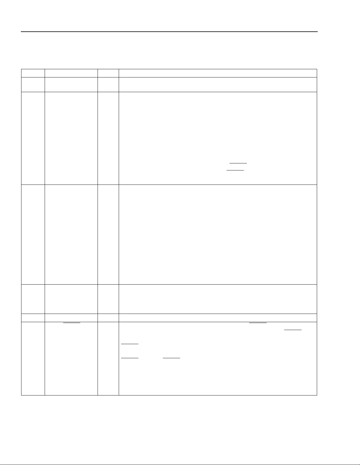
The European Telecommunications Standards Institute (ETSI) has identified a change in the requirement of
the power spectral density (PSD) for Basic Rate Interface ISDN.
Section A.12.4, Power Spectral Density, of ETSI TS080 states the following:
■ The upper boundary of the power spectral density of the transmitted signal shall be as shown in Figure 1,
below.
■ Measurements to verify compliance with this requirement are to use a noise power bandwidth of 1.0 kHz.
■ Systems deployed before January 1, 2000 do not have to meet this PSD requirement but shall meet the PSD
requirements as defined in ETR 080 edition 2. It is, however, expected that these systems will also meet the
PSD requirements of TS080 edition 3. Some narrowband violations could occur and should be tolerated.
PSD (dBm/Hz)
–20
–30
–40
–50
–60
–70
–80
–90
–100
–110
–120
–130
–140
0.001
0.010 1.0000.100 10.000
0.050
1.000
0.315
30.000
5.000
100.000
f (MHz)
5-7388F
Figure 1. Upper Boundary of Power Spectral Density from NT1 and LT
The existing SCNT1 family (T7234A, T7237A, and T7256A) of U-interface transceivers fully comply with this
standard.
Conformance to the above requirement has been fully verified, and test reports are available upon request.

For additional information, contact your Microelectronics Group Account Manager or the following:
INTERNET:
E-MAIL:
http://www.lucent.com/micro
docmaster@micro.lucent.com
N. AMERICA: Microelectronics Group, Lucent Technologies Inc., 555 Union Boulevard, Room 30L-15P-BA, Allentown, PA 18103
1-800-372-2447
, FAX 610-712-4106 (In CANADA:
1-800-553-2448
, FAX 610-712-4106)
ASIA PACIFIC: Microelectronics Group, Lucent Technologies Singapore Pte. Ltd., 77 Science Park Drive, #03-18 Cintech III, Singapore 118256
Tel. (65) 778 8833
, FAX (65) 777 7495
CHINA: Microelectr on ic s G r ou p, Lucent Tec hnologies (China) Co., Ltd., A-F2, 23/F, Zao Fong Univer s e B ui lding, 1800 Zhong Shan Xi Road, Shanghai
200233 P. R. China
Tel . ( 86) 21 6440 0468, ext. 316
, F A X ( 86) 21 6440 0652
JAPAN: Microelectronics Group, Lucent Technologies Japan Ltd., 7-18, Higashi-Gotanda 2-chome, Shinagawa-ku, Tokyo 141, Japan
EUROPE: Data Requests: MICROELECTRONICS GROUP DATALINE:
Tel. (81) 3 5421 1600
Technical Inquiries: GERMANY:
Lucent Technologies Inc. reserves the right to make changes to the product(s) or information contained herein without notice. No liability is assumed as a result of their use or application. No
rights under any patent accompany the sale of any such product(s) or information.
Copyright © 1998 Lucent Technologies Inc.
All Rights Reserved
Printed in U.S.A.
, FAX (81) 3 5421 1700
(49) 89 95086 0
FRANCE:
ITALY:
(33) 1 40 83 68 00
(39) 02 6608131
(Munich), UNITED KINGDOM:
Tel. (44) 1189 324 299
(Paris), SWEDEN:
(Milan), SPAIN:
(34) 1 807 1441
, FAX (44) 1189 328 148
(44) 1344 865 900
(46) 8 594 607 00
(Madrid)
(Stockholm), FINLAND:
(Ascot),
(358) 9 4354 2800
(Helsinki),
November 1998
AY99-004ISDN
(Must accompany DS97-410ISDN, DS97-411ISDN, DS97-412ISDN, and AY98-025ISDN)

Advisory
July 1998
T7234, T7237, and T7256
Data Sheet Advisory
(Refer to the T7234, T7237, and T7256 ISDN transceiver data sheets.)
The Technology and Telecommunications Standard sections below denote th e diff erenc es betw een the T723 4,
T7237, and T7256 and the T7234A, T7237A, and T7256A.
Technology
The T-7234- - -ML, T-7237- - -ML, and T-7256- - -ML2 are 0.9 µm CMOS technology devices.
■
The T-7234A- -ML, T-7237A- -ML, and T-7256A- -ML are 0.6 µm CMOS technology devices.
■
Telecommunication Standard
In 1996, the European Telecommunications Standards Institute (ETSI) added a microinterruption immunity
requirement to ETR 080 (Sections 5.4.5 and 6.2.5).
Section 5.4.5 in ETSI ETR 080 states the following:
A microinterruption is a temporary line interruption due to external mechanical activity on the copper wires
■
constituting the transmission path.
The effect of a microinterruption on the transmission system can be a failure of the digital transmission link.
■
The objective of this requirement is that the presence of a microinterruption of specified maximum length
■
shall not deactivate the sy stem , and the sy stem shal l acti vate if it has deactivated due to longer interruption.
Section 6.2.5 in ETSI ETR 080 states that:
A system shall tolerate a microinterruption up to t = 5 ms, when simulated with a repetition interval of
■
t = 5 ms.
The SCNT1 family of U-interface transceivers was upgraded to fully comply with this standard. The devices
have been given an A suffix (T7234A, T7237A, and T7256A).
A proposal was added to the Living List (which is intended to collect issues and observations for a possible
future update of ETSI ETR 080) to change the value of the microinterruption from 5 ms to 10 ms. The current
SCNT1 family of U-interface transceivers (T7234A/T7237A/T7256A) from Lucent Technologies Microelectronics Group meets and exceeds this new requirement.
The above change to the SCNT1 family of transceivers has been fully verified, and test reports are available
upon request.

T7234, T7237, and T7256
Data Sheet Advisory
Advisory
July 1998
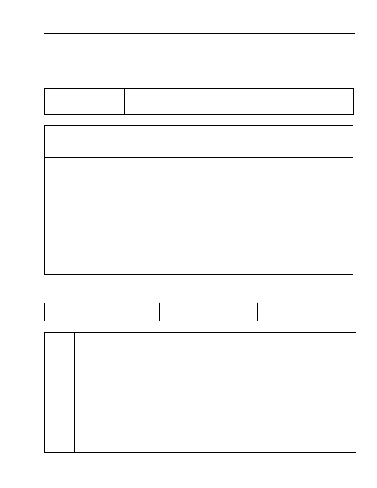
Application Circuit
Please change the v alu e of ca paci tor C 15 from 0.1 µF to 1 .0 µF in Fi gure 11 of the T7234 data sheet, Figure 17 of
the T7237 data sheet, and Figure 20 of the T7256 data sheet. The following schematic shows the correct value
(1.0 µF) for C15.
+5 V
SCNT1
OPTOIN
PIN
R8
17.8 kΩ
10 kΩ
6
5
R9
2.2 MΩ
R10
8
7
MLT CIRCUIT
U2
2
3
HCPL-0701
CA
1.0 µF
C15
1.0 µF
FOR NORTH AMERICAN
APPLICATIONS ONLY
(PLACE THIS CAPACITOR AS
CLOSE AS POSSIBLE TO THE LH1465)
R11
137 Ω
R12
137 Ω
ZD
8
TC
7
RS
6
PD
5
COM
LH1465AB
U3
PR+
PR–
T
R
1
2
3
4
RING TIP
R14
1.1 kΩ
2 W
R15
1.1 kΩ
2 W
5-7034(C)
Figure 1. MLT Circuit Showing New Placement of Zener Diode (ZD) and Capacitor (CA)
In the ILOSS mode (refer to ANSI T1.601 1992, Section 6.5.2), the NT generates a scrambled, framed, 2B1Q signal such as SN1 and SN2. When the ILOSS mode is applied to circuits with the LH1465, it was observed that for
some short loop lengths, the NT, once in the ILOSS mode, would not respond to further maintenance pulses until
the ILOSS timer expired. It was discovered that there is some portion of the transmitted 2B1Q signal from the NT
that passes through the LH1465 to the optoisolator. This causes the optoisolator to report incorrect dial pulses at
its output, and thus prevent the NT from properly exiting the ILOSS mode.
To correct this situation, the dropout voltage (voltage at the Tip/Ring needed to turn on the optoisolator) of the
optoisolator driver o n the LH 1465 is ra ised using the 3.6 V zener diode Z
Capacitor C
is a 1.0 µF ±10% tantalum chip capacitor, with a voltage rati ng of at least 16 V. CA is added to provide
A
(for e x ampl e ,
D
Motorola
* MMSZ4685T1).
a level of filtering for the transition points (turn-on or turn-off) of the optoisolator input voltage, which increases the
robustness of the circuit.
*
Motorola
is a registered t r a demark of Motorola Inc .
For additional information, contact your Microelectronics Group Account Manager or the following:
INTERNET:
E-MAIL:
N. AMERICA: Microelectronics Group, Lucent Technologies Inc., 555 Union Boulevard, Room 30L-15P-BA, Allentown, PA 18103
ASIA PACIFIC: Microelectronics Group, Lucent Technologies Singapore Pte. Ltd., 77 Science Park Drive, #03-18 Cintech III, Singapore 118256
CHINA: Microelectronics Group, Lucent Technologies (China) Co., Ltd., A-F2, 23/F, Zao Fong Universe Building, 1800 Zhong Shan Xi Road,
JAPAN: Microelectronics Group, Lucent Technologies Japan Ltd., 7-18, Higashi-Gotanda 2-chome, Shinagawa-ku, Tokyo 141, Japan
EUROPE: Data Requests: MICROELECTRONICS GROUP DATALINE:
Lucent Technologies Inc. reserves the right to make changes to the product(s) or information c ontained herein without notice. No liability is assumed as a result of their use or application. No
rights under any patent accompany the sale of any such product(s) or information.
Copyright © 1998 Lucent Technologies Inc.
All Rights Reserved
Printed in U.S.A.
July 1998
AY98-025ISDN (Replaces AY98-020ISDN)
http://www.lucent.com/micro
docmaster@micro.lucent.com
1-800-372-2447
Tel. (65) 778 8833
Shanghai 200233 P. R. China
Tel. (81) 3 5421 1600
Technical Inquiries: GERMANY:
, FAX 610-712-4106 (In CANADA:
, FAX (65) 777 7495
, FAX (81) 3 5421 1700
FRANCE:
(39) 2 6601 1800
IT ALY:
1-800-553-2448
Tel. (86) 21 6440 0468, ext. 316
(49) 89 95086 0
(33) 1 48 83 68 00
(Munich), UNITED KINGDOM:
(Paris), SWEDEN:
(Milan), SPAIN:
, FAX 610-712-4106)
, FAX (86) 21 6440 0652
Tel. (44) 1189 324 299
(46) 8 600 7070
(34) 1 807 1441
(Madrid)
, FAX (44) 1189 328 148
(44) 1344 865 900
(Stockholm), FINLAND:
(Bracknell),
(358) 9 4354 2800
(Helsinki),
(Must accompany DS97-410ISDN, DS97-411ISDN, and DS97-412ISDN)

Data Sheet
February 1998
T7237 ISDN U-Interface Transceiver
Features
■
U-interface for ISDN basic rate (2B+D) systems
— Serial microprocessor and time-division multi-
plexed (TDM) bus interfaces
— Automatic embedded operations channel (EOC)
processing for ANSI T1.601 systems
— Low power consumption (See Table 36, on page
65, Question and Answers section, for detailed
power consumption information)
— Idle-mode support (35 mW typical)
— Automatic ANSI maintenance functions (quiet
mode and insertion loss mode)
— Conforms to ANSI T1.601 standard and ETSI
ETR 080 technical report
— 2B1Q four-level line code
— Board-level testability support
■
Serial microprocessor and TDM bus interfaces
— Supports inexpensive serial microprocessor
— Supports direct codec connection and voice/
data ports
— Allows access to 2B+D data on TDM bus
■
Other
— Single +5 V ( ± 5%) supply
— –40 ° C to +85 ° C
— 44-pin PLCC
Description
The Lucent Technologies Microelectronics Group
T7237 ISDN U-Interface Transceiver is intended for
use in ISDN U-interface terminal adapter (TA) equipment providing 2-wire termination of the network with
B- and D-channel data available via a TDM interface.
The T7237 is a derivative of the T7256 device, and
thus, its operation is essentially identical to the
T7256, except for the absence of an S/T-interface.
The T7237 conforms to the ANSI T1.601 standard
and ETSI ETR 080 technical report for the U-interface. The single +5 V CMOS device is packaged in a
44-pin plastic leaded chip carrier (PLCC).

Data Sheet
T7237 ISDN U-Interface Transceiver February 1998
Table of Contents
Contents Page
Features ....................................................................................................................................................................1
Description ................................................................................................................................................................1
Pin Information ..........................................................................................................................................................5
Application Overview.................................................................................................................................................9
Functional Overview................................................................................................................................................10
U-Interface Frame Structure....................................................................................................................................10
Bit Assignments.......................................................................................................................................................11
U-Interface Description............................................................................................................................................12
Microprocessor Interface Description......................................................................................................................13
Registers..........................................................................................................................................................13
Timing..............................................................................................................................................................27
Time-Division Multiplexed (TDM) Bus Description..................................................................................................29
Clock and Data Format....................................................................................................................................29
Frame Strobe...................................................................................................................................................29
Data Flow Matrix Description...................................................................................................................................30
B1-, B2-, D-Channel Routing...........................................................................................................................30
Loopbacks...............................................................................................................................................................31
Modes of Operation.................................................................................................................................................32
STLED Description..................................................................................................................................................33
EOC State Machine Description..............................................................................................................................35
ANSI Maintenance Control Description...................................................................................................................35
Board-Level Testing .................................................................................................................................................35
External Stimulus/Response Testing.......................................................................................................................36
Application Briefs.....................................................................................................................................................37
T7237 Reference Circuit..................................................................................................................................37
Using the T7237 in a TA Environment .............................................................................................................41
T7237 Configuration........................................................................................................................................41
Interfacing the T7237 to the Motorola 68302...................................................................................................43
Absolute Maximum Ratings.....................................................................................................................................48
Handling Precautions ..............................................................................................................................................48
Recommended Operating Conditions .....................................................................................................................48
Electrical Characteristics.........................................................................................................................................49
Power Consumption.........................................................................................................................................49
Pin Electrical Characteristics...........................................................................................................................49
Crystal Characteristics.....................................................................................................................................50
Timing Characteristics.............................................................................................................................................51
Switching Test Input/Output Wavef orm............................................................................................................53
Outline Diagram.......................................................................................................................................................54
44-Pin PLCC....................................................................................................................................................54
Ordering Information................................................................................................................................................54
Questions and Answers...........................................................................................................................................55
Introduction......................................................................................................................................................55
U-Interface.......................................................................................................................................................55
Miscellaneous..................................................................................................................................................62
Glossary ..................................................................................................................................................................67
Standards Documentation.......................................................................................................................................71
2 Lucent Technologies Inc.

Data Sheet
February 1998 T7237 ISDN U-Interface Transceiver
Table of Contents
(continued)
Figures Page
Figure 1. Block Diagram............................................................................................................................................5
Figure 2. Pin Diagram................................................................................................................................................5
Figure 3. Applications of T7237.................................................................................................................................9
Figure 4. U-Interface Frame and Superframe .........................................................................................................11
Figure 5. U-Interface Superframe Bit Groups..........................................................................................................11
Figure 6. U-Interface Quat Example........................................................................................................................12
Figure 7. Functional Register Map (Addresses)......................................................................................................13
Figure 8. Functional Register Map (Bit Assignments).............................................................................................14
Figure 9. NEC and Motorola Microprocessor Port Connections..............................................................................27
Figure 10. Intel Microprocessor Port Connections ..................................................................................................27
Figure 11. Synchronous Microprocessor Port Interface Format..............................................................................28
Figure 12. TDM Bus Time-Slot Format....................................................................................................................30
Figure 13. B1-, B2-, D-Channel Routing..................................................................................................................30
Figure 14. Location of the Loopback Configurations (Reference ITU-T I.430 Appendix I)......................................31
Figure 15. STLED Control Flow Diagram................................................................................................................34
Figure 16. External Stimulus/Response Configuration............................................................................................36
Figure 17. T7237 Reference Circuit ........................................................................................................................38
Figure 18. T7237 TA Application Block Diagram.....................................................................................................41
Figure 19. MC68302 to T7237 Interface Diagram...................................................................................................43
Figure 20. T7237/MC68302 Interface Circuit...........................................................................................................45
Figure 21. T7237/MC68302 Interface Timing..........................................................................................................46
Figure 22. TDM Bus Timing.....................................................................................................................................51
Figure 23. Timing Diagram Referenced to F...........................................................................................................52
Figure 24. RESET
Figure 25. Switching Test Waveform.......................................................................................................................53
Figure 26. Transceiver Impedance Limits ...............................................................................................................57
Timing Diagram.........................................................................................................................52
Lucent Technologies Inc. 3

Data Sheet
T7237 ISDN U-Interface Transceiver February 1998
Table of Contents
(continued)
Tables Page
Table 1. Pin Descriptions ..........................................................................................................................................6
Table 2. U-Interface Bit Assignment ........................................................................................................................11
Table 3. Global Device Control—Device Configuration (Address 00h) ...................................................................15
Table 4. Global Device Control—U-Interface (Address 01h) ..................................................................................16
Table 5. Global Device Control (Address 02h) ........................................................................................................17
Table 6. Data Flow Control—U and S/T B Channels (Address 03h) .......................................................................18
Table 7. Data Flow Control—D Channels and TDM Bus (Address 04h) .................................................................18
Table 8. TDM Bus Timing Control (Address 05h) ....................................................................................................19
Table 9. Control Flow State Machine Control—Maintenance/Reserved Bits (Address 06h) ..................................20
Table 10. Control Flow State Machine Status (Address 07h) .................................................................................21
Table 11. Control Flow State Machine Status—Reserved Bits (Address 08h) .......................................................21
Table 12. EOC State Machine Control—Address (Address 09h) ...........................................................................22
Table 13. EOC State Machine Control—Information (Address 0Ah) ......................................................................23
Table 14. EOC State Machine Status—Address (Address 0Bh) ............................................................................23
Table 15. EOC State Machine Status—Information (Address 0Ch) .......................................................................23
Table 16. U-Interface Interrupt Register (Address 0Dh) ..........................................................................................24
Table 17. U-Interface Interrupt Mask Register (Address 0Eh) ................................................................................25
Table 18. Maintenance Interrupt Register (Address 0Fh) .......................................................................................25
Table 19. Maintenance Interrupt Mask Register (Address 10h) ..............................................................................26
Table 20. Global Interrupt Register (Address 11h) .................................................................................................26
Table 21. Microprocessor Mode ..............................................................................................................................32
Table 22. STLED States .........................................................................................................................................33
Table 23. T7237 Reference Schematic Parts List ...................................................................................................39
Table 24. Line-Side Resistor Requirements ...........................................................................................................40
Table 25. Motorola MC68302 SCC Options ............................................................................................................43
Table 26. Channel Selection Criteria ......................................................................................................................44
Table 27. Power Consumption ................................................................................................................................49
Table 28. Digital dc Characteristics (Over Operating Ranges) ...............................................................................49
Table 29. Fundamental Mode Crystal Characteristics ............................................................................................50
Table 30. Internal PLL Characteristics ....................................................................................................................50
Table 31. TDM Bus Timing ......................................................................................................................................51
Table 32. Clock Timing ............................................................................................................................................52
Table 33. RESET
Table 34. Power Dissipation Variation .....................................................................................................................64
Table 35. Power Dissipation of CKOUT...................................................................................................................64
Table 36. Power Consumption ................................................................................................................................65
Timing .........................................................................................................................................52
4 Lucent Technologies Inc.

Data Sheet
February 1998 T7237 ISDN U-Interface Transceiver
Description
(continued)
µP INTERFACE
µP INTERFACE &
REGISTERS
CONTROL FLOW STATE
MACHINE
DATA FLOW MATRIX
TDM BUS INTERFACE
TDM BUS INTERFACE
Figure 1. Block Diagram
eoc
STATE
MACHINE
U TRANSCEIVER
ANSI
MAINTENANCE
DECODER
CRYSTAL
OSC.
2-WIRE
2B1Q
U-INTERFACE
15.36011
MHz
5-2292.b (C)
Pin Information
TDMDI
TDMDO
TDMCLK
GND
INT
SDI
V
DDD
SDO
SCK
GND
CKOUT
VDDD
FS
ILOSS
6
54 4041424344123
7
8
9
10
D
11
12
13
14
15
16
D
17
19 2018 2827262524232221
X1
VDDO
GNDO
STLED
OPTOIN
T7237
X2
VDDA
GNDD
NC
HIGHZ
RESET
NC
GNDA
VDDA
NC
GNDA
NC
GNDA
39
38
37
36
35
34
33
32
31
30
29
VRCM
VDDA
SDINP
SDINN
HP
LON
GNDA
VDDA
LOP
HN
VRN
VRP
5-2296.b (C)
Figure 2. Pin Diagram
Lucent Technologies Inc. 5
—
—
Data Sheet
T7237 ISDN U-Interface Transceiver February 1998
Pin Information
(continued)
Table 1. Pin Descriptions
Pin Symbol Type* Name/Function
1, 10,
GND
D
Digital Ground. Ground leads for digital circuitry.
16
2 OPTOIN
u
Optoisolator Input. Pin accepts CMOS logic level maintenance pulse
I
streams. These pulse streams typically are generated by an optoisolator
that is monitoring the U loop. Pulse patterns on this pin are digitally filtered
for 20 ms before being considered valid and are then decoded and interpreted using the ANSI maintenance state machine requirements. If AUTOCTL
= 1 (register GR0, bit 3, default), the internal state machine decodes pulse
trains and implements the required maintenance states automatically. If
AUTOCTL = 0, the pulse trains are decoded internally, but the microprocessor must implement the maintenance state as indicated by the maintenance interrupts (register MIR0). If the OPTOIN pin is being used for
implementing maintenance functions, the ILOSS
pin should not be used
(i.e., it should be held high). Instead, the ILOSS register bit should be used
(register CFR0, bit 0). An internal 100 k Ω pull-up resistor is on this pin.
3 STLED O Status LED Driver. Output pin for driving an LED (source/sink 4.0 mA) that
indicates the device status. The four defined states are low, high, 1 Hz flashing, and 8 Hz flashing (flashing occurs at 50% duty cycle). See the STLED
Description section for a detailed explanation of these states.
Also, this pin indicates device sanity upon power-on/RESET, as follows:
■
If SCK = 0 (pin 15) after a device RESET (which sets AUTOACT = 0 in
register GR0 bit 6, turning on autoactivation), STLED will toggle at an
8 Hz rate for at least 0.5 s, signifying an activation attempt. If the activation attempt succeeds, it will continue to flash per the normal start-up
sequence (see STLED Description section).
4FSO
5, 13 V
6 ILOSS
u
* I
= input with internal pull-up.
DDD
u
I
■
If SCK = 1 (pin 15) after a device RESET, STLED will go low for 1 s (flash
of life), indicating that the device is oper ational, and no activ ation attempt
will be made.
Frame Strobe. If TDMEN = 0 (register GR2, bit 5), this pin is a programma-
ble strobe output used to indicate appearance of B- and/or D-channel data
on the TDM bus. Polarity, offset, and duration of FS are programmable
through the microprocessor interface (see register TDR0).
Digital Power. 5 V ± 5% power supply pins for digital circuitry.
Insertion Loss Test Control (Active-Low) . The ILOSS
pin is used to control SN1 tone transmission for maintenance. The OPTOIN and ILOSS pins
should not be used at the same time (i.e., OPTOIN should be held high when
ILOSS is active). This pin would typically be used if an external ANSI maintenance decoder is being used, in which case the decoder output drives the
ILOSS pin. The ILOSS pin is ignored, and the functionality is controlled by
the ILOSS bit (register CFR0, bit 0) if AUTOCTL = 0 (register GR0, bit 3).
Internal 100 k Ω pull-up resistor on this pin.
0—U transmitter sends SN1 tone continuously.
1—No effect on device operation.
6 Lucent Technologies Inc.

—
—
Data Sheet
February 1998 T7237 ISDN U-Interface Transceiver
Pin Information
(continued)
Table 1. Pin Descriptions (continued)
Pin Symbol Type* Name/Function
7 TDMDI
u
TDM Data In. If TDMEN = 0 (register GR2, bit 5), this pin is the TDM bus 2B+D data
I
input synchronous with TDMCLK. An internal 100 k Ω pull-up resistor is on this pin.
8 TDMDO O TDM Data Out. If TDMEN = 0, this pin is the 2.048 MHz TDM bus 2B+D data output
synchronous with TDMCLK.
9 TDMCLK O TDM Clock. If TDMEN = 0, this pin is the 2.048 MHz TDM clock output synchronous
with U-interface (if active) or is free-running.
11 INT
O Serial Interface Microprocessor Interrupt (Active-Low). Interrupt output for micro-
processor. Any active, unmasked bit in interrupt registers UIR0 or MIR0 will cause INT
to go low. The bits in the interrupt registers UIR0 and MIR0 will be set on a true condition, independent of the state of the corresponding mask bits. If a masked, active interrupt bit is subsequently unmasked, the INT
pin will go low to indicate an interrupt for that
condition. Reading UIR0 or MIR0 clears the entire register and forces INT high for
50 µ s. After this interval, INT will again reflect the state of any unmasked bit in these
registers. The global interrupt register (GIRO) provides a summary status of the UIR0
and MIR0 interrupt registers and indicates if one of the registers currently has an active,
unmasked interrupt bit.
12 SDI
d
Serial Interface Data Input. Data input for microprocessor interface.
I
14 SDO O Serial Interface Data Output. Data output for microprocessor interface. This pin is
3-stated at all times except for when a microprocessor read from the T7237 is taking
place.
d
15 SCK
Serial Interface Clock. Clock input for microprocessor interface.
I
17 CKOUT O Clock Output. Clock output function to drive other board components. Powerup default
state is high impedance to minimize power consumption. Programmable via microprocessor register (register GR0, bits 1 and 2) to provide 15.36 MHz output or 10.24 MHz
output. If U-interface is active, the 10.24 MHz output is synchronous with U-interface
timing.
DDO
O
Crystal Oscillator Ground. Ground lead for crystal oscillator.
Crystal Oscillator Power. Power supply lead for crystal oscillator.
18 GND
19 V
20 X1 O Crystal #1. Crystal connection #1 for 15.36 MHz oscillator.
21 X2 I Crystal #2. Crystal connection #2 for 15.36 MHz oscillator.
u
* I
= input with internal pull-up; I
d
= input with internal pull-down.
Lucent Technologies Inc. 7

Data Sheet
T7237 ISDN U-Interface Transceiver February 1998
Pin Information
(continued)
Table 1. Pin Description (continued)
Pin Symbol Type* Name/Function
22, 33,
VDDA — Analog Power. 5 V ± 5% power supply leads for analog circuitry.
39, 42
23 NC O No Connect. Do not use as a tie point.
24 NC O No Connect. Do not use as a tie point.
25, 34,
GNDA — Analog Ground. Ground leads for analog circuitry.
40, 41
26 NC I No Connect. Do not use as a tie point.
27 NC I No Connect. Do not use as a tie point.
28 VRCM — Common-Mode Voltage Reference for U-Interface Circuits. Connect a 0.1 µF ±
20% capacitor to GND
A (as close to the device pins as possible).
29 VRP — Positive Voltage Reference for U-Interface Circuits. Connect a 0.1 µF ± 20% ca-
pacitor to GNDA (as close to the device pins as possible).
30 VRN — Negative Voltage Reference for U-Interface Circuits. Connect a 0.1 µF ± 20% ca-
pacitor to GNDA (as close to the device pins as possible).
31 HN I Hybrid Negative Input for U-Interface. Connect directly to negative side of U-inter-
face transformer.
32 LOP O Line Driver Positive Output for U-Interface. Connect to the U-interface transformer
through a 16.9 Ω ± 1% resistor.
35 LON O Line Driver Negative Output for U-Interface. Connect to the U-interface transform-
er through a 16.9 Ω ± 1% resistor.
36 HP I Hybrid Positive Input for U-Interface. Connect directly to positive side of U-inter-
face transformer.
37 SDINN I Sigma-Delta A/D Negative Input for U-Interface. Connect via an 820 pF ± 5% ca-
pacitor to SDINP.
38 SDINP I Sigma-Delta A/D Positive Input for U-Interface. Connect via an 820 pF ± 5% ca-
pacitor to SDINN.
43 RESET
d
Reset (Active-Low). Asynchronous Schmitt trigger input. Reset halts data transmis-
I
sion, clears adaptive filter coefficients, resets the U-transceiver timing recovery circuitry, and sets all microprocessor register bits to their default state. During reset, the
U-interface transmitter produces 0 V and the output impedance is 135 Ω at tip and
ring. The RESET pin can be used to implement quiet mode maintenance testing (refer
to pin 2 for more description). The states of pins 11, 12, and 15 (INT, SDI, and SCK,
respectively) are latched on the rising edge of RESET. (See corresponding pin descriptions.) An internal 100 kΩ pull-down resistor is on this pin. RESET must be held
low for 1.5 ms after power-on. Device is fully functional after an additional 1 ms.
44 HIGHZ
u
High-Impedance Control (Active-Low). Control of the high-impedance function. An
I
internal 100 kΩ pull-up resistor is on this pin. Note: This pin does not 3-state the analog outputs.
0—All digital outputs enter high-impedance state.
1—No effect on device operation.
u
* I
= input with internal pull-up; Id = input with internal pull-down.
8 Lucent Technologies Inc.

Data Sheet
February 1998 T7237 ISDN U-Interface Transceiver
Application Overview
The T7237 is intended for use in ISDN networks as part of a terminal adapter (TA), providing 2-wire termination of
the network with available voice and/or data ports. The 2B+D data is accessible by the TDM highway, and the
device is configured using the serial microprocessor interface. Figure 3 shows the TA application.
PAL
TDM
OPTO-
T7237
SERIAL µP
INTERFACE
SCP
3
SCC
68302/360
MICROPROCESSOR
ISOLATOR
dc TERMINA TION, MLT
Figure 3. Applications of T7237
LH1465
SHARED
MEMORY
PC BUS
U-
INTERFA CE
5-4416 (F)
Lucent Technologies Inc. 9

Data Sheet
T7237 ISDN U-Interface Transceiver February 1998
Functional Overview
The T7237 device provides three major interfaces for
information transfer: the U-interface, the microprocessor interface, and the time-division multiplexed (TDM)
bus interface (see Figure 1).
The architecture of the T7237 allows for a flexible combination of automatically and manually controlled functions. A control flow state machine and an EOC state
machine can be independently enabled or disabled.
When enabled, these circuit blocks automatically perform their functions while ignoring the associated control bits in the microprocessor registers. When
disabled, the control bits are made available to the
microprocessor for manipulation. At all times, the status bits are available to the microprocessor and the
2B+D data can be routed via the data flow matrix.
The microprocessor interface is a serial communications port consisting of input data (SDI), output data
(SDO), input clock (SCK), and an output interrupt pin
). The microprocessor interface supports synchro-
(INT
nous communication between the T7237 and an inexpensive microprocessor with a serial port. The interrupt
is maskable via the onboard microprocessor interrupt
mask registers. The internal register set controls various functions including information routing between
interfaces, auto-EOC processing, maintenance testing, microprocessor interrupt masks, activation of the
TDM bus, and frame strobe timing.
The TDM interface consists of a TDM bus data clock
(TDMCLK), input data (TDMDI), output data (TDMDO),
and frame strobe (FS). The 2B+D data is transmitted
and received in fixed time slots on the TDM bus; however, the frame strobe output lead is programmable to
support a wide variety of devices (codecs, HDLC processors, asynchronous interfaces) f or direct connection
on the TDM bus. When the TDM bus is activated, pins
4, 7, 8, and 9 form the bus interface.
The EOC state machine, when enabled, automatically
performs the EOC channel functions as described in
the ANSI requirements. When disabled, control of the
EOC channel is passed to the microprocessor via the
appropriate microprocessor register bits.
The ANSI maintenance controller can operate in fully
automatic or in fully manual mode. In automatic mode,
the device decodes and responds to maintenance
states according to the ANSI requirements. In manual
mode, the device is controlled by an external maintenance decoder that drives the RESET and ILOSS pins
to implement the required maintenance states.
The control flow state machine performs the functions
of reserved bit insertion, automatic implementation of
the ANSI maintenance state machine, and automatic
prioritization of multiple requests, such as reset, activation, maintenance, etc. Some bits that are normally
controlled by the control flow state machine can be
forced to their active state by writing the appropriate
register (i.e., register GR1). When the control flow state
machine is disabled (via the AUTOCTL bit in register
GR0), the only change in the operation is that reserved
bit control and ANSI maintenance control are passed
directly to the microprocessor via register CFR0.
When the T7237 is powered on and there is no activity
on the U-interfaces (i.e., no pending activation
request), it automatically enters a low-power IDLE
mode in which it consumes an average of 35 mW.
This mode is exited automatically when an activation or
U maintenance request occurs from either the microprocessor or the U-interfaces. The T7237 provides a
board-level test capability that allows functional verification. Finally, an LED driver output indicates the status of the device during operation.
U-Interface Frame Structure
Data is transmitted over the U-interface in 240-bit
groups called U frames. Each U frame consists of an
18-bit synchronization word or inverted synchronization
word (SW or ISW), 12 blocks of 2B+D data (216 bits),
and six overhead bits (M bits). A U-interface superframe consists of eight U frames grouped together . The
beginning of a U superframe is indicated by the
inverted sync word (ISW). The six overhead bits (M1—
M6) from each of the eight U frames, when taken
together, form the 48 M bits. Figure 4 shows how U
frames, superframes, and M bits are arranged.
Of the 48 M bits, 24 bits form the embedded operations
channel (EOC) for sending messages from the LT to
the NT and responses from the NT to the LT. There are
two EOC messages per superframe with 12 bits per
EOC message (EOC1 and EOC2). Another 12 bits
serve as U-interface control and status bits (UCS). The
last 12 bits form the cyclic redundancy check (CRC)
which is calculated over the 2B+D data and the M4 bits
of the previous superframe. Figure 4 and Table 2 show
the different groups of bits in the superframe.
10 Lucent Technologies Inc.

Data Sheet
February 1998 T7237 ISDN U-Interface Transceiver
U-Interface Frame Structure (continued)
U-FRAME SPAN = 1.5 ms
ISW[18] (2B+D) x 12 [ 216 bits] M[6]
U-SUPERFRAME SPAN = 12 ms
U1 U2 U3 U4 U5 U6 U7 U8
U-INTERFACE M BITS [48]
5-2476 (C)
Figure 4. U-Interface Frame and Superframe
Bit # 1—18 19—234 235 236 237 238 239 240
Frame # Sync 12(2B+D) M1 M2 M3 M4 M5 M6
1 ISW
2
3
4
5
6
7
8
SW
EOC1
2B+D
EOC2
CONTROL & STATUS (UCS)
crc
Figure 5. U-Interface Superframe Bit Groups
Bit Assignments
Table 2. U-Interface Bit Assignment
Bit # 1—18 19—234 235 236 237 238 239 240
Frame # Sync 12(2B+D) M1 M2 M3 M4 M5 M6
1 ISW 2B+D EOCa1 EOCa2 EOCa3 act R1, 5 R1, 6
2 SW 2B+D EOCdm EOCi1 EOCi2 dea (ps1)* R2, 5 febe
3 SW 2B+D EOCi3 EOCi4 EOCi5 R3, 4 (ps2)* crc1 crc2
4 SW 2B+D EOCi6 EOCi7 EOCi8 R4, 4 (ntm)* crc3 crc4
5 SW 2B+D EOCa1 EOCa2 EOCa3
R5, 4 (cso)*
6 SW 2B+D EOCdm EOCi1 EOCi2 R6, 4 crc7 crc8
7 SW 2B+D EOCi3 EOCi4 EOCi5 uoa (sai)* crc9 crc10
8 SW 2B+D EOCi6 EOCi7 EOCi8
aib (nib)*
†
crc5 crc6
‡
crc11 crc12
* LT(NT). Values in parentheses () indicate meaning at the NT.
† cso is fixed at 0 by the device to indicate both cold- and warm-start capability.
‡ nib is fixed at 1 by the device to indicate the link is normal.
Lucent Technologies Inc. 11

Data Sheet
T7237 ISDN U-Interface Transceiver February 1998
U-Interface Description
At the U-interface, the T7237 conforms to ANSI T1.601
and ETSI ETR 080 when used with the proper line
interface circuitry. The T7237 Reference Circuit
description in the Application Briefs section of this document describes a detailed example of a U-interface
circuit design.
The 2B1Q line code provides a four-level (quaternary)
pulse amplitude modulation code with no redundancy.
Data is grouped into pairs of bits for conversion to quaternary (quat) symbols. Figure 6 shows an example of
this coding method.
The U-interface transceiver section provides the 2B1Q
line coder (D/A conversion), pulse shaper, line driver,
first-order line balance network, clock regeneration,
and sigma-delta A/D conversion. The line driver, when
connected to the proper transformer and interface circuitry , generates pulses which meet the required 2B1Q
templates. The A/D converter is implemented by using
a double-loop, sigma-delta modulator.
The U transceiver block also takes input from the data
flow matrix and formats this information for the U-interface (see Figure 1). During this formatting, synchronization bits for U framing are added and a scrambling
algorithm is applied. This data is then transferred to the
2B1Q encoder for transmission over the U-interface.
Signals received from the U-interface are first passed
through the sigma-delta A/D converter, and then sent
to the digital signal processor for more extensiv e signal
processing. The block provides decimation of the
sigma-delta output, linear and nonlinear echo cancellation, automatic gain control, signal detection, phase
shift interpolation, decision feedback equalization, timing recovery, descrambling, and line-code polarity
detection. The decision feedback equalizer circuit provides the functionality necessary for proper operation
on subscriber loops with bridged taps.
A crystal oscillator provides the 15.36 MHz master
clock for the device. The on-chip, phase-locked loop
provides the ability to synchronize the chip to the line
rate.
The U-interface provides rapid cold-start and warmstart operation. F rom a cold-start, the device is typically
operational within four seconds. The interface supports
activation/deactivation, and when properly deactivated,
it stores the adaptive filter coefficients permitting a
warm-start on the next activation request. A w arm-start
typically requires 200 ms for the device to become
operational.
–1
QUAT SYMBOL
BIT CODING
+3
+1
–3
–101+310+111–300–300+111+310–300–101–101+111–101–300+310+310–101+1
11
5-2294 (C)
Figure 6. U-Interface Quat Example
12 Lucent Technologies Inc.

Data Sheet
February 1998 T7237 ISDN U-Interface Transceiver
Microprocessor Interface Description
The microprocessor interface, used to control and
monitor the device, is compatible with most generalpurpose serial microprocessor interfaces using a synchronous mode of transmission. Transmission from the
microprocessor to the T7237 occurs in a 2-b yte f ormat,
the first byte representing read/write and register
address command information and the second byte
being write data or don’t cares for a read operation.
Transmission from the T7237 to the microprocessor
carries register data only. The interrupt line to the
microprocessor is maskable and can be used to signal
the microprocessor to initiate a register read or write
operation. A more detailed description of the operation
follows, and detailed timing information is given in the
Timing Characteristics section.
ADDRESS
00000
00001
00010
R/WGR0
R/WGR1
R/WGR2
GLOBAL DEVICE CONTROL — DEVICE CONFIGURATION
GLOBAL DEVICE CONTROL — U-INTERFACE
GLOBAL DEVICE CONTROL
Registers
The on-chip registers are divided by major circuit block
and by status and control function. Microprocessor register control bits associated with the control flow state
machine, EOC state machine, and multiframing controller are ignored when those blocks are enabled (the device controls the blocks automatically). When the blocks
are disabled, the control bits are used to drive device
operations. The functional summary of the registers and
bits is shown in Figure 7 and Figure 8.
00011
00100
00101
00110
00111
01000
01001
01010
01011
01100
10011
10100
10111
11000
R/WDFR0
R/WDFR1
TDR0 R/W TDM BUS TIMING CONTROL
R/WCFR0
RCFR1
RCFR2
R/WECR0
R/WECR1
RECR2
RECR3
UIR0 R
UIR1 R/W
MIR0 R
MIR1 R/W
DATA FLOW CONTROL — U B CHANNELS
DATA FLOW CONTROL — D CHANNELS & TDM BUS
CONTROL FLOW SM CONTROL — MAINTEN./RSV. BITS
CONTROL FLOW SM STATUS
CONTROL FLOW SM STATUS — RESERVED BITS
eoc STATE MACHINE CONTROL — ADDRESS
eoc STATE MACHINE CONTROL — INFORMATION
eoc STATE MACHINE STATUS — ADDRESS
eoc STATE MACHINE STATUS — INFORMATION
U-INTERFACE INTERRUPT REGISTER
U-INTERFACE INTERRUPT MASK REGISTER
MAINTENANCE INTERRUPT REGISTER
MAINTENANCE INTERRUPT MASK REGISTER
11001
GIR0 R GLOBAL INTERRUPT REGISTER
5-2299.a (C)
Figure 7. Functional Register Map (Addresses)
Lucent Technologies Inc. 13

Data Sheet
T7237 ISDN U-Interface Transceiver February 1998
Microprocessor Interface Description (continued)
Registers (continued)
R/W BIT 7 BIT 6 BIT 5 BIT 4 BIT 3 BIT 2 BIT 1 BIT 0REG
R/W
GR0
GR1
GR2
DFR0
DFR1
TDR0
CFR0
CFR1
CFR2
ECR0
ECR1
ECR2
ECR3
UIR0
UIR1
MIR0
MIR1
RESERVED AUTOACT — AUTOEOC AUTOCTL CRATE1 CRATE0 RESET
R/W
R/W
R/W
R/W
R/W
R/W
R
R
R/W
R/W
R
R
R
R/W
R
R/W
RGIR0
SAI1 SAI0 XPCY ACTT NTM PS1 PS2 LPBK
— ACTSEL TDMEN U2BDLN — — — —
— — — — UXB21 UXB20 UXB11 UXB10
TDMDU TDMB2U TDMB1U — — — — UXD
— — — — FSP FSC2 FSC1 FSC0
— — R64T R25T R16T R15T AFRST ILOSS
— AIB FEBE NEBE UOA OOF XACT ACTR
— R64R R54R R44R R34R R15R R16R R15R
CCRC U2BDLT UB2LP UB1LP DMT A1T A2T A3T
I1T I2T I3T I4T I5T I6T I7T I8T
— — — — DMR A1R A2R A3R
I1R I2R I3R I4R I5R I6R I7R I8R
—
— — TSFINTM RSFINTM OUSCM BERRM ACTSCM EOCSCM
— — — — — EMINT ILINT QMINT
— — — — — EMINTM ILINTM QMINTM
—— —— —
—
TSFINT RSFINT OUSC BERR
MINT — UINT
ACTSC
EOCSC
Figure 8. Functional Register Map (Bit Assignments)
5-2483.a (C)
14 Lucent Technologies Inc.

Data Sheet
February 1998 T7237 ISDN U-Interface Transceiver
Microprocessor Interface Description (continued)
Registers (continued)
Table 3. Global Device Control—Device Configuration (Address 00h)
Reg R/W Bit 7 Bit 6 Bit 5 Bit 4 Bit 3 Bit 2 Bit 1 Bit 0
GR0 R/W RES AUTOACT — AUTOEOC AUTOCTL CRATE1 CRATE0 RESET
Default State on
Register Bit Symbol Name/Description
GR0 0 RESET Reset. Same function as external RESET pin, except the state of the SCK, INT,
GR0 2—1 CRATE[1:0] CKOUT Rate Control.
GR0 3 AUTOCTL Auto Control Enable. Enables automatic control of ANSI maintenance and re-
GR0 4 AUTOEOC Automatic EOC Processor Enable. Enables EOC state machine which imple-
GR0 6 AUTOACT Automatic Activation Control. Upon a 1-to-0 transition of the AUTOACT bit, the
GR0 7 — Reserved. Set to 1.
RESET
1 SCK 1 1 1 1 1 1
and SDI pins are not checked. Assertion of this bit halts data transmission, clears
adaptive filter coefficients, and sets all microprocessor register bits (except itself)
to their default state. The microprocessor must write this bit back to a 1 to bring
the T7237 out of its RESET state. During reset, the U-interface transmitter produces 0 V and the output impedance is 135 Ω at tip and ring.
0—Reset.
1—No effect on device operation (default).
00—Not used.
01—10.24 MHz synchronous with U-interface (if active); otherwise, free-run-
ning.
10—15.36 MHz free-running.
11—3-state (default).
served bit insertion. When AUTOCTL = 1, register CFR0 is ignored and the control flow state machine automatically controls ANSI maintenance functions and
reserved bit insertion. When AUTOCTL = 0, the microprocessor controls ANSI
maintenance functions and reserved bit insertion via register CFR0.
0—CFR0 functions controlled manually by microprocessor.
1—CFR0 functions controlled automatically.
ments EOC processing per the ANSI standard. When AUTOEOC = 1, registers
ECR0—ECR1 are ignored. The EOC state machine only responds to addresses
000 and 111 as valid addresses.
0—EOC state machine disabled.
1—EOC state machine enabled (default).
control flow state machine attempts one activation of the U-interface. After the activation attempt, this bit is internally set to 1, automatically. If the SCK pin is low
on the rising edge of RESET
is made (see SCK pin description in Table 1). Multiple activation attempts can be
made by repeatedly writing 0s to this bit.
1—No activation attempt.
0—One activation attempt.
1—Default.
, AUTOACT is written to 0 and one activation attempt
Lucent Technologies Inc. 15

Data Sheet
T7237 ISDN U-Interface Transceiver February 1998
Microprocessor Interface Description (continued)
Registers (continued)
Table 4. Global Device Control—U-Interface (Address 01h)
Reg R/W Bit 7 Bit 6 Bit 5 Bit 4 Bit 3 Bit 2 Bit 1 Bit 0
GR1 R/W SAI1 SAI0 XPCY ACTT NTM PS1 PS2 LPBK
Default State on RESET
Register Bit Symbol Name/Description
GR1 0 LPBK U-Interface Analog Loopback. Controls loopback of U-interface data stream at
GR1 1 PS2 Power Status #2. Controls PS2 bit in transmit U-interface data stream if TDMEN
GR1 2 PS1 Power Status #1. Controls PS1 bit in transmit U-interface data stream if TDMEN
GR1 3 NTM NT Test Mode. Controls ntm bit in transmit U-interface data stream and
GR1 4 ACTT Transmit Activation. Controls act bit in transmit U-interface data
GR1 5 XPCY Transparency. Controls data being transmitted at U-interface.
GR1 7—6 SAI[1:0] S/T-Interface Activity Indicator Control. Controls sai bit in transmit U-interface
11101111
the line interface. Loopback turns off the echo canceler and reconfigures the receive scrambler to match the transmit scrambler. The line should be disconnected
before this loopback test. This ensures that a sufficiently large echo is generated
so that the device can detect the echo as received data and synchronize to it.
0—U-interface analog loopback.
1—No effect on device operation (default).
= 0 (register GR2, bit 5). If TDMEN = 1, PS2 bit is ignored. For ANSI T1.601 applications, PS1 and PS2 indicate the NT power status via the following messages:
PS1 PS2 Power Status
0 0 Dying gasp.
0 1 Primary power out.
1 0 Secondary power out.
1 1 All power normal (default).
= 0 (register GR2, bit 5). If TDMEN = 1, PS1 bit is ignored. See PS2 bit definition.
indicates if the NT is in a customer-initiated test mode.
0—NT is currently in a customer-initiated test mode.
1—No effect on device operation (default).
stream.
0—No effect on device operation (default).
1—Ready to transmit.
0—Enable data transparency.
1—No effect on device operation (default).
data stream. For ANSI T1.601 applications, the sai bit is set to 1 to indicate to the
network that there is activity (INFO 1 or INFO 3) at the S/T reference point. Since
some switch software expects to see sai = 1 before establishing layer 1 transparency, it is good practice to force sai = 1 in U-terminal adapter applications to emulate the presence of a TE. The SAI[1:0] bits provide the following options for
controlling the sai bit:
00—Forces sai to 0 on the U-interface.
01—Forces sai to 1 on the U-interface.
11—Forces sai to 0 on the U-interface.
16 Lucent Technologies Inc.

Data Sheet
February 1998 T7237 ISDN U-Interface Transceiver
Microprocessor Interface Description (continued)
Registers (continued)
Table 5. Global Device Control (Address 02h)
Reg R/W Bit 7 Bit 6 Bit 5 Bit 4 Bit 3 Bit 2 Bit 1 Bit 0
GR2 R/W — ACTSEL TDMEN U2BDLN — — — —
Default State on RESET
1
Register Bit Symbol Name/Description
GR2 4 U2BDLN Nontransparent 2B+D Loopback Control. When 0, this bit causes a nontrans-
parent loopback of 2B+D data from U receiver to U transmitter upstream of the
data flow matrix. Note that this loopback path is not as close to the S/T-interface
as the transparent loopback initiated by U2BDLT (register ECR0, bit 6). This loopback may be useful for test purposes. When this bit is set, the upstream data (NT
to LT direction) will be forced to all 1s until either ACTR = 1 (register CFR1, bit 0)
or XPCY = 0 (register GR1, bit 5).
GR2 5 TDMEN TDM Bus Select. Selects functions of pins 4, 7, 8, and 9.
GR2 6 ACTSEL ACT Mode Select. Controls the state of the transmitted ACT bit when an EOC
loopback 2 (2B+D loopback) is requested. The loopback 2 occurs automatically
if AUTOEOC = 1 (register GR0, bit 4). Otherwise, bit U2BDLT (register ECR0, bit
6) must be set to 0. The initial state of ACTSEL is determined by the state of the
ACTMODE/INT
ACTMODE/
INT pin
111111
0—2B+D loopback. All 1s 2B+D data is automatically generated towards the
TE.
1—No loopback (default).
0—TDM bus functions. Pins 4, 7, 8, and 9 configured as FS, TDMDI, TDMDO,
and TDMCLK, respectively. See DFR1 and TDR0 registers for TDM bus
programming details. Microprocessor register bits GR11, GR12, and GR20
control the PS2, PS1, and FT functions.
1—No TDM bus. Pins 4, 7, 8, and 9 configured as SYN8K/LBIND, FTE, PS2E,
and PS1E, respectively (default).
pin on the rising edge of RESET.
0—act = 0 during loopback 2 (per ANSI T1.601). The data received at the NT
is looped back towards the LT as soon as the 2B+D loopback is enabled.
1—act = 1 during loopback 2 (per ETSI ETR 080). The data received by the NT
is not looped back towards the LT until after ACT = 1 is received from the
LT. Prior to this time, 2B+D data toward the LT is all 1s.
Lucent Technologies Inc. 17

Data Sheet
T7237 ISDN U-Interface Transceiver February 1998
Microprocessor Interface Description (continued)
Registers (continued)
Table 6. Data Flow Control—U and S/T B Channels (Address 03h)
Reg R/W Bit 7 Bit 6 Bit 5 Bit 4 Bit 3 Bit 2 Bit 1 Bit 0
DFR0 R/W ————UXB21 UXB20 UXB11 UXB10
Default State on RESET
Register Bit Symbol Name/Description
DFR0 1—0 UXB1[1:0] U-Interface Transmit Path Source for B1 Channel. Refer to point #1
DFR0 3—2 UXB2[1:0] U-Interface Transmit Path Source for B2 Channel. Refer to point #1
11111111
in Figure 13.
00—Not used.
01—TDM bus.
10—All 1s.
11—Not used.
in Figure 13.
00—Not used.
01—TDM bus.
10—All 1s.
11—Not used.
Table 7. Data Flow Control—D Channels and TDM Bus (Address 04h)
Bits 2—7 are enabled only if TDMEN = 0 (register GR2, bit 5). The TDMCLK and FS outputs are activated if any
one of bits 2—7 is enabled. The TDMDO output is activated during time slots enabled by programming bits 2—7.
Reg R/W Bit 7 Bit 6 Bit 5 Bit 4 Bit 3 Bit 2 Bit 1 Bit 0
DFR1 R/W TDMDU TDMB2U TDMB1U ————UXD
Default State on RESET
Register Bit Symbol Name/Description
DFR1 0 UXD U-Interface Transmit Path Source for D Channel. Refer to point #1 in Figure 13.
DFR1 5 TDMB1U TDM Bus Transmit Control for B1 Channel from U-Interface. Refer to point #2 in
DFR1 6 TDMB2U TDM Bus Transmit Control for B2 Channel from U-Interface. Refer to point #2 in
DFR1 7 TDMDU TDM Bus Transmit Control for D Channel from U-Interface. Refer to point #2 in
11111111
0—TDM bus.
1—Reserved.
Figure 13. Controls transmit time slot allocated on TDM bus for B1 channel derived
from U-interface receiver.
0—Time slot enabled.
1—Time slot disabled (high impedance) (default).
Figure 13. Controls transmit time slot allocated on TDM bus for B2 channel derived
from U-interface receiver.
0—Time slot enabled.
1—Time slot disabled (high impedance) (default).
Figure 13. Controls transmit time slot allocated on TDM bus for D channel derived from
U-interface receiver.
0—Time slot enabled.
1—Time slot disabled (high impedance) (default).
18 Lucent Technologies Inc.

Data Sheet
February 1998 T7237 ISDN U-Interface Transceiver
Microprocessor Interface Description (continued)
Registers (continued)
Table 8. TDM Bus Timing Control (Address 05h)
Bits 0—4 are enabled only if TDMEN = 0 (register GR2, bit 5) and one or more of bits DFR1[2:7] are set to 0.
Reg R/W Bit 7 Bit 6 Bit 5 Bit 4 Bit 3 Bit 2 Bit 1 Bit 0
TDR0 R/W ————FSPFSC2 FSC1 FSC0
Default State on RESET
Register Bit Symbol Name/Description
TDR0 2—0 FSC[2:0] Frame Strobe (FS) Control. Selects location of strobe envelope within
TDR0 3 FSP Frame Strobe (FS) Polarity.
———— 1111
TDM bus time slots.
000—Reserved.
001—U-interface 2B+D channel strobe (18-bit envelope).
010—Reserved.
011—U-interface B2 channel strobe (8-bit envelope).
100—Reserved.
101—U-interface D channel strobe (2-bit envelope).
110—Reserved.
111—U-interface B1 channel strobe (8-bit envelope) (default).
0—Active-low envelope.
1—Active-high envelope (default).
Lucent Technologies Inc. 19

Data Sheet
T7237 ISDN U-Interface Transceiver February 1998
Microprocessor Interface Description (continued)
Registers (continued)
Table 9. Control Flow State Machine Control—Maintenance/Reserved Bits (Address 06h)
This register has no effect on device operation if AUTOCTL = 1 (register GR0, bit 3).
Reg R/W Bit 7 Bit 6 Bit 5 Bit 4 Bit 3 Bit 2 Bit 1 Bit 0
CFR0 R/W — — R64T R25T R16T R15T AFRST ILOSS
Default State on RESET
Register Bit Symbol Name/Description
CFR0 0 ILOSS Insertion Loss Test Control. The insertion loss test mode is initiated by setting
CFR0 1 AFRST Adaptive Filter Reset. U transceiver reset. Assertion of this bit halts U-interface
CFR0 3—2 R[16:15]T Transmit Reserved Bits. Controls R
CFR0 4 R25T Transmit Reserved Bit. Controls R2, 5 in transmit U-interface data stream.
CFR0 5 R64T Transmit Reserved Bit. Controls R6, 4 in transmit U-interface data stream.
——111111
AFRST = 0 and ILOSS = 0, and then setting AFRST = 1. When enabled, the
U-interface transmitter continuously transmits the sequence SN1. The U-interface
receiver remains reset. The U-interface transceiver performs an internal reset
when the ILOSS bit returns to its inactive state.
0—U-transmitter sends SN1 tone continuously.
1—No effect on device operation (default).
data transmission and clears adaptive filter coefficients. During AFRST, the U
transmitter produces 0 V and has an output impedance of 135 Ω. If the microprocessor interface is being used, the AFRST bit should be used to place the device
in quiet mode for U-interface maintenance procedures. Assertion of AFRST does
not reset the microprocessor register bits or the U-interface timing recovery.
0—U transceiver reset.
1—No effect on device operation (default).
1, 6 and R1, 5 in transmit U-interface data
stream.
11—(Default.)
1—(Default.)
1—(Default.)
20 Lucent Technologies Inc.

Data Sheet
February 1998 T7237 ISDN U-Interface Transceiver
Microprocessor Interface Description (continued)
Registers (continued)
Table 10. Control Flow State Machine Status (Address 07h)
Reg R/W Bit 7 Bit 6 Bit 5 Bit 4 Bit 3 Bit 2 Bit 1 Bit 0
CFR1 R — AIB FEBE NEBE UOA OOF XACT ACTR
Register Bit Symbol Name/Description
CFR1 0 ACTR Receive Activation. Follows act bit in receive U-interface data stream.
0—Pending activation.
1—Ready to transmit.
CFR1 1 XACT U Transceiver Active.
0—Transceiver not active.
1—Transceiver starting up or active.
CFR1 2 OOF Out of Frame.
0—U-interface out of frame.
1—Normal.
CFR1 3 UOA U-Interface Only Activation. Follows uoa bit in receive U-interface data stream.
0—U-interface only for activation.
1—U-interface and S/T-interface for activation.
CFR1 4 NEBE Near-End Block Error. Follows nebe bit in receive U-interface data stream.
0—CRC error detected in previously received U frame.
1—No error.
CFR1 5 FEBE Far-End Block Error. Follows febe bit in receive U-interface data stream.
0—Error detected at LT.
1—No error.
CFR1 6 AIB Alarm Indication Bit. Follows aib in receive U-interface data stream.
0—Failure of intermediate 2B+D transparent element.
1—Transmission path established between LT and NT.
Table 11. Control Flow State Machine Status—Reserved Bits (Address 08h)
Reg R/W Bit 7 Bit 6 Bit 5 Bit 4 Bit 3 Bit 2 Bit 1 Bit 0
CFR2 R — R64R R54R R44R R34R R25R R16R R15R
Register Bit Symbol Name/Description
CFR2 1—0 R[16:15]R Receive Reserved Bits. Follows R1, 5 and R1, 6 in receive U-interface
data stream.
CFR2 2 R25R Receive Reserved Bits. Follows R2, 5 in receive U-interface data
stream.
CFR2 6—3 R[64:54:44:34]R Receive Reserved Bits. Follows R3, 4; R4, 4; R5, 4; and R6, 4 in receive
U-interface data stream.
Lucent Technologies Inc. 21

Data Sheet
T7237 ISDN U-Interface Transceiver February 1998
Microprocessor Interface Description (continued)
Registers (continued)
Table 12. EOC State Machine Control—Address (Address 09h)
This register has no effect on device operation if AUTOEOC = 1 (register GR0, bit 4).
Reg R/W Bit 7 Bit 6 Bit 5 Bit 4 Bit 3 Bit 2 Bit 1 Bit 0
ECR0 R/W CCRC U2BDLT UB2LP UB1LP DMT A1T A2T A3T
Default State on RESET
Register Bit Symbol Name/Description
ECR0 0—2 A[3:1]T Transmit EOC Address.
ECR0 3 DMT Transmit EOC Data or Message Indicator.
ECR0 4 UB1LP U-Interface Loopback of B1 Channel Control. Control for U-interface
ECR0 5 UB2LP U-Interface Loopback of B2 Channel Control. Control for U-interface
ECR0 6 U2BDLT Transparent 2B+D Loopback Control. When activated, this bit causes
ECR0 7 CCRC Corrupt Cyclic Redundancy Check. Used to corrupt the CRC informa-
11111000
000—NT address (default).
111—Broadcast address.
0—Data.
1—Message (default).
transparent B1 loopback. UB1LP and UB2LP may be enabled concurrently.
0—B1 channel loopback from U-interface receive to U-interface trans-
mit upstream of data flow matrix.
1—No loopback (default).
transparent B2 loopback. UB1LP and UB2LP may be enabled concurrently.
0—B2 channel loopback from U-interface receive to U-interface trans-
mit upstream of data flow matrix.
1—No loopback (default).
a transparent 2B+D loopback.
0—Transparent 2B+D loopback: The microprocessor must clear the
data flow matrix (UXB10 = UXB11 = UXB20 = UXB21 = UXD = 1) for
proper operation of the loopback.
1—No loopback (default).
tion transmitted at the U-interface.
0—Corrupt CRC generation.
1—Generate correct CRC (default).
22 Lucent Technologies Inc.

Data Sheet
February 1998 T7237 ISDN U-Interface Transceiver
Microprocessor Interface Description (continued)
Registers (continued)
Table 13. EOC State Machine Control—Information (Address 0Ah)
This register has no effect on device operation if AUTOEOC = 1 (register GR0, bit 4).
Reg R/W Bit 7 Bit 6 Bit 5 Bit 4 Bit 3 Bit 2 Bit 1 Bit 0
ECR1 R/W I1T I2T I3T I4T I5T I6T I7T I8T
Default State on RESET
Register Bit Symbol Name/Description
ECR1 0—7 I[8:1]T Transmit EOC Information. These bits are transmitted as the EOC
Table 14. EOC State Machine Status—Address (Address 0Bh)
This register contains the currently received EOC address and data/message indicator bits independent of the state
of AUTOEOC (register GR0, bit 4).
11111111
channel message when in manual EOC mode.
See EOC State Machine Description section for a list of possible EOC
messages.
Reg R/W Bit 7 Bit 6 Bit 5 Bit 4 Bit 3 Bit 2 Bit 1 Bit 0
ECR2 R ————DMRA1RA2RA3R
Register Bit Symbol Name/Description
ECR2 0—2 A[3:1]R Receive EOC Address. These bits store the received EOC address.
000 = NT address.
001—110 = Intermediate element addresses.
111 = Broadcast address.
ECR2 3 DMR Receive EOC Data or Message Indicator.
0—Data.
1—Message.
Table 15. EOC State Machine Status—Information (Address 0Ch)
This register contains the currently received EOC information bits independent of the state of AUTOEOC (register
GR0, bit 4).
Reg R/W Bit 7 Bit 6 Bit 5 Bit 4 Bit 3 Bit 2 Bit 1 Bit 0
ECR3 R I1R I2R I3R I4R I5R I6R I7R I8R
Register Bit Symbol Name/Description
ECR3 0—7 I[8:1]R Receive EOC Information. Receive EOC channel message or data.
Lucent Technologies Inc. 23

Data Sheet
T7237 ISDN U-Interface Transceiver February 1998
Microprocessor Interface Description (continued)
Registers (continued)
Table 16. U-Interface Interrupt Register (Address 0Dh)
These bits are cleared during RESET
Reg R/W Bit 7 Bit 6 Bit 5 Bit 4 Bit 3 Bit 2 Bit 1 Bit 0
UIR0 R — — TSFINT RSFINT OUSC BERR ACTSC EOCSC
Register Bit Symbol Name/Description
UIR0 0 EOCSC EOC State Change on U-Interface. Activates (set to 1) when the re-
UIR0 1 ACTSC Activation/Deactivation State Change on U-Interface. Activates (set
UIR0 2 BERR Block Error on U-Interface. Activates (set to 1) when received signal
UIR0 3 OUSC Other U-Interface State Change. Activates (set to 1) when any of the
UIR0 4 RSFINT Receive Superframe Interrupt. Activates (set to 1) when the receive
UIR0 5 TSFINT Transmit Superframe Interrupt. Activates (set to 1) when the transmit
.
ceived EOC message changes state. Bit is cleared on read. See EOC
State Machine Description section for details.
0—No change in EOC state.
1—EOC state change.
to 1) during changes in the status bits monitoring U-interface activation
and deactivation (ACTR and XACT, register CFR1, bits 0 and 1). Bit
cleared on read.
0—No activation/deactivation activity.
1—Change in state of activation/deactivation bits.
contains either a near-end (NEBE = 0) or a far-end (FEBE = 0) block error. Bit cleared on read.
0—No block errors.
1—Block error.
following bits change state: OOF, UOA, AIB, and Rx, y (all reserved
U-interface status bits). Bit cleared on read.
0—No state change.
1—State change.
superframe boundary occurs. Bit cleared on read.
0 to 1—First 2B+D data of the receive U superframe.
superframe boundary occurs. Bit cleared on read.
0 to 1—First 2B+D data of the transmit U superframe.
24 Lucent Technologies Inc.
Data Sheet
February 1998 T7237 ISDN U-Interface Transceiver
Microprocessor Interface Description (continued)
Registers (continued)
Table 17. U-Interface Interrupt Mask Register (Address 0Eh)
Reg R/W Bit 7 Bit 6 Bit 5 Bit 4 Bit 3 Bit 2 Bit 1 Bit 0
UIR1 R/W — — TSFINTM RSFINTM OUSCM BERRM ACTSCM EOCSCM
Default State on RESET
Register Bit Symbol Name/Description
UIR1 0 EOCSCM EOC State Change on U-Interface Mask.
UIR1 1 ACTSCM Activation/Deactivation State Change on U-Interface Mask.
UIR1 2 BERRM Block Error on U-Interface Mask.
UIR1 3 OUSCM Other U-Interface State Change Mask.
UIR1 4 RSFINTM Receive Superframe Interrupt Mask.
UIR1 5 TSFINTM Transmit Superframe Interrupt Mask.
—— 1 1 1 1 1 1
0—EOCSC interrupt enabled.
1—EOCSC interrupt disabled (default).
0—ACTSC interrupt enabled.
1—ATCSC interrupt disabled (default).
0—BERR interrupt enabled.
1—BERR interrupt disabled (default).
0—OUSC interrupt enabled.
1—OUSC interrupt disabled (default).
0—RSFINT interrupt enabled.
1—RSFINT interrupt disabled (default).
0—TSFINT interrupt enabled.
1—TSFINT interrupt disabled (default).
Table 18. Maintenance Interrupt Register (Address 0Fh)
These bits are cleared during
Reg R/W Bit 7 Bit 6 Bit 5 Bit 4 Bit 3 Bit 2 Bit 1 Bit 0
MIR0 R —————EMINT ILINT QMINT
Register Bit Symbol Name/Description
MIR0 0 QMINT Quiet Mode Interrupt. Activates (set to 1) when the ANSI maintenance state machine
MIR0 1 ILINT Insertion Loss Interrupt. Activates (set to 1) when the ANSI maintenance state ma-
MIR0 2 EMINT Exit Maintenance Mode Interrupt. Activates (set to 1) when the ANSI maintenance
RESET.
detects a request on the OPTOIN pin for the device to enter the quiet mode. Bit is
cleared on read.
0—No quiet mode request.
1—Quiet mode requested.
chine has detected a request on the OPTOIN pin for the device to transmit the SN1 tone
on the U-interface. Bit is cleared on read.
0—No SN1 tone request.
1—SN1 tone requested.
state machine detects a request on the OPTOIN pin for the device to exit the current
maintenance mode. Bit is cleared on read.
0—No exit request.
1—Exit requested.
Lucent Technologies Inc. 25
Data Sheet
T7237 ISDN U-Interface Transceiver February 1998
Microprocessor Interface Description (continued)
Registers (continued)
Table 19. Maintenance Interrupt Mask Register (Address 10h)
Reg R/W Bit 7 Bit 6 Bit 5 Bit 4 Bit 3 Bit 2 Bit 1 Bit 0
MIR1 R/W — — — — — EMINTM ILINTM QMINTM
Default State on RESET
Register Bit Symbol Name/Description
MIR1 0 QMINTM Quiet Mode Interrupt Mask.
MIR1 1 ILINTM Insertion Loss Interrupt Mask.
MIR1 2 EMINTM Exit Maintenance Mode Interrupt Mask.
————— 1 1 1
0—QMINT interrupt enabled.
1—QMINT interrupt disabled (default).
0—ILINT interrupt enabled.
1—ILINT interrupt disabled (default).
0—EMINT interrupt enabled.
1—EMINT interrupt disabled (default).
Table 20. Global Interrupt Register (Address 11h)
These bits are cleared during
Reg R/W Bit 7 Bit 6 Bit 5 Bit 4 Bit 3 Bit 2 Bit 1 Bit 0
GIR0 R —————MINT — UINT
Register Bit Symbol Name/Description
GIR0 0 UINT U Transceiver Interrupt. Activates (set to 1) when any of the unmasked
GIR0 2 MINT Maintenance Interrupt. Activates (set to 1) when any of the unmasked
RESET.
U transceiver interrupt bits (register UIR0) activate.
0—No U transceiver interrupts.
1—U transceiver interrupt active.
maintenance interrupt bits (register MIR0) activate.
0—No maintenance interrupts.
1—Maintenance interrupt active.
26 Lucent Technologies Inc.
Data Sheet
February 1998 T7237 ISDN U-Interface Transceiver
Microprocessor Interface Description (continued)
Timing
The microprocessor interface is compatible with any microprocessor that supports a synchronous serial microprocessor port such as the following:
■ NEC
■ Motorola
■ Intel
1
75402
2
MC68HC05 and MC68302 SCP port
3
80C51
11
INT
15
SCK
T7237
14
SDO
12
SDI
INTERRUPT IN
CLOCK OUT
DATA IN
DATA OUT
MICROPROCESSOR
NEC OR
Motorola
5-2300 (C)
Figure 9. NEC and Motorola Microprocessor Port Connections
The synchronous interface consists of the microprocessor input clock (SCK), serial data input (SDI), and serial
data output (SDO). A microprocessor interrupt lead (INT) is also included. These connections are shown in Figure
9 for applications using either NEC or Motorola microprocessors. Figure 10 shows the connections for applications
using a multiplexed data out/in scheme such as the Intel 80C51 or equivalent.
INT
11
INTERRUPT IN
15
SCK
T7237
14
SDO
12
SDI
CLOCK OUT
INTEL 80C51
OR EQUIVALENT
DATA OUT/IN
5-2301 (C)
Figure 10. Intel Microprocessor Port Connections
1. NEC is a registered trademark of NEC Electronics, Inc.
2. Motorola is a registered trademark of Motorola, Inc.
3. Intel is a registered trademark of Intel Corporation.
Lucent Technologies Inc. 27

Data Sheet
T7237 ISDN U-Interface Transceiver February 1998
Microprocessor Interface Description (continued)
Timing (continued)
≤300 µs
≥10 µs
SCLK
Note: If SCLK is initially low, it must be held high for >300 µs before its first falling edge. From that point forward, the above timing applies.
12
SHIFT IN SAMPLE SHIFT IN
SDI
CA7 CA6 CA5 CA4 CA3 CA2 CA1 CA0
COMMAND
SDO
MSB LSB MSB LSB
34567
ADDRESS DATA SHIFT OUT
DON'T CARE
8
12345678
DI7 DI6 DI5 DI4 DI3 DI2 DI0DI1
DO7 DO6 DO5 DO4 DO3 DO2 DO0DO1
≥10 µs
1
CA7
5-2302 (C)
Figure 11. Synchronous Microprocessor Port Interface Format
Figure 11 shows the basic transfer format. All data
transfers are initiated by the microprocessor, although
the interrupt may indicate to the microprocessor that a
register read or write is required. The microprocessor
should normally hold the SCK pin high during inactive
periods and only make transitions during register transfers. The maximum clock rate of SCK is 960 kHz. Data
changes on the falling edge of SCK and is latched on
the rising edge of SCK.
Each complete serial transfer consists of 2 bytes
(8 bits/byte). The first byte of data received over the
SDI pin from the microprocessor consists of command/
address information that includes a 5-bit register
address in the least significant bit positions (CA4—
CA0) and a 3-bit command field in the most significant
bit positions (CA7—CA5). The byte is defined as follows:
■ Bits CA7—CA5: 001 = read, 010 = write, all other bit
patterns will be ignored.
■ Bits CA4—CA0: 00000 = register address 0, 00001
The data transmitted over the SDO pin to the microprocessor during the first byte transfer is a don't care for
both read and write operations. The second byte transmitted over the SDO pin consists of read data for CA7—
CA5 = 001 (read) or don't care information for CA7—
CA5 = 010 (write).
In order for the T7237 to recognize the identity (command/address or data) of the byte being received, it is
required that the time allowed to transfer an entire
instruction (time from the receipt of the first bit of the
command/address byte to the last bit of the data byte)
be limited to less than 300 µs. This limits the minimum
SCK rate to 60 kHz. If the complete instruction is
received in less than 300 µs, the T7237 accepts the
instruction immediately and is ready to receive the next
instruction after a 10 µs delay. If the complete instruction is not received within 300 µs, the bits received in
the previous 300 µs are discarded and the interface is
prepared to receive a new instruction after a 10 µs
delay. In addition, a minimum 10 µs delay must exist
between the command/address and data bytes.
= register address 1, etc.
The second byte of data received over the SDI pin consists of write data for CA7—CA5 = 010 (write) or don't
care information for CA7—CA5 = 001 (read).
28 Lucent Technologies Inc.

Data Sheet
February 1998 T7237 ISDN U-Interface Transceiver
Microprocessor Interface Description
(continued)
Timing (continued)
For microprocessors using a multiple xed data out/in pin
to drive SDI and SDO (as shown in Figure 8), a read
instruction to T7237 will require that the microprocessor data in/out pin be an output during the command/
address byte written to T7237, and then switch to an
input to read the data byte T7237 presents on the SDO
pin in response to the read command. In this case, the
microprocessor data in/out pin must 3-state within
1.46 µs of the final SCK rising edge of the command/
address byte to ensure that there is no contention
between the microprocessor data out pin and the
T7237 SDO pin.
Time-Division Multiplexed (TDM) Bus
Description
The TDM bus facilitates B1-, B2-, and D-channel communication between the T7237 and peripheral devices
such as codecs, HDLC processors, time-slot interchangers, synchronous data interfaces, etc. The following list is a subset of the devices that can connect
directly to the T7237 TDM bus:
strobe timing can be configured via the microprocessor
register bits FSC and FSP in register TDR0. Data
appearing and expected on the bus is controlled via the
B1-, B2-, and D-channel data flow register bits (registers DFR0 and DFR1). The TDMCLK and FS outputs
only become active if one or more of the TDM time
slots is enabled (see register DFR1, Table 7).
Clock and Data Format
The clock and data signals for the TDM bus are TDMCLK, TDMDO , and TDMDI (see Figure 12). TDMCLK is
a 2.048 MHz output clock. TDMDO is the 2B+D data
output for data derived from the U-interface receiver.
The TDMDO output driver is only active during a time
slot when it is driving data off-chip; otherwise, the output driver is 3-stated (this includes the 6-bit interval in
the D-channel octet). TDMDI is the 2B+D data input for
data used to drive the U-interface transmitter.
On both the TDMDO and TDMDI leads, three 8-bit time
slots are reserved for the B1-, B2-, and D-channels
associated with the U-interfaces. The relative locations
of the time slots are fixed; however, the frame strobe is
programmable. The total n umber of time slots a vailable
within each frame strobe period is 32. During unused
time slots, data on TDMDI is ignored and TDMDO is
3-stated.
■ Lucent T7570 and T7513 Codecs
■ Lucent T7270 Time-Slot Interchanger
■ Lucent T7121 HDLC Formatter
■ National Semiconductor*3070 Codec
The bus can be used to extract data from U-interface
receivers, process the data e xternally, and source data
to the appropriate transmitters with the processed data.
The bus can also be used to simply monitor 2B+D
channel data flow within the T7237 without modifying it.
The bus also supports board-level testing procedures
using in-circuit techniques (see the Board-Level Testing
section for more details). Upon powerup, the TDM bus
is not selected. Pins 4, 7, 8, and 9 form the TDM bus
when TDMEN is set to 0 (register GR2, bit 5).
The TDM bus consists of a 2.048 MHz output clock
(TDMCLK), data in (TDMDI), data out (TDMDO), and a
programmable frame strobe lead (FS). The frame
* National Semiconductor is a registered trademark of National
Semiconductor Corporation.
Frame Strobe
The FS frame strobe is a programmable output associated with the TDM bus. FS can be configured to serve
as an envelope strobe for any of the three reserved
time slots available on the bus: U-interface B1, B2, and
D . FS can also be prog rammed as a 2B+D env elope f or
the U-interface time slots. FS can be used to directly
drive a codec for voice applications or can be used to
control other external devices such as HDLC controllers.
Figure 12 shows the relationship between the TDMCLK, TDMDO, and TDMDI time slots, and the FS
strobe for some example programmable settings.
Detailed descriptions of TDM bus interface timing are
given in the Timing Characteristics section of this document.
Lucent Technologies Inc. 29

Data Sheet
T7237 ISDN U-Interface Transceiver February 1998
Time-Division Multiplexed (TDM) Bus Description (continued)
Frame Strobe (continued)
B27
B28
8-bit TIME SLOT
U-INTFC
D
D1
D2
RESERVED RESERVED RESERVED
5-2303a (C)
2B+D EXAMPLE
FSC = 001 AND
FSP = 1
B2 EXAMPLE
FSC = 011 AND
FSP = 1
TDMCLK
TDMDO/
TDMDI
FS
FS
U-INTFC
B11
B12
B13
B1
B14
B15
B16
B17
B18
U-INTFC
B2
B21
B22
B23
B24
B25
B26
Figure 12. TDM Bus Time-Slot Format
Data Flow Matrix Description
B1-, B2-, D-Channel Routing
The T7237 supports extremely flexible B1-, B2-, and D-channel routing among major circuit blocks in order to accommodate various applications. Channel routing is controlled via the data flow control registers, DFR0 and DFR1.
Figure 13 shows a block diagram of the device and the channel paths to and from the U transceiver and TDM bus
interface. Channel flow is determined by specifying the source of channel data at the two points shown in the figure:
(1) U transceiver transmit input and (2) TDM bus transmit input. Channel flow at the TDM bus receive input is determined, by default, from the settings at the other two points. A switch matrix within the data flow matrix block routes
channels to and from the specified points.
µP INTERFACE
µP INTERFACE
1
TRANSMIT
DATA FLOW
CONTROLLER
SWITCH MATRIX
RECEIVE
2
TDM BUS INTFC.
U TRANSCEIVER
TDM BUS INTERFACE
5-2304.b (C)
Figure 13. B1-, B2-, D-Channel Routing
30 Lucent Technologies Inc.

Data Sheet
February 1998 T7237 ISDN U-Interface Transceiver
Data Flow Matrix Description (continued)
B1-, B2-, D-Channel Routing (continued)
As an example, below are the register settings required
to configure the device as a U-interface terminal
adapter, with the B1, B2, and D channels in the U-interface made available on the TDM bus for monitoring:
■ TDMEN = 0 (enables TDM bus).
■ UXB1 = 01, UXB2 = 01, UXD = 0 (routes TDM bus
data to U-interface transmitter).
■ TDMB1U = TDMB2U = 0 (brings out B1 and B2
channels from U-interface to TDM bus).
■ TDMDU = 0 (D channel from U-interface brought out
on TDM bus).
TE1
4A
S
NT2 NT1
B1 3 B2
Loopbacks
The figure below shows the Lay er-1 loopbac ks that are
defined in ITU-T I.430, Appendix I and ANSI Specification T1.605, Appendix G. A complete discussion of
these loopbacks is presented in ITU-T I.430, Appendix
I.
If a U-interface transparent B1 or B2 loopback is
requested via an EOC message, the proper channel is
looped upstream of the data flow matrix. All other
device functions are unaffected.
If a U-interface transparent 2B+D loopback is
requested via an EOC message (loop 2 in Figure 14),
the 2B+D data will be looped as close to the T-interface
as possible.
TU
U
LT2C
TATE2
R
A
TE1 = ISDN terminal R = R reference point 2 2B+D channels
TE2 = Non-ISDN terminal S = S reference point 3 2B+D channels
TA = Terminal adapter T = T reference point 4 B1, B2
NT2 = Network termination 2 U = U reference point C B1, B2
NT1 = Network termination 1 B1 or B2 2B+D, B1, B2
LT = Line termination A 2B+D, B1, B2
S
4
Loopback Channel(s) Looped
Figure 14. Location of the Loopback Configurations (Reference ITU-T I.430 Appendix I)
5-2482 (C)
Lucent Technologies Inc. 31

Data Sheet
T7237 ISDN U-Interface Transceiver February 1998
Modes of Operation
The T7237 transceiver operates under microprocessor control through the serial interface. The T7237 automatically
handles U-interface activation, control, and maintenance according to the ANSI T1.601 standard.
In addition, the T7237 allows manual EOC and U overhead bit manipulation. The microprocessor port is accessed
via the SDI, SDO, and SCK pins (see Microprocessor Interf ace Description and Timing Characteristics sections for
details). Table 21 shows the transceiver control pins that are most relevant to the microprocessor.
Table 21. Microprocessor Mode
Pin Symbol Comment
2 OPTOIN Controlled by microprocessor bit AUTOCTL (register GR0).
4 FS Controlled by microprocessor bit TDMEN (register GR2).
6 ILOSS Controlled by microprocessor bit AUTOCTL (register GR0).
7 TDMDI Controlled by microprocessor bit TDMEN (register GR2).
8 TDMDO Controlled by microprocessor bit TDMEN (register GR2).
9 TDMCLK Controlled by microprocessor bit TDMEN (register GR2).
11 INT
12 SDI Serial data input for the microprocessor interface.
14 SDO Serial data output for the microprocessor interface.
15 SCK Master clock input for the microprocessor interface.
Interrupt output for the microprocessor interface.
32 Lucent Technologies Inc.

Data Sheet
February 1998 T7237 ISDN U-Interface Transceiver
STLED Description
The STLED pin is used to drive an LED and provides a
visual indication of the current state of the T7237. The
STLED control is typically configured to illuminate the
LED when STLED is LOW. This convention will be
assumed throughout this section.
Table 22 describes the three states of STLED, the list
of system conditions that produce the state, and the
corresponding ANSI states, as defined in ANSI T1.6011992 (Tables C1 and C4) and ETSI ETR 080-1992
(Tables A3 and I2).
Note: The ETSI state names begin with the letters NT
instead of H. Also, the ETSI state tables do not
include a state NT11 because it is considered
identical to state NT6. Table A3 of the ETSI
standard contains the additional states NT6A,
NT7A, and NT8A to describe states related to
the EOC loopback 2 (2B+D loopback). The
most likely ANSI state for each STLED state is
shown in bold typeface in Table 22.
Table 22. STLED States
The flow chart in Figure 15 illustrates the priority of the
logic signals which control the STLED pin. In the decision diamonds, those names in all capital letters
denote T7237 register bit names. The RESET,
AUTOCTL, and AUTOEOC are R/W bits controlled by
the user via the microprocessor interface. The XACT,
OOF, and aib bits are read-only bits determined by the
internal logic based on system events and can be monitored by the user via the microprocessor interface.
Other names in the decision diamonds (quiet mode,
ILOSS mode, Loop2) represent system conditions that
cannot be directly monitored or controlled by the microprocessor interface.
STLED State List of System Conditions that Can Cause STLED State Corresponding ANSI States
High (LED off) RESET (pin 43) = 0
AUTOCTL = 0 (register GR0, bit 3), or
AUTOEOC = 0 (register GR0, bit 4), or
STOA = 0 (register GR2, bit 7)
U not active H0, H1, H10, H12
8 Hz Flashing RESET = 0 (register GR0, bit 0)
Quiet mode active, or
ILOSS mode active
U activation attempt in progress H2, H3, H4
AIB = 0 (register CFR1, bit 6) H7, H8
EOC-initiated 2B+D loopback active NT6A*, NT7A*, NT8A*
1 Hz Flashing U active, S/T not fully active H6, H6(a), H7, H11, H8(a)†,
* These are ETSI DTR/TM-3002 states not yet defined in ANSI T1.601, although they are defined in re vised ANSI tab les which are currently on
the living list (i.e., not yet an official part of the standards document).
† State H8(a) is most likely when U-interface bit uoa = 0.
NA
NA
H8(b), H8(c)
Lucent Technologies Inc. 33

Data Sheet
T7237 ISDN U-Interface Transceiver February 1998
STLED Description (continued)
START
STLED = OFF
STLED = OFF
RESET
PIN LOW?
NO
YES
YES
AUTOCTL = 0
AUTOEOC = 0, OR
STOA = 0
NO
RESET = 0, QUIET
MODE = ACTIVE, OR ILOSS
MODE = ACTIVE
NO
U-INTERFACE
INACTIVE?
NO
U-INTERFACE
NOT SYCHRONIZED?
NO
YES
YES
YES
STLED = OFF
STLED = 8 Hz
STLED = 8 Hz
STLED = 8 Hz
Figure 15. STLED Control Flow Diagram
YES
aib = 0
NO
LOOP2 = ACTIVE?
NO
STLED = 1 Hz
YES
STLED = 8 Hz
5-3599.c (F)
34 Lucent Technologies Inc.

Data Sheet
February 1998 T7237 ISDN U-Interface Transceiver
EOC State Machine Description
The following list shows the eight EOC states defined
in ANSI T1.601 and ETSI ETR 080. The bit pattern
below represents the state of U-interface ov erhead bits
EOCi1—EOCi8, respectively (see Table 2).
01010000—Operate 2B+D loopback.
01010001—Operate B1 channel loopback.
01010010—Operate B2 channel loopback.
01010011—Request corrupt CRC.
01010100—Notify of corrupted CRC.
11111111—Return to normal (default).
00000000—Hold state.
10101010—Unable to comply.
Normally, the T7237 automatically handles the EOC
channel processing per the ANSI and ETSI standards.
There may be some applications where manual control
of the EOC channel is desired (e.g., equipment that is
meant to test the EOC processing of upstream elements by writing incorrect or delayed EOC data). This
can be accomplished by setting AUTOEOC = 0 (register GR0, bit 4). The EOC state change interrupt is
enabled by setting EOCSCM = 0 (register UIR1, bit 0).
This allows state changes in the received EOC messages (registers ECR2 and ECR3) to be indicated to
the microprocessor by the assertion of UINT = 1 (register GIR0, bit 0) and EOCSC = 1 (register UIR0, bit 0).
The microprocessor reads registers ECR2 and ECR3
to determine which received EOC bits changed. Then,
it updates the transmit EOC values by writing registers
ECR0 and ECR1 and takes appropriate action (e.g.,
enable a requested loopback). The total manual EOC
procedure consists of the following steps:
1. Microprocessor detects INT
2. Microprocessor reads GIR0 and determines that
the UINT bit is set.
pin going low.
The maximum time allowed from the assertion of the
INT
pin (step 1) until the completion of the last write
cycle to the EOC registers (step 8) is 1.5 ms.
ANSI Maintenance Control Description
The ANSI maintenance controller of the T7237 can
operate in fully automatic or in fully manual mode.
Automatic mode can be used in applications where
autonomous control of the metallic loop termination
(MLT) maintenance is desired. The MLT capability
implemented with the Lucent LH1465AB and an optocoupler provides a dc signature, sealing current sink,
and maintenance pulse-level translation for the testing
facilities. Maintenance pulses from the U-interface MLT
circuit are received by the OPTOIN pin and digitally filtered for 20 ms. The device decodes these pulses
according to ANSI maintenance state machine requirements and responds to each request automatically.
For example, the T7237 will place itself in the quiet
mode if six pulses are received from the MLT circuitry.
Microprocessor interrupts in register MIR0 are available for tracking maintenance events if desired.
Manual mode can be used in applications where an
external maintenance decoder is used to drive the
RESET
RESET pin places the device in quiet mode and the
ILOSS pin controls SN1 tone transmission. Maintenance events are not a vailab le in register MIR0 when in
manual mode.
Board-Level T esting
The T7237 provides several board-level testability features. For example, the HIGHZ pin 3-states all digital
outputs for bed-of-nails testing. Also , various loopbac ks
can be used to verify device functionality.
and ILOSS pins of the T7237. In this mode, the
3. Microprocessor reads UIR0 and determines that the
EOCSC bit is set.
4. Microprocessor reads ECR2.
5. Microprocessor reads ECR3.
6. Microprocessor interrupts newly received EOC
message and determines the appropriate response.
7. Microprocessor writes ECR0 based on results of
step 6.
8. Microprocessor writes ECR1 based on results of
step 6.
Lucent Technologies Inc. 35

Data Sheet
T7237 ISDN U-Interface Transceiver February 1998
External Stimulus/Response Testing
External data transparency of the B1, B2, and D channels can be verified by the combined use of the TDM
bus and microprocessor port. Data flow within the
device can be configured by the external controller
through the microprocessor port, and B1-, B2-, and Dchannel data can be transmitted into and received from
the device via the TDM bus. Using this method, arbitrary data patterns can be used to stimulate the device
and combinations of loopbacks can be exercised to
help detect and isolate faults. Figure 16 illustrates this
general-purpose testing configuration.
EXTERNAL TEST MACHINE
DATA FLOW
REGISTER
PROGRAMMING
TDMDI data can be routed through the device and
back to TDMDO at the U-interface. For looping at Uinterface, the procedure is as follows:
■ Disconnect the U-interface from the telephone net-
work.
■ Set TDMEN = 0 in register GR2, bit 5.
■ Set register DFR0 to 11110101.
■ Set register DFR1 to 00011110.
■ Set register TDR0 as required for the desired frame
strobe location and polarity.
Now, write LPBK in register GR1 to a 0. This causes
the chip to enter the U-interface loopback mode. Any
data entering the TDM highway on TDMDI will be
looped back (with some delay) on TDMDO.
µP INTERFACE
DATA FLOW
CONTROLLER
IMPLEMENTS DATA
PATH
TDM BUS INTERFACE
TDMDOTDMDI
DATA STIMULUS &
RECEIVED DATA
COMPARE
EXTERNAL TEST MACHINE
TRANSMIT
RECEIVE
U TRANSCEIVER
U-INTERFACE
OPEN
CIRCUITED
Figure 16. External Stimulus/Response Configuration
5-2305.a (C)
36 Lucent Technologies Inc.

Data Sheet
February 1998 T7237 ISDN U-Interface Transceiver
Application Briefs
T7237 Reference Circuit
A reference circuit illustrating the T7237 in a standard
application, including complete ANSI maintenance
support, is shown in Figure 17. A bill of materials for
the schematic is shown in Table 23. Note that specific
applications may vary depending on individual requirements.
U-Interface
The U-Interface attaches to the board at RJ-45 connector J1 (see Figure 17). F1 and VR2 provide overcurrent
and overvoltage protection, respectively. These two
devices in combination with transformer T1 provide
protection levels required by FCC Part 68 and UL*
1459. For an in-depth discussion of protection issues,
the following application notes are helpful.
1. “Overvoltage Protection of Solid-State Subscriber
Loop Circuits,” Lucent Analog Line Card Components Data Book (CA94-007ALC) 800-372-2447.
2. Protection of Telecommunications Customer
Premises Equipment, Raychem
415-361-6900.
C16 is a 1.0 µF dc blocking capacitor that is required
per ANSI T1.601, Section 7.5.2.3. The 250 V rating of
C16 is governed by the maximum breakdown voltage
of VR2, since the capacitor must not break do wn before
VR2. The resistance of R13 (21 Ω) and F1 (12 Ω) provides a total line-side resistance of 33 Ω, which is
required when using the Lucent 2754H2 transformer
(see the note at the end of Table 23 for information on
R13 values when using other transformers).
On the device side of the U-interface transformer, VR1
provides secondary overvoltage protection of 6.8 V.
Optional capacitors C13 and C14 provide commonmode noise suppression for applications that are
required to operate in the presence of high commonmode noise. R6 and R7 provide the necessary external
hybrid resistors.
†
Corporation,
MLT Circuit
The metallic loop termination (MLT) circuit (U3 and
related components in Figure 17) provides a dc termination for the loop per ANSI T1.601, Section 7.5. R14
and R15 are power resistors used to sink current during overvoltage fault conditions. The optoisolater (U2)
provides signal isolation and voltage translation of the
signaling pulses used for NT maintenance modes, per
T1.601, Section 6.5. The T7237 interprets these pulses
via an internal ANSI maintenance state machine, and
responds accordingly. For applications outside North
America, the MLT circuit is not required.
Status LED
D1 in Figure 17 is an LED that is controlled by the
STLED pin of the T7237 and indicates the status of the
device (activating, out-of-sync, etc.). Table 22 and Figure 15 of this data sheet details the possible states of
the STLED pin and the meaning of each state.
Power Status Leads
ANSI T1.601 Section 8.2.4 defines U-interf ace NT po wer status bits PS1 and PS2. These bits are transmitted
across the U-Interface via the U maintenance channel.
On the T7237, these bits are controlled b y pins 8 and 9
(PS2E and PS1E). When the TDM highw a y is used (TA
modes), the PS1/PS2 bits are controlled by internal registers that are written by an external microprocessor. In
general, power status monitoring circuitry is dependent
on various system parameters and requirements, and
must be designed based on the specific application’s requirements. For this reason, there is no power status
monitoring circuitry shown in this design. Instead, pullups R1 and R2 in Figure 17 are provided to force a default indication of primary and secondary power good
status.
* UL is a registered trademark of Underwriters Laboratories, Inc.
† Raychem is a registered trademark of Raychem Corporation.
Lucent Technologies Inc. 37
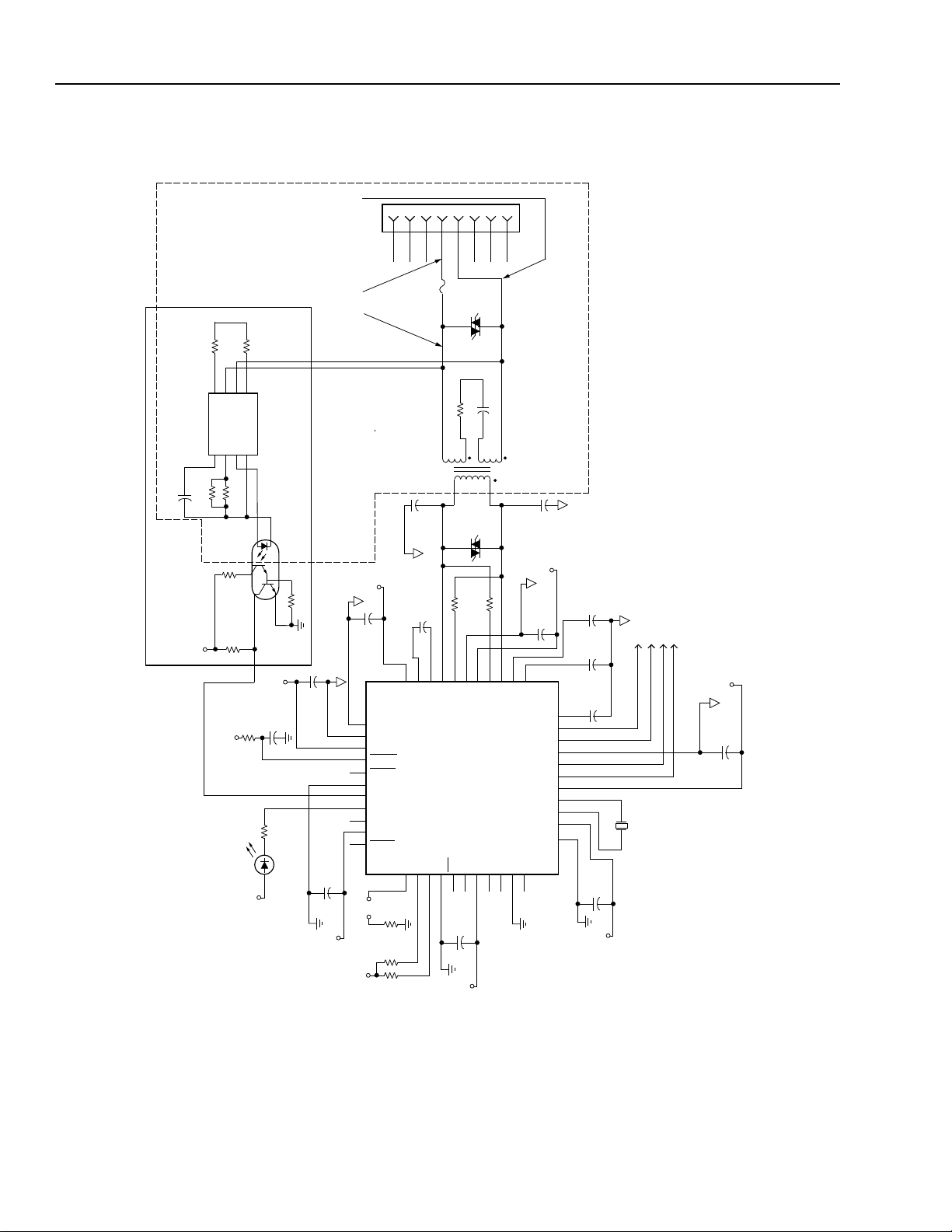
Data Sheet
T7237 ISDN U-Interface Transceiver February 1998
Application Briefs (continued)
T7237 Reference Circuit (continued)
R14
1.1 kΩ
2 W
LH1465AB
(PLACE THIS CAPACITOR AS
CLOSE AS POSSIBLE TO THE LH1465)
R11
137 Ω
C15
0.1 µF
MLT CIRCUIT
+5 V
123
4
T
R
PR+
PR–
U3
TCRSPD
COM
876
5
R12
137 Ω
U2
8
R10
10 kΩ
R8
17.8 kΩ
R5
+5 V
POR CIRCUIT
STATUS LED
R15
1.1 kΩ
2 W
FOR NORTH AMERICAN
2
3
HCPL-0701
7
5
6
R9
+5 VA
C5
1.0 µF
5.1 kΩ
R4
825 Ω
D1
+5 V
J1
TRACKS SHOULD BE 50 mils
NOTE: THE WIDTH OF THESE
APPLICATIONS ONLY
0.01 µF
+5 V
40
41
42
43
44
2
3
4
C10
GNDA
GNDA
RESET
HIGHZ
1
OPTOIN
STLED
VDDD
5
ILOSS
6
2
JMP1
1
+5 VA
0.01 µF
DDA
V
GNDD
FS
R3
R2
2.2 MΩ
C7
0.01 µF
C2
213
3938373635343332313029
789
5.1 kΩ
5.1 kΩ
4
F1
TR600-150
7
T1
C13
3300 pF
C9
820 pF
DDA
V
SDINP
SDINN
TDMDI
TDMDO
TDMCLK
10111213141516
5
VR2
SMP100-140
R13
21 Ω
1
VR1
SA6.0CA
R6
16.9 ΩR716.9 Ω
A
HP
LON
GND
U1
T7237
GNDD
INT
SDI
C1
0.01 µF
786
C16 1.0 µF
9106
5
LOP
VDDA
VDDD
SDO
HN
SCK
RJ-45
U-INTERFACE CIRCUIT
1:1.5
2754H2
C14
3300 pF
+5 VA
C11
0.01 µF
VRP
VRN
VRCM
28
NC
27
NC
26
GNDA
25
NC
24
NC
23
DDA
V
22
X2
21
X1
20
VDDO
19
GNDO
18
GNDDCKOUT
17
GROUND/POWER PLANES SHOULD NOT COME WITHIN
2.5 mm OF THE CIRCUITRY WITHIN THIS DASHED AREA
C12
0.1 µF
C8
0.1 µF
TPR
TNR
RPR
C6
C3
0.1 µF
RNR
X1
15.360 MHz
0.01 µF
+5 V
+5 VA
C4
0.01 µF
+5 V
R1
PRESENT
CIRCUIT IF
MONITORING
AND PS2E TO
CONNECT PS1E
POWER STATUS
5.1 kΩ
+5 V
5-4048.i (C)
Figure 17. T7237 Reference Circuit
38 Lucent Technologies Inc.

Data Sheet
February 1998 T7237 ISDN U-Interface Transceiver
Application Briefs (continued)
T7237 Reference Circuit (continued)
Table 23. T7237 Reference Schematic Parts List
Reference
Description Source Part #
Designator
C[1—4, 7,
Ceramic Chip Capacitor, 0.01 µF, 10%, 50 V, X7R
Kemet
1
C1206C103K5RAC
10, 11]
C5 Tantalum Chip Capacitor, 1.0 µF, 10%, 16 V Kemet T491A105K016AS
C[6, 8, 12,
Ceramic Chip Capacitor, 0.1 µF, 10%, 50 V, X7R Kemet C1206C104K5RAC
17]
C9 Ceramic Chip Capacitor, 820 pF, 5%, 50 V, NPO Kemet C0805C821J5GAC
C[13, 14] Ceramic Chip Capacitor, 3300 pF, 10%, 50 V, X7R Kemet C1206C332F5RAC
C15 Polyester Capacitor, 0.1 µF, 63 V, 10%
Philips
2
2222 370 12104
Note: Insulation resistance of this part must
be >2 GΩ.
C16 Capacitor, 1.0 µF, 250 V, 10%
Alternate: Philips 2222 373 41105
Vitramon
TMI (rep)
(215) 830-8500
D1 Green Surface-mount LED Hewlett
Packard
F1
5
Overcurrent Protector (Polyswitch
)
Alternate: Bel Fuse6 MJS 1.00A, (201) 432-0463
Raychem
(415) 361-6900
3
4
, via
VJ9253Y105KXPM
HSMG-C650
TR600-150
See Note at the end of this table.
J1 RJ-45 8-pin Modular Jack (standard height)
Molex
7
15-43-8588
JMP1 Two-position Header with Shorting Jumper Multiple —
R[1—3, 5] SMC Resistor, 5.1 kΩ, 1/8 W, 5%
Dale
8
CRCW1206512J
R4 SMC Resistor, 825 kΩ, 1/8 W, 1% Dale CRCW12068250F
R[6, 7] SMC Resistor, 16.9 kΩ, 1/8 W, 1% Dale CRCW120616R9F
R8 SMC Resistor, 17.8 kΩ, 1/8 W, 1% Dale CRCW12061783F
R9 SMC Resistor, 2.2 MΩ, 1/8 W, 5% Dale CRCW1206225J
R[10, 18, 19] SMC Resistor, 10 kΩ, 1/8 W, 5% Dale CRCW1206103J
[R11, 12] SMC Resistor, 137 Ω, 1/8 W, 1% Dale CRCW12061370F
R13 SMC Resistor, 21.0 Ω, 1 W, 1% Dale WSC-1
1. Kemet is a registered trademark of Kemet Laboratories Company, Inc.
2. Philips is a registered trademark of Philips Manufacturing Company.
3. Vitramon is a registered trademark of Vitramon, Inc.
4. Hewlett Packard is a registered trademark of Hewlett-Packard Company.
5. Polyswitch is a registered trademark of Raychem Corporation.
6. Bel and Bel Fuse are registered trademarks of Bel Fuse, Inc.
7. Molex is a registered trademark of Molex, Inc.
8. Dale is a registered trademark of Dale Electronics, Inc.
Lucent Technologies Inc. 39

Data Sheet
T7237 ISDN U-Interface Transceiver February 1998
Application Briefs (continued)
T7237 Reference Circuit (continued)
Table 23. T7237 Reference Schematic Parts List (continued)
Reference
Description Source Part #
Designator
R14, 15 SMC Resistor,
Dale WSC-2
1.1 kΩ, 2 W, 5%
T1 ISDN U-interface Trans-
former
Lucent 2754H2
Alternates (See footnote at the end of this table.):
Lucent 2754K2 (1500 Vrms breakdown)
Lucent 2809A (for EN60950 compliance)
10
Valor
PT4084 (619) 537-2500
Midcom 671-7759 (605) 886-4385
U1 T7237 IC, 44-pin PLCC Lucent —
U2 Optocoupler Hewlett Packard HCPL-0701
U3 ISDN dc Termination IC Lucent LH1465AB
VR1 Transient Voltage
Suppressor
SGS-Thomson
11
SM6T6V8CA
Alternates:
Motorola SA6.5CA, P6KE6.8CA, P6KE7.5CA
VR2 Transient Voltage
Suppressor
X1 15.36 Crystal Saronix
SGS-Thomson SMP100-140
Alternate:
12
Teccor
P1602AB (972) 580-7777
SRX5144
(415) 856-6900
Alternates:
MTRON
13
4044-001 (605) 665-9321
2B Elettronica S.D.L. TP0648 39-6-6622432
9. Valor is a registered trademark of Valor Electronics, Inc.
10.Advanced Power Components is a registered trademark of Advanced Power Technology, Inc.
11.SGS-Thomson is a registered trademark of SGS-Thomson Microelectronics, Inc.
12.Teccor is a registered trademark of Teccor, Inc.
13.MTRON is a registered trademark of MTRON Industries, Inc., a wholly owned subsidiary of Lynch* Corporation.
* Lynch is a registered trademark of Lynch Corporation.
Note: The Lucent 2754K2 and the Valor PT4084 have different winding resistances than the Lucent 2754H2, and therefore require a change
to the line-side resistor (R15). In addition, if the Bel Fuse is used in place of the Raychem TR600-150 PTC at location F1 (which will
sacrifice the resettable protection that the PTC provides), the line-side resistors must be adjusted to compensate for reduced resistance
due to the removal of the PTC (12 Ω). The following table lists the necessary resistor values for these cases. Note that R15 is specified
at 1%. This is due to the fact that the values were chosen from standard 1% resistor tables. When a PTC is used, the overall tolerance
will be greater than 1%. This is acceptable, as long as the total line-side resistance is kept as close as possible to the ideal value. See
Questions and Answers section, #11 for more details.
Table 24. Line-Side Resistor Requirements
Transformer When Raychem TR600-150 Is Used When Bel Fuse Is Used
R13 R13
Lucent 2754H2 21 Ω 33.2 Ω
Lucent 2754K2 15.4 Ω 27.4 Ω
Lucent 2809A 9.53 21.5
Valor PT4084 0 Ω 10.7 Ω
40 Lucent Technologies Inc.

Data Sheet
February 1998 T7237 ISDN U-Interface Transceiver
Application Briefs (continued)
Using the T7237 in a TA Environment
The T7237 is designed for uses in applications requiring U terminal adapter (TA) functionality (i.e., terminating the U-interface to a local voice or data controller
where no S/T-interface is required). This application
brief describes a typical U-terminal adapter application.
A block diagram of this application is shown in Figure
18. The microprocessor (µP) performs the following
functions:
■ Runs the ISDN call control stack (Q.931).
■ Controls the HDLC formatter for performing the LAP-
D protocol on the D channel.
■ Controls the register configuration of the T7237.
■ Controls the POTS circuitry (i.e., translates signaling
such as off-hook into the correct call-control message, translates DTMF digits from a DTMF receiver,
controls the ringer, etc.).
■ Controls access to the B and D channels on the TDM
highway for the codecs and HDLC formatter, respectively.
T7237 Configuration
For activation and data transparency to occur, the
T7237 must first be configured to properly transmit and
receive data. This is accomplished by setting up the
appropriate registers via the serial up interface, as follows:
1. Set TDMEN = 0 (register GR2, bit 5) to enable the
TDM highway.
2. Set register DFR0 = F5h to enable the transmit
B channels on the TDM highway.
3. Set register DFR1 = 1Eh to enable the transmit
D channel on the TDM highway and to enable the
receive (downstream) 2B+D channels on the TDM
highway. Bits 7—5 of DFR1 can be used to 3-state
the individual B & D receive channels as required by
the application.
4. Configure the frame strobe position and polarity by
setting register TDR0 as required b y the application
(the default is a positive polarity pulse that envelopes the B1 channel).
T7237
TDM HIGHWAYS
CODEC,
BATTERY FEEDS, ETC.
Figure 18. T7237 TA Application Block Diagram
U-INTERFACE
SERIAL INTERFACE
µP
PARALLEL INTERFACE
3 HDLC
5-3646(C).a
Lucent Technologies Inc. 41

Data Sheet
T7237 ISDN U-Interface Transceiver February 1998
Application Briefs (continued)
T7237 Configuration (continued)
Activation Control
Because there is no guarantee that a TE will be connected in this application, the local microprocessor
must be provisioned to perform a layer-1 activation
request as follows:
1. Write AUTOACT = 0 (register GR0, bit 6) to initiate
start-up on the U-interface. This results in XACT = 1
(register CFR1, bit 1). The AUTOACT bit will be set
to a 1 automatically after the start-up request is
made. This permits another activation attempt by
writing AUTOACT = 0 again (without first writing it
back to 1) if the start-up attempt fails.
A switch-initiated start-up is detected by the local
microprocessor when XACT = 1 (register CFR1, bit
1). This event can be indicated by an interrupt (INT,
pin 11) by writing the interrupt mask bit OUSCM = 0
(register UIR1, bit 3) and calling the interrupt routine
when UINT = 1 (register GIR0 bit 0). The OUSC
interrupt (register UIR0, bit 3) indicates a bit change
in either CFR1 or CFR2. Read these registers to
determine which of these bits has changed since
the last read.
2. Look for XACT = 0 or OOF = 1 (register CFR1, bits
1 and 2). These events can be indicated by an interrupt INT, pin 11) in a similar manner as described in
(1) above.
3. If XACT = 0, the start-up attempt has failed and
appropriate action should be taken depending on
the system requirements (it may be desirable to
attempt another start-up).
4. If OOF = 1, U-interface synchronization is complete .
Set ACTT = 1 (register GR1, bit 4). This will set the
upstream ACT = 1 on the U-interface.
5. After setting ACTT = 1, wait for ACTR = 1 (register
CFR1, bit 0). This event can be indicated by an
interrupt (INT, pin 11) in a similar manner as
described in (1) above. The reception of ACTR = 1,
enables U-interface transparency in the upstream
direction, so it is not necessary to do so explicitly by
setting XPCY = 0 (register GR1, bit 5).
At this point, layer-1 activ ation is complete. After layer 1
activation is complete, the XA CT bit (register CFR1, bit
1) can be monitored for a state change to 0. This pro-
vides an indication to the local microprocessor that
layer 1 has deactivated. When this occurs, set XPCY =
1 (register GR1, bit 5) and ACTT = 0 (register GR1, bit
4) to prepare for the next start-up attempt.
In either of the above cases, it ma y be necessary to
set the sai[1:0] bits in register GR1 to 01. This has
the effect of indicating S/T-interface activity to the
switch ev en when no TE is attached. Some s witches
require the reception of sai = 1 in order to properly
establish layer-1 transparency.
42 Lucent Technologies Inc.

Data Sheet
February 1998 T7237 ISDN U-Interface Transceiver
Application Briefs (continued)
Interfacing the T7237 to the Motorola
68302
Introduction
The Motorola MC68302 integrated multiprotocol processor (IMP) contains a 68000 core integrated with a
flexible communications architecture . It has three serial
communications controllers (SCCs) that can be independently programmed to support the following protocols and physical interfaces.
Table 25. Motorola MC68302 SCC Options
Protocols Physical Interfaces
HDLC/SDLC Motorola IDL
UART GCI
BISYNC PCM Highway
DDCMP NMSI (nonmultiplexed
serial interface)
V.110 Rate Adaption —
Transparent —
The PCM interface option of the SCCs is appropriate
for interfacing to the T7237 TDM highway to provide
access to B- and D-channel data. The SCCs allow
ISDN B-channel transfers that support applications
such as V.120 rate adaption (synchronous HDLC
mode) and voice storage (transparent mode). Ho we ver ,
the T7237 does not output all signals that are required
to connect directly to the SCC and some external circuitry (e.g., a PAL) is required in order to interface the
T7237 TDM highway to the MC68302 SCC PCM highway. Users of the Motorola MC68360 should note that
the T7237 can be connected directly to the PCM highway of the MC68360 without the use of any such glue
logic.
The MC68302 contains a 3-wire serial interface called
an SCP (serial communications port). The SCP ma y be
directly connected to the T7237 serial microprocessor
interface to control the T7237 register configuration.
The MC68302 also has programmable ports A (16 bits)
and B (12 bits) that are bit-wise programmable and can
be used as an alternative to the SCP to drive the T7237
serial microprocessor interface.
Figure 19 illustrates the interface connections between
the MC68302 and the T7237. A discussion of the TDM
and microprocessor interfaces follows.
MC68302
PCM MODE
SIGNALS
SCP
SIGNALS
PARALLEL PORT B
SIGNALS
L1SY0
L1SY1
L1CLK
L1RXD
L1TXD
SPRXD
SPTXD
SPCLK
PB0
PB1
PB2
PA0
PA1
GLUE
LOGIC
– OR –
CKOUT
FS
TDMCLK
TDMDO
TDMDI
SDO
SDI
SCK
SDO
SDI
SCK
Figure 19. MC68302 to T7237 Interface Diagram
T7237
TDM
INTERFACE
MICROPROCESSOR
INTERFACE
(OPTION #1)
MICROPROCESSOR
INTERFACE
(OPTION #2)
5-4046(C).a
Lucent Technologies Inc. 43

Data Sheet
T7237 ISDN U-Interface Transceiver February 1998
Application Briefs (continued)
Interfacing the T7237 to the Motorola
68302
Using the Motorola MC68302 PCM Mode to Interface
to the T7237 TDM Highway
In PCM mode, any number of the MC68302 internal
SCCs can be multiplexed to support a TDM type of
interface (see Section 4.4.3, PCM Highwa y Mode in the
MC68302 Data Book). The SCCs in PCM mode require
a data-in lead (L1RXD) for receive data, a data-out
lead (L1TXD) for transmit data, and a common receive
and transmit data clock to clock data into and out of the
SCCs (L1CLK). These signals are directly compatible
with the T7237 TDM highway. In addition, the PCMmode SCCs require two data synchronization signals,
L1SY1 and L1SY0, which route specific TDM time slots
to the SCCs. These signals are not directly supported
by T7237, and some glue logic is required to generate
them.
To interface to the T7237 TDM highway B- and D-channel time slots, the L1SY1 and L1SY0 signals must be
8 bits in length for the B1 and B2 channels, and 2 bits
in length for the D channel. The MC68302 PCM channel selection criteria for the L1SY0 and L1SY1 signals
are presented in the following table.
Table 26. Channel Selection Criteria
(continued)
L1SY0 L1SY1 Channel Accessed
0 0 None
1 0 U-interface B1 channel — active
for 8 bits
0 1 U-interface B2 channel — active
for 8 bits
1 1 U-interface D channel — active
for 2 bits
EPLD such as an Altera* Ep610 or an ICTPA7024. The
T7237 TDM signals FS and TDMCLK are used as
inputs to the circuit, and the outputs are L1SY0 and
L1SY1. In addition, two optional codec frame strobe
outputs for B1 and B2 channel data are shown that
allow one or two codecs to share the TDM highway
PCM interface. The codec frame strobes are enabled
only when the codecs are in use to prevent them from
interfering with the data transmission on the TDM highway when the codecs are not in use.
To enable the TDMCLK and FS signals and generate
the FS signal in the proper time slot, the following
T7237 register bits must be programmed:
Register GR2 bit 5 (TDMEN) = 0.
Register DFR0 bits 3:0 (UXB2[1:0] and UXB1[1:0])
= 0101.
Register DFR1 bit 0 (UXD) = 0.
Register DFR1 bits 7:5 (TDMDU, TDMB2U, TDMB1U)
= 000.
Register TDR0, bits 3:0 (FSP, FSC[2:0]) = 1111
(default).
Detailed information on T7237 activation control and
configuration of the microprocessor registers can be
found in the Application Briefs, Using the T7237 in a TA
Environment section in this document.
As an example of programming the MC68302 SIMODE
register bits for PCM mode, the following settings will
enable PCM mode and route the B2 channel to SCC1,
the B1 channel to SCC2, and the D channel to SCC3.
The ISDN signaling protocol stack (Q.931 and LAPD)
would communicate via SCC3, and any higher-layer
data protocol such as V.120 or V.110 would communicate via SCC1 and SCC2, as required.
SETZ = 0, SYNC = 1, SDIAG1:SDIAG0 = 00, SDC2 =
0, SDC1 = 0, B2RB:B2RA = 01, B1RB:B1RA = 10,
DRB:DRA = 11, MSC3 = 0, MSC2 = 0, and MS1:MS0 =
01.
Figures 20 and 21 illustrate a circuit and the corresponding timing diagram for generating the L1SY0 and
L1SY1 signals. This circuit can be implemented on an
44 Lucent Technologies Inc.
*Altera is a registered trademark of Altera Corporation.

Data Sheet
February 1998 T7237 ISDN U-Interface Transceiver
Application Briefs (continued)
Interfacing the T7237 to the Motorola 68302 (continued)
COUNTER ENABLE
TDMCLK
+5 V
DCQ
FS
INPUTS:
OUTPUTS: L1SY0, L1SY1, B1COD, B2COD,
TDMCLK, FS, B1CODEN,
B2CODEN
(TOTAL = 4)
C256, B2U, DU, RESET
(TOTAL = 11)
FL
RS
3-bit DOWN COUNTER
+5 V
TCQ
RS
TCQ
RS
TCQ
RS
C1024
C512
C256
RESET GENERATOR
DCQ
TDMCLK
2-bit SELF-STARTING RING COUNTER
RS
DCQ
RS
CODEC FRAME STROBE ENABLE LOGIC
RESET
DCQ
RS
B1CODEN
FS
B2U
B2CODEN
DU
B2U
L1SY0/1 LOGIC
FS
B1COD
B2COD
L1SY0
L1SY1
5-4049 (C)
Figure 20. T7237/MC68302 Interface Circuit
Lucent Technologies Inc. 45

Data Sheet
T7237 ISDN U-Interface Transceiver February 1998
Application Briefs (continued)
Interfacing the T7237 to the Motorola 68302 (continued)
FS
FL
TDMCLK
C1024
C512
C256
B2U
DU
RESET
5-4050 (C)
Figure 21. T7237/MC68302 Interface Timing
46 Lucent Technologies Inc.

Data Sheet
February 1998 T7237 ISDN U-Interface Transceiver
Application Briefs (continued)
Interfacing the T7237 to the Motorola
68302
T7237 Serial Microprocessor Interface Support
The MC68302 SCP interface is a 3-wire serial interface
that may be directly connected to the T7237 microprocessor interface. The SCP interface is implemented in
the MC68302 hardware, and the only software interaction required is to set up the SCP interface, to transmit/
receive SCP bytes, and to respond to SCP events (the
SCP interrupt).
There are several points to note when interfacing the
T7237 to the MC68302 microprocessor interface.
1. Register bit CI (clock invert) in the MC68302
2. The MC68302 SCP clock, SPCLK, may be pro-
3. Every T7237 access consists of two 8-bit transfers,
(continued)
SPMODE register should be set to 1 to invert the
MC68302 SCP clock in order to meet the T7237
microprocessor timing specifications.
grammed to run as high as 4.096 MHz. The minimum rate of the SCP SPCLK, assuming the slower
16.384 MHz version of the MC68302 with a maximum divide-down prescale of 64, is 256 kHz. The
minimum and maximum rates of the T7237 SCK are
60 kHz and 960 kHz, respectively, and care should
be taken to ensure that the MC68302 is programmed to a clock rate that is compatible with
T7237.
where the first is the command/address byte and
the second is the data byte. There must be a delay
of 10 µs between every 8-bit register access to
meet the T7237 microprocessor timing specifications. The back-to-back byte transmit delay of the
MC68302 SCP at the slowest SPCLK rate of
256 kHz can be anywhere from two to eight clocks,
or 7.8 µs to 31.25 µs. To ensure that the 10 µs delay
requirement is met, the MC68302 software must not
send the second byte of the 2-byte sequence for at
least 10 µs after the SCP processor clears the
DONE bit in the SCP transmit/receive buffer
descriptor (refer to Section 4.6.2 of the Motorola
MC68302 User Manual for further information).
4. During 2-byte data transf er o v er the MC68302 SCP,
8 bits will be shifted into the SCP receive buffer for
every 8 bits shifted out. For a T7237 read, the first
byte in the receive buffer should be discarded and
the second byte will contain the read data from the
T7237. For a write, both bytes should be discarded
from the SCP receive buffer.
5. The T7237 microprocessor interface lacks an
enable pin to permit multiple device communication
on a single MC68302 SCP. In these applications,
the T7237 microprocessor interf ace can be enab led/
disabled using a microprocessor parallel port pin to
control a 3-state buffer at SCK (pin 15).
An alternative method of interfacing the MC68302 to
the T7237 microprocessor interface is to use three
MC68302 parallel port pins (e.g., PB0, PB1, and PB2
in Figure 19) programmed as outputs and supporting
the T7237 microprocessor interface in software. The
timing of the SCK, SDI, and SDO signals can be implemented in software with a minimum amount of code.
Lucent Technologies Inc. 47

Data Sheet
T7237 ISDN U-Interface Transceiver February 1998
Absolute Maximum Ratings
Stresses in excess of the absolute maximum ratings can cause permanent or latent damage to the device. These
are absolute stress ratings only. Functional operation of the device is not implied at these or any other conditions in
excess of those given in the operation sections of the data sheet. Exposure to absolute maximum ratings for
extended periods can adversely affect device reliability.
External leads can be soldered safely at temperatures up to 300 °C.
Parameter Symbol Min Max Unit
dc Supply Voltage Range VDD –0.5 6.5 V
Power Dissipation (package limit) PD — 800 mW
Storage Temperature Tstg –55 150 °C
Voltage (any pin) with Respect to GND — –0.5 6.5 V
Handling Precautions
Although protection circuitry has been designed into this device, proper precautions should be taken to av oid exposure to electrostatic discharge (ESD) during handling and mounting. Lucent employs a human-body model (HBM)
and charged-device model (CDM) for ESD-susceptibility testing and protection design evaluation. ESD voltage
thresholds are dependent on the circuit parameters used to defined the model. No industry-wide standard has
been adopted for the CDM. Howev er, a standard HBM (resistance = 1500 Ω, capacitance = 100 pF) is widely used
and, therefore, can be used f or comparison. The HBM ESD threshold presented here was obtained by using these
circuit parameters:
ESD Threshold Voltage
Device Voltage
T7237-ML2 >1000
Recommended Operating Conditions
Parameter Symbol Test Conditions Min Typ Max Unit
Ambient Temperature T
Any VDD VDD — 4.75 5.0 5.25 V
GND to GND VGG — –10 — 10 mV
A VDD = 5 V ± 5% –40 — 85 °C
48 Lucent Technologies Inc.

Data Sheet
February 1998 T7237 ISDN U-Interface Transceiver
Electrical Characteristics
All characteristics are for a 15.36 MHz crystal, 135 Ω line load, random 2B+D data, TA = –40 °C to +85 °C, VDD =
5 V ± 5%, GND = 0 V, and output capacitance = 50 pF.
Power Consumption
Table 27. Power Consumption
Parameter Test Conditions Min Typ Max Unit
Power Consumption Operating, random data — 270 350 mW
Power Consumption Powerdown mode — 35 50 mW
Pin Electrical Characteristics
Table 28. Digital dc Characteristics (Over Operating Ranges)
Parameter Symbol Test Conditions Min Max Unit
Input Leakage Current:
Low
High
Low
High
Input Voltage:
Low
High
Low-to-high Threshold
High-to-low Threshold
Low
High
Output Leakage Current:
Low
High
Low
High
Low
High
Output Voltage:
Low, TTL
High, TTL
IILPU
IIHPU
IILPD
IIHPD
VIL
VIH
VILS
VIHS
VILC
VIHC
IOZL
IOZH
IOZLPU
IOZHPU
IOZLPD
IOZHPD
VOL
VOH
VIL = 0 (pins 2, 6, 7, 11, 44)
IH = VDD (pins 2, 6, 7, 11, 44)
V
VIL = 0 (pins 8, 9, 12, 15, 43)
VIH = VDD (pins 8, 9, 12, 15, 43)
All pins except 2, 6, 43
All pins except 2, 6, 43
Pin 43
Pin 43
Pins 2, 6
Pins 2, 6
VOL = 0, pin 44 = 0 (pins 3, 14)
VOH = VDD, pin 44 = 0 (pins 3, 14)
VOL = 0, pin 44 = 0 (pin 11)
VOH = VDD, pin 44 = 0 (pin 11)
VOL = 0, pin 44 = 0 (pins 4, 8, 9, 17)
VOH = VDD, pin 44 = 0 (pins 4, 8, 9, 17)
IOL = 4.5 mA (pin 3)
IOL = 19.5 mA (pins 4, 9)
IOL = 8.2 mA (pins 8, 17)
IOL = 6.5 mA (pin 14)
IOL = 3.3 mA (pin 11)
IOH = 32.2 mA (pins 4, 9)
IOH = 13.5 mA (pins 8, 17)
IOH = 10.4 mA (pins 3, 14)
IOH = 5.1 mA (pin 11)
–52
—
–10
–10
—
2.0
VDD – 0.5
—
—
0.7 VDD
—
–10
–52
—
–10
10
—
—
—
—
—
2.4
2.4
2.4
2.4
–10
–10
—
–52
0.8
—
—
0.5
0.2 VDD
—
10
—
–10
10
—
52
0.4
0.4
0.4
0.4
0.4
—
—
—
—
µA
µA
µA
µA
V
V
V
V
V
V
µA
µA
µA
µA
µA
µA
V
V
V
V
V
V
V
V
V
Lucent Technologies Inc. 49

Data Sheet
T7237 ISDN U-Interface Transceiver February 1998
Electrical Characteristics (continued)
Crystal Characteristics
Table 29. Fundamental Mode Crystal Characteristics
These are the characteristics of a parallel resonant crystal for meeting the ±100 ppm requirements of T1.601 f or NT
operation. The par asitic capacitance of the PC board to which the T7237 crystal is mounted must be kept within the
range of 0.6 pF ± 0.4 pF.
Parameter Symbol Test Conditions Specifications Unit
Center Frequency FO With 25.0 pF of loading 15.36 MHz
Tolerance Including Calibration,
Temperature Stability, and Aging
Drive Level DL Maximum 0.5 mW
Series Resistance RS Maximum 20 Ω
Shunt Capacitance C
Motional Capacitance CM — 12 ± 20% fF
Table 30. Internal PLL Characteristics
TOL — ±70 ppm
O — 3.0 ± 20% pF
Parameter Test Conditions Min Typ Max Unit
Total Pull Range — ±250 — — ppm
Jitter Transfer Function –3 dB point (NT), 18 kft 26 AWG — 5* — Hz
Jitter Peaking 1.5 Hz typical — 1.0* — dB
* Set by digital PLL; therefore, variations track U-interface line rate.
50 Lucent Technologies Inc.

Data Sheet
February 1998 T7237 ISDN U-Interface Transceiver
Timing Characteristics
TA = –40 °C to +85 °C, VDD = 5 V ± 5%, GND = 0 V, crystal frequency = 15.36 MHz. FSC = 001, FSP = 1.
Table 31. TDM Bus Timing
Ref Parameter Min Typ Max Unit
1 FS Pulse Frequency — 8 — kHz
2 TDMCLK to FS High — — 15 ns
3 TDMCLK to FS Low — — 15 ns
4 TDMCLK Frequency — 2.048 — MHz
5 TDMCLK Width High 162 230 293 ns
6 TDMCLK Width Low 195 260 326 ns
7 Receive (TDMDI) Setup Time 25 — — ns
8 Receive (TDMDI) Hold Time 25 — — ns
9 Transmit (TDMDO) Time to High Impedance — — 45* ns
10 TDMCLK to Transmit (TDMDO) Valid — — 50 ns
*When connecting the T7237 TDM bus to Lucent devices with a CHI (concentration highway interface), the CHI must be able to withstand 45 ns
of bus contention. For this length of time, two devices may be driving the bus. After this time, the output current is less than 10% of the output
high and output low currents. The TDMD0 pin on the T7237 was designed to withstand 80 ns of bus contention.
FS
TDMCLK
TDMDO
TDMDI
1
3
2
1 2 3 4 5 16 17 18 1 2
B11 B12 B13 B14 B15 B28 D1 D2 B11 B12
B11 B12 B13 B14 B15 B28 D1 D2 B11 B12
4
65
10
7
8
9
5-4682(C).a
Figure 22. TDM Bus Timing
Lucent Technologies Inc. 51
Data Sheet
T7237 ISDN U-Interface Transceiver February 1998
Timing Characteristics (continued)
Table 32. Clock Timing (See Figure 23.)
Symbol Parameter Min Typ Max Unit
SYN8K Duty Cycle 49.8 — 50.2 %
CKOUT Duty Cycle:
In 15.36 MHz Mode
In 10.24 MHz Mode
tR1, tF1 Rise or Fall Time — 30 — ns
tCOLFH CKOUT Clock to Frame Sync (SYN8K) — — 50 ns
tR2, tF2 CKOUT Clock Rise or Fall — 15 — ns
* Includes the effect of phase steps generated by the digital phase-locked loop.
40
23*
—
—
60
52*
%
%
F
CKOUT
tR1
tCOLFH
tR2 tF2
tF1
Figure 23. Timing Diagram Referenced to F
Table 33. RESET Timing
Parameter Description Min Max Unit
tRSLFL, tFLRSH RESET
Setup and Hold Time 60 — ns
tRSLRSH RESET Low Time:
From Idle Mode or Normal Operation
From Power-on
F
tRSLFL
RESET
tFLRSH
375
1.5
—
—
5-3460 (C)
µs
ms
tRSLRSH
5-3462 (C)
Figure 24. RESET Timing Diagram
52 Lucent Technologies Inc.

Data Sheet
February 1998 T7237 ISDN U-Interface Transceiver
Timing Characteristics (continued)
Switching T est Input/Output Waveform
2.4 V
0.4 V
2.0 V
0.8 V
2.0 V
TEST POINTS
0.8 V
2.4 V
0.4 V
5-2118 (F)
Figure 25. Switching Test Waveform
Figure 25 assumes that pin 12 (SDI) is low when RESET is asserted. The meaning of the setup and hold times
tRSLFL and tFLRSH is as follows.
From the time RESET goes low, the following events must occur:
1. A falling edge of SYN8K must occur that meets the setup time with respect to RESET falling edge.
2. At least two additional falling edges of SYN8K (i.e., frames) must occur.
3. A falling edge of SYN8K must occur that meets the hold time with respect to RESET rising edge.
If RESET
is asserted asychronously to SYN8K (which will typically be the case), its falling edge may violate the
setup time with respect to SYN8K. Therefore, an additional frame time (125 µs) will elapse before a falling edge of
SYN8K occurs that will satisfy criterion #1, above. This means, that to guarantee the RESET requirements are met
for parameter tRSLRSH, RESET should be held low f or a minim um of 500.120 µs (4 frames + 1 setup time + 1 hold
time).
Lucent Technologies Inc. 53
Data Sheet
T7237 ISDN U-Interface Transceiver February 1998
Outline Diagram
44-Pin PLCC
Controlling dimensions are in inches.
17.526 ± 0.127
16.586 ± 0.076
PIN #1 IDENTIFIER
7
17
18 28
ZONE
1640
39
16.586
± 0.076
17.526
± 0.127
29
4.572
MAX
SEATING PLANE
1.27 TYP
Note: The dimensions in this outline diagram are intended for informational purposes only . For detailed schematics to assist your design eff orts,
please contact your Lucent Technologies Sales Representative.
0.330/0.533
0.51 MIN
TYP
0.10
5-2506r8
Ordering Information
Device Code Shipping Method Package Temperature Reliability Comcode
T7237A - -ML-D Dry Pack—Sticks 44-Pin PLCC –40 °C to +85 °C — 108100678
T7237A - -ML-DT Dry Pack—Tape & Reel 44-Pin PLCC –40 °C to +85 °C — 108101908
54 Lucent Technologies Inc.

Data Sheet
February 1998 T7237 ISDN U-Interface Transceiver
Questions and Answers
Introduction
This section is intended to answer questions that may
arise when using the T7237 U-interface Transceiver.
The questions and answers are divided into two categories: U-interface and miscellaneous.
U-Interface
Q1: Is the line interface for the T7237 the same as f or
the T7264?
A1: Yes. The U-interface section on these chips is
identical, so their line interfaces are also identical.
Q2: Why is a higher transformer magnetizing induc-
tance used (as compared to other vendors)?
A2: It has been determined that a higher inductance
provides better linearity. Furthermore, it has been
found that a higher inductance at the far end provides better receiver performance at the near end
and better probability of start-up at long loop
lengths.
Q3: Can the T7237 be used with a transformer that
has a magnetizing inductance of 20 mH?
A3: The echo canceler and tail canceler are opti-
mized for a transformer inductance of approximately 80 mH and will not work with lower
inductance transformers.
Q4: Are the Lucent Technologies U-interface trans-
formers available as surface-mount components?
A4: Not at this time.
Q5: Are there any future plans to make a smaller
height 2-wire transformer?
A5: Due to the rigid design specifications for the
transformer, vendors have found it difficult to
make the transformer any smaller. We are continuing to work with transformer vendors to see if
we can come up with a smaller solution.
Q6: The line interface components’ specifications
require 16.9 Ω resistors on the line side of the
transformer when using the 2754H2. For our
application, we would like to change this value.
Can the U-interface line-side circuit be redesigned to change the value of the line-side resistors?
A6: Yes. For example, the line-side resistances can
be reflected back to the device side of the transformer so that, instead of having 16.9 Ω on each
side of the transformer, there are no resistors on
the line side of the transformer and 24.4 Ω resistors on the device side (16.9 Ω + 16.9 Ω/N
where N is the turns ratio of the transformer).
Note that the reflected resistances should be kept
separate from the device-side 16.9 Ω resistors,
and located between VR1 and T1 in Figure 17.
This is necessary because the on-chip hybrid
network (pins HP, HN) is optimized for 16.9 Ω of
resistance between it and the LOP/LON pins.
Q7: Tab le 23, T7237 Reference Schematic Parts List,
states that the 0.1 µF capacitor that is used with
the LH1465 (C15) must have an insulation resistance of >2 GΩ. Wh y?
A7: This capacitor is used to set the gate/source volt-
age for the main transistor in the device. The
charging currents for this capacitor are on the
order of microamps. Since the currents are so
small, it is important to keep the capacitor leakage to a minimum.
Q8: The dc blocking capacitor (C16 in Figure 17)
specified is 1.0 µF. Can it be increased to at least
2 µF?
A8: This value can be increased to 2 µF without an
effect on performance. Howev er, for an NT1 to be
compliant with T1.601-1992 Section 7.5.2.3, the
dc blocking capacitor must be 1.0 µF ± 10%.
Q9: Why is the voltage rating on 1 µF dc blocking
capacitor (C16 in Figure 17) so high (250 V)?
A9: In Appendix B of T1.601, the last section states
that consideration should be given to the handling
of three additional environmental conditions. The
third condition listed is maximum accidental ringing voltages of up to –200.5 V peak whose
cadence has a 33% duty cycle over a 6 s period.
2
,
Lucent Technologies Inc. 55

Data Sheet
T7237 ISDN U-Interface Transceiver February 1998
Questions and Answers (continued)
U-Interface (continued)
A9: (continued)
This statement could be interpreted to mean that
a protector such as VR2 in Figure 17 should not
trip if subjected to a voltage of that amplitude.
This interpretation sets a lower limit on VR2’s
breakover rating. Since capacitor C16 will be
exposed to the same voltage as VR2, its voltage
rating must be greater than the maximum breakover rating of VR2. This sets an upper limit on the
protector breakover voltage. The result is a need
for a capacitor typically rated at about 250 V.
However, an argument can be made that it
doesn’t matter whether VR2 trips under this condition, since it is a fault condition anyway, and a
tripped protector won’t do any damage to a central office ringer.
The only other similar requirement, then, is found
in Footnote 8, referenced in Section 7.5.3 of ANSI
T1.601. The footnote implies that the maximum
voltage that an NT will see during metallic testing
is 90 V. The breakover v oltage VR2 must be large
enough not to trip during the application of the
test voltage mentioned in the footnote. This
means that a protector with a minimum breakover
voltage of 90 V can be used, that would permit a
capacitor of lower voltage rating (e.g., 150 V) to
be used. This is the approach we currently favor,
although Figure 17 illustrates the more conservative approach.
Q10: What is the purpose of the 3300 pF capacitors
(C13 and C14) in Figure 17 in the data sheet?
A10: The capacitors are for common-mode noise
rejection. The ANSI T1.601 specification contains
no requirements on longitudinal noise immunity.
Therefore, these capacitors are not required in
order to meet the specification. However, there
are guidelines in IEC 801-6 which suggest a
noise immunity of up to 10 Vrms between
150 kHz and 250 MHz. At these levels, the
10 kHz tone detector in the T7237 may be desensitized such that tone detection is not guaranteed
on long loops. The 3300 pF was selected to provide attenuation of this common-mode noise so
that tone detector sensitivity is not adversely
affected. Since the 3300 pF capacitor was
selected based only on guidelines, it is not mandatory, but it is recommended in applications
which may be susceptible to high levels of common-mode noise. The final decision depends on
the specific application.
As for the size of the capacitors, lab tests indicate
the following:
1. The performance of the system suffers no
degradation until the values are increased to
about 0.1 µF.
2. The return loss at 25 kHz increases with
increasing capacitor value.
3. The capacitor value has no effect on longitudinal balance.
4. A large unbalance in the capacitor values did
not affect return loss, longitudinal balance, or
performance.
Q11: Are there any recommended common-mode fil-
tering parts for the U-interface? I suspect that our
product may have emissions problems, and I
want to include a provision for common-mode filtering on the U-interface.
A11: The only common-mode filtering parts we have
any data on are two common-mode chokes from
Pulse Engineering (
intended to help protect against external common-mode noise. The part numbers are PE68654 (12.5 mH) and PE-68635 (4.7 mH), and in
lab experiments, no noticeable degradation in
transmission performance was observed. These
chokes are typically effective in the frequency
range 100 kHz—1 MHz.
As far as emissions are concerned, we don’t have
a lot of data. We have seen some success with
the use of RJ-45 connectors that have integral
ferrite beads such as those from Corcom*, Inc.,
(708) 680-7400. These provide some flexibility in
that they have the same footprint as some standard RJ-45 connectors.
* Corcom is a registered trademark of Corcom, Inc.
619) 674-8100 that are
56 Lucent Technologies Inc.
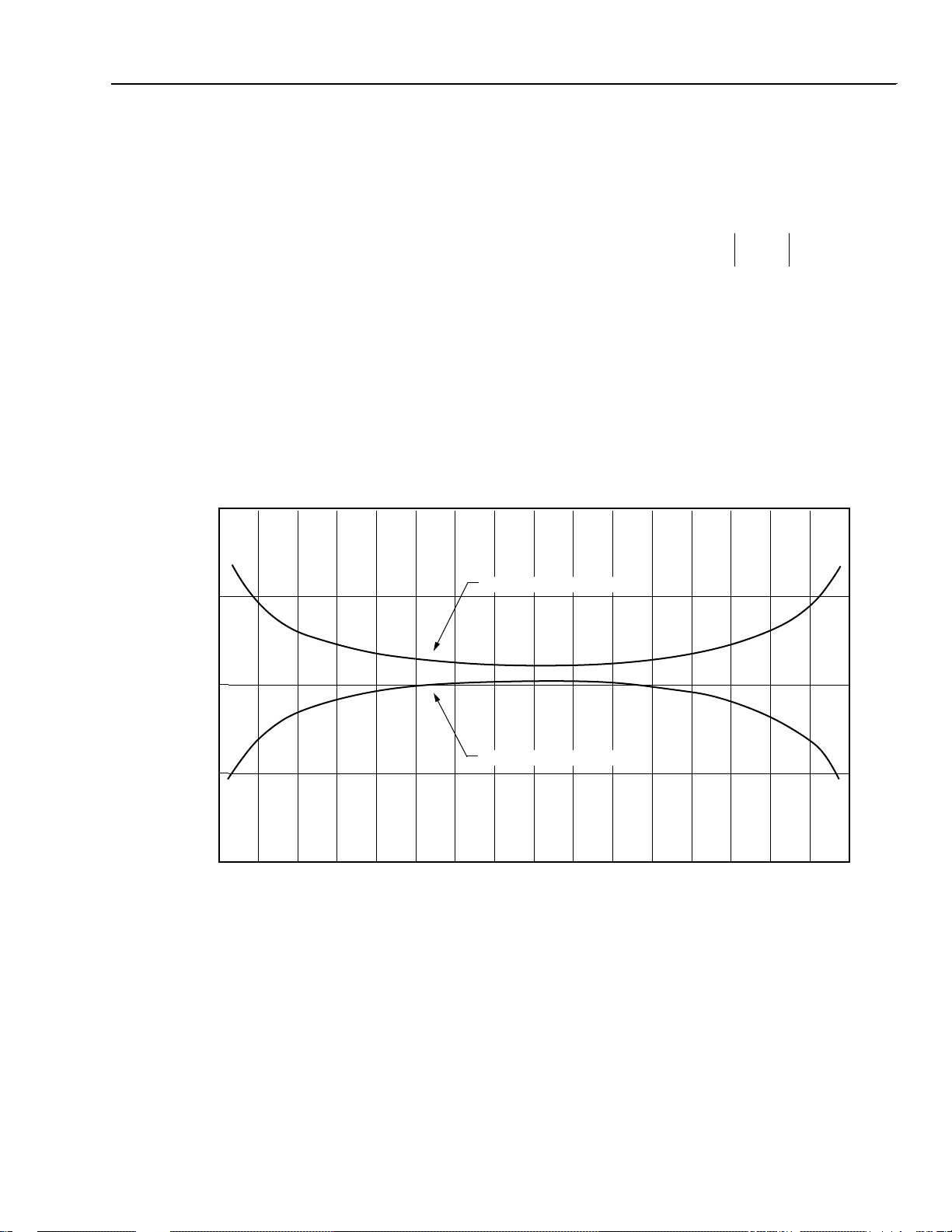
Data Sheet
February 1998 T7237 ISDN U-Interface Transceiver
Questions and Answers (continued)
U-Interface (continued)
Q12: I am planning on using a Raychem PTC (p/n
TR600-150) on the U-interface of the T7237 as
shown in Figure 17. The device is rated at 6 Ω—
12 Ω. I am concerned about the loose tolerance
on the PTC resistance. Will I be able to pass the
return loss requirements in ANSI T1.601 Section
7.1?
A12: The NT1 impedance limits looking into tip/ring are
derived from the T1.601 return loss requirements
(Figure 14 in T1.601). At the narrowest point in
the templates, the permissible range is between
111 Ω to 165 Ω. The tolerance on the PTC will
reduce the impedance margin somewhat, but
should still be acceptable.
10000
Figure 26 is derived from the return loss template
in ANSI T1.601. Return loss is a measure of the
match between two impedances on either side of
a junction point. The following equation is an
expression of return loss in terms of the complex
impedances of the two halves of the circuit Z
Z
1 Z2+
RL (dB) = 20 log
------------------ -
1 Z2–
Z
1, Z2.
When the impedances are not matched, the junction becomes a reflection point. For a perfectly
matched load, the return loss is infinite, whereas
for an open or short circuit, the return loss is zero.
The return loss expresses the ratio of incident to
reflected signal power and should consequently
be fairly high.
1000
100
IMPEDANCE (Ω)
10
1
1.0 1.4 2.0 2.8 4.0 5.6 7.9 11.2 15.8 22.4 31.6 44.7 63.1 89.1 125.9 177.8 251.2
UPPER BOUND > 165 Ω
LOWER BOUND < 110.4 Ω
FREQUENCY (kHz)
5-4056 (C)
Figure 26. Transceiver Impedance Limits
Lucent Technologies Inc. 57

Data Sheet
T7237 ISDN U-Interface Transceiver February 1998
Questions and Answers (continued)
U-Interface (continued)
A12: (continued)
It is desirable to express the return loss in terms of
impedance bounds, since an impedance measurement is relatively simple to make. From the
above equation, upper and lower bounds on impedance magnitude can be derived as follows:
O = return loss reference impedance = 135 Ω
Z
ZU = upper impedance curve
ZL = lower impedance curve
Upper bound (ZU > ZO):
ZO ZU+
L < ZO):
1+
1–
1–
1+
--------------------
U ZO–
Z
Z O Z L+
------------------- -
U ZL–
Z
O
Z
==
O
Z
==
---------- -
110
+
------------------------- -
---------- -
110
110
-------------------------- 110
20
–
L:
---------- -
–
---------- -
+
RL–
20
RL–
RL–
20
RL–
20
RL (dB) = 20 log
Lower bound (Z
RL (dB) = 20 log
Note that the higher the minimum return loss
requirement, the tighter the impedance limits will
be around Z
O, and vice versa.
So, for the upper bound, solve for ZU:
RL
------- -
20
Z U Z O
10
---------------------- -
RL
------- 20
10
For the lower bound, solve for Z
RL
------- -
20
ZUZO
10
------------------------
RL
------- 20
10
Plotting the above equations (using 135 for Zo
and Figure 13 in T1.601 f or the RL values) results
in the graph shown in Figure 26, which shows the
return loss expressed in terms of impedance
upper and lower bounds.
Q13: Why must secondary protection, such as a SGS-
Thomson SM6T6V8CA protection diode, be
used?
A13: The purpose of the diode is to protect against
metallic surges below the breakdown level of the
primary protector.
Such metallic surges can be coupled through the
transformer and could cause device damage if
the currents are high. The protector does not provide absolute protection for the device, but it
works in conjunction with the built-in protection
on the device leads.
The breakdown voltage level for secondary protection devices must be chosen to be above the
normal working voltage of the signal and typically
below the breakdown voltage level of the next
stage of protection. The SM6T6V8CA has a minimum breakdown voltage level of 6.4 V and a
maximum breakdown voltage of 7.1 V.
The chip pins that the SM6T6V8CA protects are
pins 36 (HP), 31 (HN), 32 (LOP), and 35 (LON).
The 16.9 Ω resistors will help to protect pins 32
and 35, but pins 31 and 36 will be directly
exposed to the voltage across the SM6T6V8CA.
The on-chip protection on these pins consists of
output diodes and a pair of polysilicon resistors.
These pins have been thoroughly tested to
ensure that a 7.1 V level will not damage them;
therefore, no third level of protection is needed
between the SM6T6V8CA and the HP and HN
pins.
The SM6T6V8CA has a maximum reverse surge
voltage level of 10.5 V at 57 A. Sustained currents this large on the device side of the transformer are not a concern in this application.
Thus, there should never be more than 7.1 V
across the SM6T6V8CA, except for possibly an
ESD or lightning hit. In these cases, the T7237 is
able to withstand at least ±1000 V (human-body
model) on its pins.
58 Lucent Technologies Inc.

Data Sheet
February 1998 T7237 ISDN U-Interface Transceiver
Questions and Answers (continued)
U-Interface (continued)
Q14: Where can information be obtained on lightning
and surge protection requirements for 2B1Q
products?
A14: Requirements vary among applications and
between countries. ANSI T1.601, Appendix B,
provides a list of applicable specifications to
which you may refer. Also, there are many manufacturers of overvoltage protection devices who
are familiar with the specifications and would be
willing to assist in surge protection design. The
ITU-T K series recommendations are also a good
source of information on protection, especially
recommendation K.11, “Principles of Protection
Against Overvoltages and Overcurrents,” which
presents an overview of protection principles.
Also refer to the application notes mentioned in
the U-interface Description section of this data
sheet.
Q15: ITU-T specification K.21 describes a lightning
surge test for NT1s (see Figure 1/K.21 and Table
1/K.21, Test #1) in which both tip and ring are
connected to the source and a 1.5 kV voltage
surge is applied between this point and the GND
of the NT1. What are the protection considerations for this test? Are the HP and HN pins susceptible to damage?
A15: The critical component in this test is the trans-
former since its breakdown voltage must be
greater than 1.5 kV. Assuming this is the case,
the only voltage that will make it through to the
secondary side of the transformer will be primarily due to the interwinding capacitance of the
transformer coils. This capacitance will look like
an impedance to the common-mode surge and
will therefore limit current on the device side of
the transformer. The device-side voltage will be
clamped by the SM6T6V8CA device. The maximum breakdown voltage of the SM6T6V8CA is
7.1 V. The 16.9 Ω resistors will help protect the
LOP and LON pins on the T7237 from this voltage. Howe v er , this voltage will be seen directly on
pins 36 and 31 (HP and HN) on the T7237. The
on-chip protection on these pins consists of output diodes and a pair of polysilicon resistors.
These pins have been thoroughly tested to
ensure that an 7.4 V level will not damage them;
therefore, no third level of protection is needed
between the SM6T6V8CA and the HP and HN
pins.
Q16: Can the range of the T7237 on the U-interface be
specified in terms of loss? What is the range over
straight 24 awg wire?
A16: ANSI Standard T1.601, Section 5.1, states that
transceivers meeting the U-interface standard are
intended to operate over cables up to the limits of
18 kft (5.5 km) 1300 Ω resistance design. Resistance design rules specify that a loop (of singleor mixed-gauge cable; e.g., 22 awg, 24 awg, and
26 awg) should have a maxim um dc resistance of
1300 Ω, a maxim um working length of 18 kft, and
a maximum total bridged tap length of 6 kft.
The standard states that, in terms of loss, this is
equivalent to a maximum insertion loss of 42 dB
@ 40 kHz. Lucent Technologies has found that,
for assessing the condition of actual loops in the
field in a 2B1Q system, specifying insertion loss
as 33.4 dB @ 20 kHz more closely models ANSI
circuit operation. This is equivalent to a straight
26 awg cable with 1300 Ω dc resistance
(15.6 kft).
The above goals are for actual loops in the outside loop plant. These loops may be subjected to
noise and jitter. In addition, as mentioned above,
there may be bridge taps at various points on the
loop. The T1.601 standard defines 15 loops, plus
the null, or 0-length loop, which are intended to
represent a generic cross section of the actual
loop plant.
A 2B1Q system must perform over all of these
loops in the presence of impairments with an
error rate of <1e–7. Loop #1 (18 kft, where
16.5 kft is 26 awg cable and 1.5 kft is 24 awg
cable) is the longest, so it has the most loss
(37.6 dB @ 20 kHz and 47.5 dB @ 40 kHz). Note
that this is more loss than discussed in the preceding paragraph. The diff erence is based on test
requirements vs. field deployment. The test
requirements are somewhat more stringent than
the field goal in order to provide some margin
against severe impairments, complex bridged
taps, etc.
Lucent Technologies Inc. 59

Data Sheet
T7237 ISDN U-Interface Transceiver February 1998
Questions and Answers (continued)
U-Interface (continued)
A16: (continued)
If a transceiver can operate over Loop #1 errorfree, it should have adequate range to meet all
the other loops specified in T1.601. Loop #1 has
no bridged taps, so passing Loop #1 does not
guarantee that a transceiver will successfully
start up on every loop. Also, due to the complex
nature of 2B1Q transceiver start-up algorithms,
there may be shorter loops which could cause
start-up problems if the transceiver algorithm is
not robust. The T7237 has been tested on all of
the ANSI loops per the T1.601 standard and
passes them all successfully. Two loops commonly used in the lab to evaluate the performance of the T7237 silicon are as follows:
Loop
Configuration
18 kft, 26 awg None 38.7 49.5
15 kft, 26 awg Two at
The T7237 is able to start up and operate errorfree on both of these loops. Neither of these
loops is specified in the ANSI standard, but both
are useful for evaluation purposes. The first loop
is used because it is simple to construct and easy
to emulate using a lumped parameter cable
model, and it is very similar to ANSI Loop #1, but
the loss is slightly worse. Thus, if a transceiver
can start up on this loop and operate error-free,
its range will be adequate to meet the longest
ANSI loop. The second loop is used because,
due to its difficult bridge tap structure and its
length, it stresses the transceiver start-up algorithms more than any of the ANSI-defined loops.
Therefore, if a transceiver can start up on this
loop, it should be able to meet any of the ANSIdefined loops that have bridge taps. Also, on a
straight 26 awg loop, the T7237 can successfully
Bridge
Taps (BT)
near end,
each 3 kft,
22 awg
Loss
@ 20
kHz
(dB)
37.1 46.5
Loss
@ 40
kHz
(dB)
start up at lengths up to 21 kft. This fact, combined with reliable start-up on the 15 kft 2BT loop
above, illustrates that the T7237 provides ample
start-up sensitivity, loop range, and robustness
on all ANSI loops. Another parameter of interest
is pulse height loss (PHL). PHL can be defined as
the loss in dB of the peak of a 2B1Q pulse relative to a 0-length loop. For an 18 kft 26 awg loop,
the PHL is about 36 dB, which is 2 dB worse than
on ANSI Loop #1. A signal-to-noise ratio (SNR)
measurement can be performed on the received
signal after all the signal processing is complete
(i.e., at the input to the slicer in the decision
feedback equalizer). This is a measure of the
ratio of the recovered 2B1Q pulse height vs.
the noise remaining on the signal. The SNR
must be greater than 22 dB in order to operate
with a bit error rate of <1e–7. With no impairments, the T7237 SNR is typically 32 dB on the
18 kft/26 awg loop. When all ANSI-specified
impairments are added, the SNR is about
22.7 dB, still leaving adequate margin to guarantee error-free operation over all ANSI loops.
Finally, to estimate range over straight 24 awg
cable, the 18 kft loop loss can be used as a limit
(since the T7237 can operate successfully with
that amount of loss) and the following calculations can be made:
Loss of 18 kft, 26 awg loop @ 20 kHz 38.7 dB
Loss per kft of 24 awg cable @ 20 kHz 1.6 dB
38.7 dB
--------------------------- - 24 kft=
1.6 dB
Thus, the operating range over 24 awg cable is
expected to be about 24 kft.
Q17: What does the energy spectrum of a 2B1Q signal
look like?
A17: Figure A1 (curve P1) in the ANSI T1.601 stan-
dard illustrates what this spectrum looks like.
/kft
60 Lucent Technologies Inc.

Data Sheet
February 1998 T7237 ISDN U-Interface Transceiver
Questions and Answers (continued)
U-Interface (continued)
Q18: Please clarify the meaning of ANSI Standard
T1.601, Section 7.4.2, Jitter Requirement #3.
A18: The intent of this requirement is to ensure that
after a deactivation and subsequent activation
attempt (warm-start), the phase of the receive
and transmit signals at the NT will be within the
specified limits relative to what they were prior to
deactivation. This is needed so that the LT, upon
a warm-start attempt, can make an accurate
assumption about the phase of the incoming NT
signal with respect to its transmit signal. Note that
the T7237 meets this requirement by design
because the NT phase offset from transmit to
receive is always fixed.
Q19: I need a way to generate a scrambled 2B1Q data
stream from the T7237 for test purposes (e.g.,
ANSI T1.601 Section 5.3.2.2, Total Power and
Section 7.2, Longitudinal Output Voltage). How
can I do this?
A19: A scrambled 2B1Q data stream (the SN1 signal
described in ANSI T1.601 Table 5) can be generated by pulling ILOSS
Q20: We are trying to do a return loss measurement on
the U-interface of the T7237 per ANSI T1.601
Section 7.1. We are using a circuit similar to the
one you recommend in the data sheet. We have
observed the following. When the chip is in FULL
RESET mode (powered on but no activity on the
U- or S/T-interfaces), the return loss is very low,
i.e., the termination impedance appears to be
very large relative to 135 Ω and falls outside the
boundaries of Figure 19 of ANSI T1.601. However, if we inject a 10 kHz tone before making a
measurement, the return loss falls within the template. Why is it necessary to inject the 10 kHz
tone in order to get this test to pass? Shouldn’t a
135 Ω impedance be presented to the network
regardless of the state of the T7237 once it is
powered on?
A20: The return loss is only relevant when the trans-
mitter section is powered on. When the transmitter is powered, it presents a low-impedance
output to the U-interface. The transmitter m ust be
held in this low-impedance state when the return
loss and longitudinal balance tests are performed. This can be accomplished by pulling
RESET low (pin 43). With the RESET pin held
low, the transmitter is held in a low-impedance
(pin 6) low on the T7237.
state where each of its differential outputs drives
DV. In this state, it is prevented from transmitting
any 2BIQ data and won’t respond to any incoming wakeup tones. This is different than the ANSIdefined FULL RESET state that the chip enters
after power-on or deactivation. In FULL RESET,
the transmitter is powered down and in a highimpedance state, with only the tone detector
powered on and looking for a far-end wakeup
tone. The transmitter powers down when in FULL
RESET state to save power and maximize the
tone detector sensitivity. The reason that the chip
behaves as it does in your tests is that your test
begins with the transmitter in its FULL RESET
state, causing the return loss to be very low. If a
10 kHz signal is applied, the tone detector
senses the applied signal and triggers. This
causes the transmitter to enter its low-impedance
state, where it will remain until the T7237 start-up
state machine times out (typically within 1.5 seconds, depending on the signal from the far end).
Q21: What are the average cold-start and warm-start
times?
A21: Lab measurements have shown the average
cold-start time to be about 3.3 s—4.2 s over all
loop lengths, and the average warm-start time to
be around 125 ms—190 ms over all loop lengths.
Q22: What is the U-interface’s response time to an
incoming wakeup tone from the LT?
A22: Response time is about 1 ms.
Q23: What is the minimum time for a U-interface
reframe after a momentary (<480 ms) loss of synchronization?
A23: Five superframes (60 ms).
Q24: Where is the U-interface loopback 2 (i.e., EOC
2B+D loopback) performed in the T7237?
A24: It is performed just inside the chip at the S/T-inter-
face. The S/T receiver is disconnected internally
from the chip pins, and the S/T transmit signal is
looped back to the receiver inputs so the S/T section synchronizes to its own signal. This ensures
that as much of the data path as possible is being
tested during the 2B+D loopback.
Q25: Are the embedded operations channel (EOC) ini-
tiated B1 and B2 channel loopbacks transparent?
A25: Yes, the B1 and B2 channel loopbacks are trans-
parent, as is the 2B+D loopback.
Lucent Technologies Inc. 61

Data Sheet
T7237 ISDN U-Interface Transceiver February 1998
Questions and Answers (continued)
U-Interface (continued)
Q26: How can proprietary messages be passed across
the U-interface?
A26: The embedded operations channel (EOC) pro-
vides one way of doing this. ANSI standard
T1.601 defines 64 8-bit messages which can be
used for nonstandard applications. They range in
value from binary 00010000 to 01000000.
There is also a provision for sending bulk data
over the EOC . Setting the data/message indicator
bit to 0 indicates the current 8-bit EOC word contains data that is to be passed transparently without being acted on. Note that there is no
response time requirement placed on the NT in
this case (i.e., the NT does not have to echo the
message back to the LT). Also note that this is
currently only an ANSI provision and is not an
ANSI requirement. The T7237 does support this
provision.
Q27: What is the value of the ANSI T1.601 cso and nib
bits in the 2B1Q frame?
A27: cso and nib are fixed at 0 and 1, respectively, by
the device. This is because the device alwa ys has
warm-start capability (CSO = 0), and NT1s are
required to have nib = 1 per T1.601-1992.
Q28: Are the PS bits controllable from outside the
chip?
A28: Yes, the bits are controlled by two pins (8 and 9)
on the chip. When the T7237 TDM highway is
enabled, these pins change function and become
part of the TDM highway and PS1 and PS2 are
controlled by register GR1, bits 1 and 2.
Q29: What is the state of the D-echo bit during an EOC
2B+D loopback?
A29: The D-echo bit (SXE, GR2, bit 3) should be set to
zero to meet the ITU-T I.430 requirement in
Appendix I, Note 4, which states that during a
loopback 2 (EOC 2B+D loopback), the NT1
should send INFO4 frames toward the TE with
the D-echo channel bits set to binary zero. If
AUTOEOC = 1 (register GR0, bit 4), SXE is internally overridden to 0 by the T7237. If AUTOEOC
= 0, SXE must be set to 0 by the user.
Miscellaneous
Q30: Is the ±100 ppm free-run frequency recommen-
dation met in the T7237?
A30: In the free-run mode, the output frequency is pri-
marily dependent on the crystal, not the silicon
design. For low-cost crystals, initial tolerance,
temperature, and aging effects may account for
two-thirds of this budget, and just a couple of pF
of variation in load capacitance will use up the
rest; therefore, the ±100 ppm goal can be met if
the crystal parameters are well controlled. See
the Crystal Characteristics section in this data
sheet.
Q31: What happens if Co and Cm of the crystal differs
from the specification shown in the Crystal Characteristics table?
A31: None of the parameters should be varied. We
have not characterized any such crystals, and
have no easy method of doing so. A crystal
whose parameters deviate from the requirements
may work in most applications but fail in isolated
cases involving certain loop configurations or
other system variations. Therefore, customers
choosing to vary any of these parameters do so
at their own risk.
Q32: It has been noted in some other designs that the
crystal has a capacitor from each pin to ground.
Changing these capacitances allows the frequency to be adjusted to compensate for board
parasitics. Can this be done with the T7237 crystal? Also, can we use a crystal from our own
manufacturer?
A32: For the T7237, these capacitors are located on
the chip, so their values are fixed. The advantage
to this is that no external components are
required. The disadvantage is that board parasitics must be very small.The crystal characteristics
section of the data sheet notes that the board
parasitics must be within the range of 0.6 pF ±
0.4 pF.
62 Lucent Technologies Inc.

Data Sheet
February 1998 T7237 ISDN U-Interface Transceiver
Questions and Answers (continued)
Miscellaneous (continued)
Q33: What clocks are available on the T7237?
A33: The following clocks are availab le and are always
present once enabled, regardless of the state of
activation on the U- or S/T-interfaces:
1. SYN8K, pin 4 (8 kHz clock) is enabled by holding SDI (pin 12) low during an external RESET.
2. TDMCLK, pin 9 (2.048 MHz clock) is enabled
by writing TDMEN = 0 (register GR2, bit 5).
3. CKOUT, pin 17 (10.24 MHz or 15.36 MHz
clock) is enabled by writing register GRO, bit 2
or 1, respectively, to 0. Normally 3-stated.
Note that using clocks 2 or 3 above requires a
microprocessor for setting the appropriate configuration.
Q34: I plan to program the T7237 to output 15.36 MHz
from its CKOUT pin. Is this clock a buffered version of the 15.36 MHz oscillator clock? I am concerned that if it is not buffered, the capacitive
loading on this pin could affect the system clock
frequency.
A34: The 15.36 MHz output is a buffered version of the
XTAL clock and therefore hanging capacitance
on it will not affect the T7237’s system clock frequency.
Q35: How does the filtering at the OPTOIN input work?
A35: The signals applied to OPTOIN are digitally fil-
tered for 20 ms. Any transitions under 20 ms will
be ignored.
Q36: What is the isolation voltage of the 6N139
optoisolator used in the dc termination circuit of
the T7237?
A36: 2500 Vac, 1 minute.
A38: The device’s reset is more dependent on the
RESET
As long as the proper input conditions on the
RESET pin (see Table 42) are met, the device will
have a valid reset. Note that this input is a
Schmitt-trigger input.
Q39: Is there a recommended method for powering the
T7237? For example, is it desirable to separate
the power supplies, etc.?
A39: The T7237 is not extremely sensitive to power-
supply schemes. Following standard practices of
decoupling power supplies close to the chip and,
if power and ground planes are not used, keeping
power traces away from high-frequency signals,
etc., should yield acceptable results. Separating
the T7237 analog power supplies from the digital
power supplies near the chip may yield a small
improvement, and the same holds true for using
power and ground planes vs. discrete traces.
Note that if analog and digital power supplies are
separated, the crystal power supply (V
should be tied to the digital supplies (VDDD).
See the SCNTI Family Reference Design Board
Hardware User Manual (MN96-011ISDN),
Appendix A for an example of a board layout that
performs well.
Q40: What are the filter characteristics of the PLL at
the NT?
A40: The –3 dB frequency is approximately 5 Hz,
peaking is about 1.2 dB.
Q41: Can you provide detailed information on the
active and idle power consumption of the T7237?
A41: The IDLE power of the T7237 is typically 35 mW.
The IDLE power will be increased if CKOUT or
the TDM highwa y is activ e . The discussion belo w
presents accurate numbers for adding in the
effects of CKOUT and the TDM highway.
pin than the power supply to the device.
DDO)
Q37: Can the T7237 operate with an external
15.36 MHz clock source instead of using a crys-
tal?
A37: Yes, by leaving X1 disconnected and driving X2
with an external CMOS-level oscillator.
Q38: What is the effect of ramping down the power-
supply voltage on the device? When will it provide
a valid reset? This condition can occur when a
line-powered NT1’s line cord is repeatedly
plugged in and removed and plugged in again
before the power supply has had enough time to
fully ramp-up.
Lucent Technologies Inc. 63

Data Sheet
T7237 ISDN U-Interface Transceiver February 1998
Questions and Answers (continued)
Miscellaneous (continued)
A41: (continued)
When considering active power measurement figures, it is important to note that the conditions
under which power measurements are made are
not always completely stated by 2B1Q IC vendors. For example, loop length is not typically
mentioned in the context of power dissipation, y et
power dissipation on a short loop is noticeably
greater than on a long loop. There are two reasons for the increased power dissipation at
shorter loop lengths:
1. The overall loop impedance is smaller, requiring a higher current to drive the loop.
2. The far-end transceiver is closer, requiring the
near-end transceiver to sink more far-end current in order to maintain a virtual ground at its
transmitter outputs.
The following lab measurements provide an
example of how power dissipation varies with
loop length for a specific T7237 with its
15.36 MHz CKOUT output disabled (see the fol-
lowing table for inf ormation on CK OUT). Note that
power dissipation on a 0-length loop (the worstcase loop) is about 35 mW higher than on a loop
of >3 kft length—a significant difference. Thus,
loop length needs to be considered when determining worst-case power numbers.
Table 34. Power Dissipation Variation
Loop Configuration Power (mW)
18 kft/26 awg 270
6 kft/26 awg 270
3 kft/26 awg 274
2 kft/26 awg 277
1 kft/26 awg 285
0.5 kft/26 awg 293
0 kft 305
135 Ω load, ILOSS or
LPBK active, no
far-end transceiver*
278
Also, in the case of the T7237, the use of the output clock CK OUT (pin 17) needs to be considered
since its influence on power dissipation is significant. Some applications may make use of this
clock, while others may leave it 3-stated. The
power dissipation of CKOUT is shown in Table
35.
Table 35. Power Dissipation of CKOUT
CKOUT
Frequency
(MHz)
15.36 21.3 11.0
10.24 17.7 9.1
The T7237 TDM highway, when active, can add
another 3 mW of power.
Therefore, it is apparent that the conditions under
which power is measured must be clearly specified. The methods Lucent has used to evaluate
typical and worst-case power consumption are
based on our commitment to provide our customers with accurate and reliable data. Measurements are performed as part of the factory test
procedure using automated test equipment.
Bench top tests are performed in actual T7237based systems to correlate the automated test
data with an actual implementation. A conservative margin is then added to the test results for
publication in our data sheets.
The following table provides power-consumption
data for several scenarios so that knowledgeable
customers can fairly compare transceiver solutions. A baseline scenario is presented in the
Case 1 column, and then adders are listed in the
Cases 2—5 columns to account for the worstcase condition listed in each column so that an
accurate worst-case figure can be determined
based on the conditions that are present in a particular application. Note that the tests w ere run at
5 V, so changes in the supply voltage will change
the power accordingly.
Power Due to
CKOUT 40 pF
Load (mW)
Power Due to
CKOUT No
Load (mW)
* This is the configuration used by some IC manufacturers.
64 Lucent Technologies Inc.

Data Sheet
February 1998 T7237 ISDN U-Interface Transceiver
Questions and Answers (continued)
Miscellaneous (continued)
A41: (continued)
Table 36. Power Consumption
Variables Baseline Adders
Case 1 Case 2 Case 3 Case 4 Case 5
Loop Configuration >3 kft, 26 awg 0 kft* — — —
CKOUT, MHz (40 pF load)
Temperature (°C) 25 — — 85 —
TDM Highway Inactive — — — Active
Typical Power Consumption (mW) 254 35 22 5 3
* Some 2B1Q silicon vendors specify power using a configuration in which the IC is active and transmitting into a 135 Ω termination, with
no far-end transmitter attached. This configuration would cause an increase of 9 mW over the Case 1 column, instead of the 35 mW
shown here. This highlights the importance of specifying measurement conditions accurately when making comparisons between chip
vendors' power numbers.
† See the preceding table for a comparison of power dissipation with negligible capacitive loading on CKOUT. The 40 pF figure chosen
here is intended to represent a worst-case condition.
†
3-stated — 15.36 — —
Q42: The STLED on my T7237-based NT1 behaves in
an unexpected way. When a start-up attempt is
received, it flashes at an 8 Hz rate. Then it
flashes briefly at 1 Hz, indicating synchronization
on the U-interface. This is expected. However,
after this, it starts flashing at 8 Hz, and yet it
appears as though the system is operating fine
(data is being passed end to end, etc.). Shouldn’t
the STLED signal be always low (i.e., ON) at this
point?
A42: Yes it should. Referring to the STLED Control
Flow diagram in Figure 15 of this data sheet, it
appears as though you may be receiving aib = 0
from the upstream U-interface element. This will
cause the behavior you are seeing. If you have
access to the microprocessor registers, you can
check this by monitoring register CFR1 bit 6 to
see if it ever goes to 0.
Q43: We are testing out T7237-based equipment
against an Lucent SLC Series 5, and performance seems OK except that we get a burst of
errors, and even drop calls, approximately every
15 minutes. Can you explain why?
A43: Check to make sure that your equipment is set-
ting the PS1/PS2 power status bits correctly. The
SLC equipment monitors the PS1/PS2 bits and, if
they are both zero (meaning all power is lost), it
assumes that there is some sort of terminal error,
since this is not an appropriate steady-state value
for PS1/PS2. When this condition is detected, the
SLC deactivates and reactivates the line approximately every 15 minutes. This causes the symptoms you describe.
Lucent Technologies Inc. 65

Data Sheet
T7237 ISDN U-Interface Transceiver February 1998
Questions and Answers (continued)
Miscellaneous (continued)
Q44: What is the state of the T7237 TDM bus output
when the unused bits of the D-channel octet are
transmitted?
A44: The T7237 3-states the TDM bus output when B-
and D-channel information is not transmitted to
the TDM bus. This includes the 6-bit interval in
the D-channel octet.
Q45: What is the purpose of the ACTSEL bit in register
GR2 bit 6?
A45: This bit is to provide compatibility with the ANSI
T1.601 and ETSI ETR 080 standards. The 1992
version of T1.601 (the most recent as of this writing) specifies that, upon a loopback 2 EOC
request, the NT1’s 2B+D data should be looped
back immediately and the upstream (NT-to-LT)
act bit should be set to 0. ANSI specified that the
upstream act bit should be set to 0 to indicate to
the LT that end-to-end data transparency (TE-toLT) is interrupted during a loopback 2. The fact
that 2B+D data is looped back immediately
means that upstream data transparency at the
NT is established independent of the status of the
act bit from the LT. Normally, upstream data
transparency at the NT is dependent on act = 1
being received from the LT. The reason that loopback 2 transparency criteria differ is that there is
no guarantee that the NT1 will receive act = 1
from the LT. Consider the case where an LT
wants to activate the U-interface and perform a
loopback 2 test on an NT1 with no TE connected.
In this case, the LT will never receive act = 1
since, prior to the loopback 2 request, act = 0
because there is no TE attached, and after the
loopback 2 request, act = 0 because layer 1
transparency is interrupted. Since the LT will
never receive act = 1 from the NT1, it will never
send act = 1 back to the NT1. Since the NT1
receipt of act = 1 normally enables upstream
transparency, ANSI chose to make an exception
to the data transparency requirements in this
case and enable upstream transparency immediately upon receipt of the loopback 2 EOC command at the NT1.
The major difference between the ANSI and ETSI
standards with regard to how the NT1 handles a
loopback 2 request lies in what happens to the
upstream act bit. ANSI’s position is that act
should be set to 0 because a loopback 2 is an
interruption to layer 1 transparency. ETSI’s position is that the state of the act bit should only be
dependent on whether or not the NT1 is receiving
INFO 3 from the TE (this is consistent with ANSI
T1.601 paragraph 6.4.6.4 and ETSI ETR 080
paragraph A.10.1.5.1). During a loopback 2, the
T7237 will always receiv e INFO 3 at the S/T-interface (even if there is no TE attached) because it
loops back its S/T transmit signal and synchronizes itself to that signal. Therefore , the possibility
that LT will never receive act = 1 from the NT
does not exist under these rules. As a result, no
special exceptions need to be applied to the case
of loopback 2 in ETSI. For example, again consider the case where an LT wants to activate the
U-interface and perform a loopback 2 test on an
NT1 with no TE connected. The NT1 will synchronize to its own S/T signal and detect INFO 3. This
will cause act = 1 to be transmitted upstream. The
L T will detect act = 1 and set its do wnstream act =
1. When the NT detects the downstream act = 1,
it will enable upstream data transparency. The
handling of the act bit and transparency in this
case is the same as for a normal activation.
In the ETSI standard, transparency at the NT during loopback 2 is dependent upon the reception
of the act bit from the LT, i.e., if act = 1, loopback
transparency is established, and if act = 0, loopback data is forced to all 1s. The LT won’t send
act = 1 until it receives act = 1 from the NT. The
NT will not send act = 1 to the LT until it receives
an INFO 3 indication (i.e., until its S/T-interface is
synchronized as described in the register GR2
ACTSEL bit definition). Thus, data transparency
requires that the NT1 set its upstream act bit to 1.
There is a contribution that has been voted onto
the ANSI T1E1.4 living list that changes the act
bit behavior during loopback 2 to match that
specified for ETSI (contribution #T1E1.4/92-089).
Thus, the next issue of the T1.601 standard will
bring the ANSI and ETSI standards into harmony
as pertains to handling of the act bit during a
loopback 2.
66 Lucent Technologies Inc.

Data Sheet
February 1998 T7237 ISDN U-Interface Transceiver
Glossary
ACTMODE/INT: Act bit mode, serial interface
microprocessor interrupt.
ACTR: Receive activation
register CFR1, bit 0).
ACTSC: Activation/deactivation state
change on U-interface
(register UIR0, bit 1).
ACTSCM: Activation/deactivation state
change on U-interface interrupt
mask (register UIR1, bit 1).
ACTSEL: Act mode select (register
GR2, bit 6).
ACTT: Transmit activation (register
GR1, bit 4).
AFRST: Adaptive filter reset (register
CFR0, bit 1).
AIB: Alarm indication bit (register
CFR1, bit 6).
ANSI: American National Standards In-
stitute.
ASI: Alternate space inversion.
AUTOACT: Automatic activation control
(register GR0, bit 6).
AUTOCTL: Auto control enable
(register GR0, bit 3).
AUTOEOC: Automatic EOC processor
enable (register GR0, bit 4).
A[3:1]R: Receive EOC address (register
ECR2, bits 0—2).
A[3:1]T: Transmit EOC address
(register ECR0, bits 0—2).
BERR: Block error on U-interface
(register UIR0, bit 2).
BERRM: Block error on U-interface inter-
rupt mask (register UIR1, bit 2).
CCRC: Corrupt cyclic redundancy check
(register ECR0, bit 7).
CDM: Charged-device model.
CFR0: Control flow state machine con-
trol—maintenance/reserved bits
register.
CFR1: Control flow state machine status
register.
CFR2: Control flow state machine
status—reserved bits register.
CKOUT: Clock output.
CODEC: Coder/decoder, typically used for
analog-to-digital conversions or
digital-to-analog conversions.
CRATE[1:0]: CKOUT rate control (register
GR0, bits 2—1).
CRC: Cyclic redundancy check.
DFR0: Data flow control—U and S/T
B-channels register.
DFR1: Data flow control—D-channels
and TDM bus register.
DMR: Receive EOC data or message in-
dicator (register ECR2, bit 3).
DMT: Transmit EOC data or message
indicator (register ECR0, bit 3).
DPGS: Digital pair gain system.
ECR0: EOC state machine control—ad-
dress register.
ECR2: EOC state machine status—ad-
dress register.
ECR3: EOC state machine status—infor-
mation register.
EMINT: Exit maintenance mode interrupt
(register MIR0, bit 2).
EMINTM: Exit maintenance mode interrupt
mask (register MIR1, bit 2).
EOC: Embedded operations channel.
EOCSC: EOC state change on U-interface
(register UIR0, bit 0).
EOCSCM: EOC state change on U-interface
mask (register UIR1, bit 0).
ERC1: EOC state machine control—
information register.
Lucent Technologies Inc. 67

Data Sheet
T7237 ISDN U-Interface Transceiver February 1998
Glossary (continued)
ESD: Electrostatic discharge.
ETSI: European Telecommunications
Standards Institute.
FEBE: Far-end block error (register
CFR1, bit 5).
FSC[2:0]: Frame strobe (FS) control,
(register TDR0, bits 2—0).
FSP: Frame strobe (FS) polarity
(register TDR0, bit 3).
FT: Fixed/adaptive timing control
(register GR2, bit 0).
FTE/TDMDI: Fixed/adaptive timing mode
select.
GIR0: Global interrupt register.
A: Analog ground.
GND
GNDO: Crystal oscillator ground.
GR0: Global device control—device
configuration register.
GR1: Global device control—
U-interface register.
GR2: Global device control—
S/T-interface register.
HBM: Human-body model.
HDLC: High-level data link control.
HIGHZ: High-impedance control.
HN: Hybrid negative input for
U-interface.
HP: Hybrid positive input for
U-interface.
I4C: INFO 4 change (register SIR0,
bit 3).
I4CM: INFO 4 change mask (register
SIR1, bit 3).
I4I: INFO 4 indicator (register CFR1,
bit 7).
ILINT: Insertion loss interrupt
(register MIR0, bit 1).
ILINTM: Insertion loss interrupt mask
(register MIR1, bit 1).
ILOSS: Insertion loss test control
(register CFR0, bit 0).
ILOSS
ISDN: Integrated services digital net-
ITU-T: International Telecommunication
I[8:1]R: Receive EOC information
I[8:1]T: Transmit EOC information
LON: Line driver negative output for
LOP: Line driver positive output for
LPBK: U-interface analog loopback
MCR0: Q-channel bits register.
MCR1: S subchannel 1 register.
MCR2: S subchannel 2 register.
MCR3: S subchannel 3 register.
MCR4: S subchannel 4 register.
MCR5: S subchannel 5 register.
MINT: Maintenance interrupt
MIR0: Maintenance interrupt register.
MIR1: Maintenance interrupt mask
MLT: Metallic loop termination.
MULTIF: Multiframing control (register
NEBE: Near-end block error (register
NTM: NT test mode (register GR1, bit 3).
OOF: Out of frame (register CFR1,
OPTOIN: Optoisolator input.
OUSC: Other U-interface state change
: Insertion loss test control.
work.
Union-Telecommunication Sector.
(register ECR3, bits 0—7).
(register ERC1, bits 0—7).
U-interface.
U-interface.
(register GR1, bit 0).
(register GIR0, bit 2).
register.
GR0, bit 5).
CFR1, bit 4).
bit 2).
(register UIR0, bit 3).
68 Lucent Technologies Inc.

Data Sheet
February 1998 T7237 ISDN U-Interface Transceiver
Glossary (continued)
OUSCM: Other U-interface state change
mask (register UIR1, bit 3).
PS1: Power status #1 (register GR1,
bit 2).
PS1E/TDMDO: Power status #1, TDM clock.
PS2: Power status #2 (register GR1,
bit 1).
PS2E/TDMCLK: Power status #2, TDM data out.
QMINT: Quiet mode interrupt (register
MIR0, bit 0).
QMINTM: Quiet mode interrupt mask
(register MIR1, bit 0).
QSC: Q-bits state change (register
SIR0, bit 1).
QSCM: Q-bits state change mask
(register SIR1, bit 1).
Q[4:1]: Q-channel bits (register MCR0,
bits 0—3).
R25R: Receive reserved bits
(register CFR2, bit 2).
R25T: Transmit reserved bit
(register CFR0, bit 4).
R64T: Transmit reserved bit
(register CFR0, bit 5).
RESET
RNR: Receive negative rail for
RPR: Receive positive rail for
RSFINT: Receive superframe interrupt
RSFINTM: Receive superframe interrupt
R[16:15]R: Receive reserved bits
R[16:15]T: Transmit reserved bits
R[64:54:44:34]R: Receive reserved bits
: Reset.
S/T-interface.
S/T-interface.
(register UIR0, bit 4).
mask (register UIR1, bit 4).
(register CFR2, bits 1—0).
(register CFR0, bits 3—2).
(register CFR2, bits 6—3).
SAI[1:0]: S/T-interface activity indicator
control (register GR1, bits 6—7).
SC1[4:1]: S subchannel 1 (register MCR1,
bits 0—3).
SC2[4:1]: S subchannel 2 (register MCR2,
bits 0—3).
SC3[4:1]: S subchannel 3 (register MCR3,
bits 0—3).
SC4[4:1]: S subchannel 4 (register MCR4,
bits 0—3).
SC5[4:1]: S subchannel 5 (register MCR5,
bits 0—3).
SCK: Serial interface clock.
SDI: Serial interface data input.
SDINN: Sigma-delta A/D negative input
for U-interface.
SDINP: Sigma-delta A/D positive input for
U-interface.
SDO: Serial interface data output.
SFECV: S channel far-end code violation
(register SIR0, bit 2).
SFECVM: S subchannel far-end code viola-
tion mask (register SIR1, bit 2).
SINT: S/T transceiver interrupt
(register GIR0, bit 1).
SIR0: S/T-interface interrupt register.
SIR1: S/T-interface interrupt mask
register.
SOM: Start of multiframe (register SIR0,
bit 0).
SOMM: Start of multiframe mask
(register SIR1, bit 0).
SPWRUD: S/T-interface powerdown control
(register GR2, bit 1).
SRESET: S/T-interface reset (register GR2,
bit 2).
STLED: Status LED driver.
STOA: S/T-only activation (register GR2,
bit 7).
Superframe: Eight U-frames grouped together.
Lucent Technologies Inc. 69

Data Sheet
T7237 ISDN U-Interface Transceiver February 1998
Glossary (continued)
SXB1[1:0]: S/T-interface transmit path source
for B1 channel (register DFR0,
bits 5—4).
SXB2[1:0]: S/T-interface transmit path source
for B2 channel (register DFR0,
bits 7—6).
SXD: S/T-interface transmit path source
for D channel (register DFR1, bit
1).
SXE: S/T-interface D-channel echo bit
control (register GR2, bit 3).
SYN8K/LBIND/FS: Synchronous 8 kHz clock or loop-
back indicator, frame strobe.
TDM: Time-division multiplexed.
TDMB1S: TDM bus transmit control for
B1 channel from S/T-interface
(register DFR1, bit 2).
TDMB1U: TDM bus transmit control for
B1 channel from U-interface
(register DFR1, bit 5).
TDMB2S: TDM bus transmit control for B2
channel from S/T-interface
(register DFR1, bit 3).
TDMB2U: TDM bus transmit control for B2
channel from U-interface
(register DFR1, bit 6).
TDMDS: TDM bus transmit control for D
channel from S/T-interface
(register DFR1, bit 4).
TDMDU: TDM bus transmit control for D
channel from U-interface
(register DFR1, bit 7).
TDMEN: TDM bus select (register GR2,
bit 5).
TDR0: TDM bus timing control register.
TNR: Transmit negative rail for
S/T-interface.
TPR: Transmit positive rail for
S/T-interface.
TSFINT: Transmit superframe interrupt
(register UIR0, bit 5).
TSFINTM: Transmit superframe interrupt
mask (register UIR1, bit 5).
U frame: An 18-bit synchronous word.
U2BDLN: Nontransparent 2B+D loopback
control (register GR2, bit 4).
U2BDLT: Transparent 2B+D loopback con-
trol (register ECR0, bit 6).
UB1LP: U-interface loopback of B1 chan-
nel control (register ECR0, bit 4).
UB2LP: U-interface loopback of B2 chan-
nel control (register ECR0, bit 5).
UINT: U transceiver interrupt (register
GIR0, bit 0).
UIR0: U-interface interrupt register.
UIR1: U-interface interrupt mask
register.
UOA: U-interface only activation,
(register CFR1, bit 3).
UXB1[1:0]: U-interface transmit path source
for B1 channel (register DFR0,
bits 1—0).
UXB2[1:0]: U-interface transmit path source
for B2 channel (register DFR0,
bits 3—2).
UXD: U-interface transmit path source
for D channel (register DFR1,
bit 0).
DDA: Analog power.
V
VDDO: Crystal oscillator power.
VRCM: Common-mode voltage reference
for U-interface circuits.
VRN: Negative voltage reference for U-
interface circuits.
VRP: Positive voltage reference for U-
interface circuits.
X1: Crystal #1.
X2: Crystal #2.
XACT: U transceiver active (register
CFR1, bit 1).
XPCY: Transparency (register GR1,
bit 5).
70 Lucent Technologies Inc.

Data Sheet
February 1998 T7237 ISDN U-Interface Transceiver
Standards Documentation
Telecommunication technical standards and reference
documentation may be obtained from the following
organizations:
ANSI (U.S.A.):
American National Standards Institute (ANSI)
11 West 42nd Street
New York, New Y ork 10036
T el: 212-642-4900
F AX: 212-302-1286
Lucent Tec hnologies Publications:
Lucent Technologies Customer Information Center
(CIC)
Tel: 800-432-6600
FAX: 800-566-9568 (in U.S.A.)
FAX: 317-322-6484 (outside U.S.A.)
Bellcore (U.S.A.):
Bellcore Customer Service
8 Corporate Plaza
Piscataway, New Jersey 08854
ITU-T:
International T elecommunication UnionTelecommunication Sector
Place des Nations
CH 1211
Geneve 20, Switzerland
Tel: 41-22-730-5285
FAX: 41-22-730-5991
ETSI:
European Telecommunications Standards Institute
BP 152
F-06561 Valbonne Cedex, France
Tel: 33-92-94-42-00
FAX: 33-93-65-47-16
TTC (Japan):
TTC Standard Publishing Group of the
Telecommunications Technology Committee
2nd Floor, Hamamatsucho-Suzuki Building,
1 2-11, Hamamatsu-cho, Minato-ku, Tokyo
Tel: 81-3-3432-1551
FAX: 81-3-3432-1553
Tel: 800-521-CORE (in U.S.A.)
Tel: 908-699-5800
FAX: 212-302-128
Lucent Technologies Inc. 71

For additional information, contact your Microelectronics Group Account Manager or the following:
INTERNET: http://www.lucent.com/micro
E-MAIL: docmaster@micro.lucent.com
U.S.A.: Microelectronics Group, Lucent Technologies Inc., 555 Union Boulevard, Room 30L-15P-BA, Allentown, PA 18103
1-800-372-2447, FAX 610-712-4106 (In CANADA: 1-800-553-2448, FAX 610-712-4106)
ASIA PACIFIC: Microelectronics Group, Lucent Technologies Singapore Pte. Ltd., 77 Science Park Drive, #03-18 Cintech III, Singapore 118256
Tel. (65) 778 8833, FAX (65) 777 7495
JAPAN: Microelectronics Group, Lucent Technologies Japan Ltd., 7-18, Higashi-Gotanda 2-chome, Shinagawa-ku, Tokyo 141, Japan
Tel. (81) 3 5421 1600, FAX (81) 3 5421 1700
EUROPE: Data Requests: MICROELECTRONICS GROUP DATALINE: Tel. (44) 1189 324 299, FAX (44) 1189 328 148
Technical Inquiries: GERMANY: (49) 89 95086 0 (Munich), UNITED KINGDOM: (44) 1344 865 900 (Bracknell),
FRANCE: (33) 1 41 45 77 00 (Paris), SWEDEN: (46) 8 600 7070 (Stockholm), FINLAND: (358) 9 4354 2800 (Helsinki),
ITALY: (39) 2 6601 1800 (Milan), SPAIN: (34) 1 807 1441 (Madrid)
Lucent Technologies Inc. reserves the right to make changes to the product(s) or information contained herein without notice. No liability is assumed as a result of their use or application. No
rights under any patent accompany the sale of any such product(s) or information.
Copyright © February 1998 Lucent Technologies Inc.
All Rights Reserved
Printed in U.S.A.
February 1998
DS97-411ISDN (Replaces DS96-041ISDN)
Printed On
Recycled Paper
 Loading...