LSI RDD104, RDD104-S Datasheet

SELECTABLE 4 DECADE CMOS DIVIDER
FEATURES:
• Selectable Divide by 10 or 100 or 1,000 or 10,000
• Clock Input Shaping Network Accepts Fast or Slow
Edge Inputs
• Active Oscillator Network for External Crystal
• Square Wave Output
• Output TTL Compatible at +4.5 Volt Operation
• High Noise Immunity
• Reset
• All Inputs Protected
• +4.5V to +15V Operation (VDD-VSS)
• Low Power Dissipaton
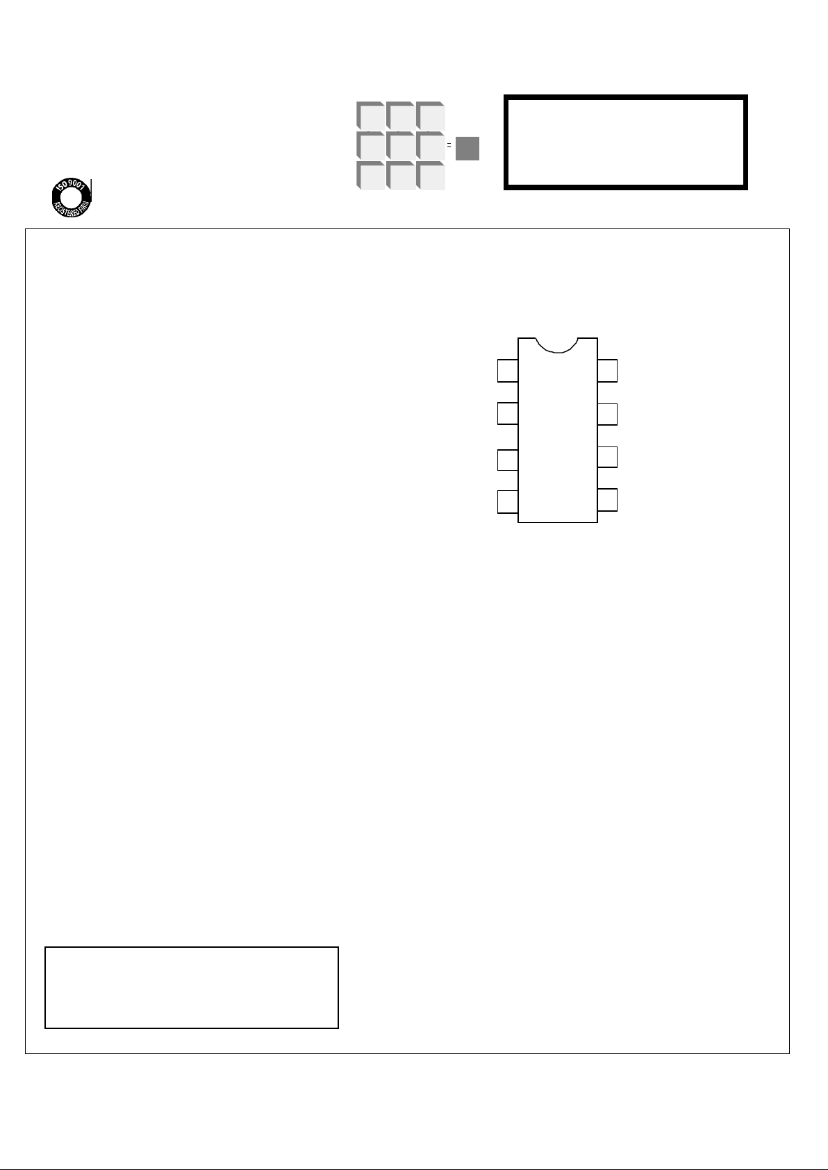
• RDD104 (DIP); RDD104-S (SOIC) - See Figure 1
DC ELECTRICAL CHARACTERISTICS:
(All voltages referenced to V
ss)
VDD
-40°C +25°C +85°C UNIT
Quiescent Device Current 4.5V 10 10 300 uA Max
10V 20 20 600 uA Max
Output Voltage, Low Level 4.5V 0.01 0.01 0.05 V Min
10V 0.01 0.01 0.05 V Min
High Level 4.5V 4.49 4.49 4.45 V Max
10V 9.99 9.99 9.95 V Max
Input Noise Immunity 4.5V 1.3 1.3 1.3 V Min
(Low and High) 10V 3.0 3.0 3.0 V Min
Output Drive Current:
N-Channel Sink Current 4.5V 2.3 1.9 1.6 mA Min
(V
OUT
= Vss + 0.4V) 10V 5.0 4.0 3.5 mA Min
P-Channel Source Current 4.5V 1.1 0.95 0.8 mA Min
(V
OUT
= V
DD
- 1V) 10V 2.5 2.1 1.8 mA Min
Input Capacitance (any input) 5.0 pF Max
DESCRIPTION OF OPERATION:
The RDD104 is a monolithic CMOS four decade
divider circuit that advances on each negative
transition of the input clock pulse. When the reset
input is high the circuit is cleared to zero. The
clock input is applied to a three stage inverting
amplifier network whose output is brought out so
that an external crystal network can be used to
form an oscillator circuit. If the clock output is not
used,the amplifier acts as an input buffer. Two
select inputs are provided which enables the circuit
to divide by 10, 100, 1,000 or 10,000.
The Output Division is selected according to the
following truth table:
DIVIDER SELECT INPUTS: OUTPUT
SELECT 2 SELECT 1 DIVISION
0 0 10,000
0 1 1,000
1 0 100
1 1 10
MAXIMUM RATINGS:
PARAMETER SYMBOL VALUE UNIT
Storage Temperature TSTG -65 to +150 °C
Operating Temperature TA -40 to +85 °C
DC Supply Voltage (VDD - VSS) +18 V
Voltage at any input VIN VSS - 0.5 to VDD + 0.5 V
January 2000
PIN ASSIGNMENT - TOP VIEW
1
2
3
4
5
6
7
8
LSI
FIGURE 1
VDD (+V)
OUTPUT
CLOCK OUTPUT
CLOCK INPUT
DIVIDER
SELECT-1
DIVIDER
SELECT-2
VSS (-V)
RESET
RDD 104
The information included herein is believed to be
accurate and reliable. However, LSI Computer Systems,
Inc. assumes no responsibilities for inaccuracies, nor for
any infringements of patent rights of others which may
result from its use.
RDD104-092491
LSI/CSI
LSI Computer Systems, Inc. 1235 Walt Whitman Road, Melville, NY 11747 (631) 271-0400 FAX (631) 271-0405
RDD 104
U
L
®
A3800

DYNAMIC ELECTRICAL CHARACTERISTICS:
(CL = 50pF, Input Rise and Fall Times = 20ns except for Clock,
unless otherwise specified.)
VDD MIN MAX UNIT
Clock Input Frequency 4.5V 0 1.5 MHz
10V 0 4.0 MHz
15V 0 6.0 MHz
Clock Input Rise & Fall Times 4.5 to 15V - No Limit
Clock Input Rise & Fall Time, 4.5V - 140 ns
CL = 15pF 10V - 70 ns
Clock Output Propagation 4.5V - 300 ns
Delay, CL = 15pF 10V - 150 ns
Output Rise & Fall Times 4.5V - 400 ns
10V - 200 ns
Propagation Delay to Output 4.5V - 1500 ns
10V - 750 ns
Reset Pulse Width 4.5V 800 - ns
10V 400 - ns
Reset Removal Time 4.5V - 500 ns
10V - 250 ns
Reset Propagation Delay 4.5V - 1400 ns
to Output 10V - 700 ns
Select Input Setup Time 4.5V - 800 ns
10V - 400 ns
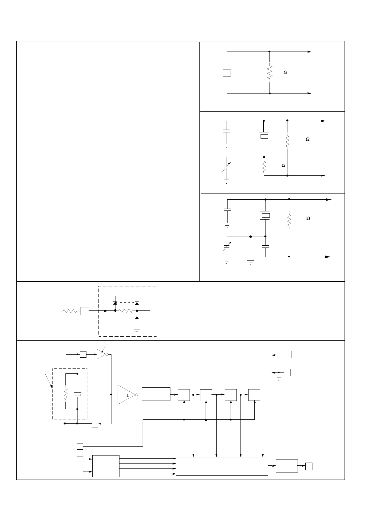
MINIMUM PARTS OSCILLATOR CIRCUIT
PIN 6
10M
PIN 5
FIGURE 2.
TYPICAL OSCILLATOR CIRCUIT WITH TRIM -1 MHZ AND BELOW
PIN 5
PIN 6
20M
10M
100pF
40pF
FIGURE 3.
PIN 5
PIN 6
39pF
10M
FIGURE 4.
TYPICAL OSCILLATOR CIRCUIT WITH TRIM - ABOVE 1 MHZ
56pF
50pF
20pF
CLOCK
INPUT
SIGNAL
R1
VSS
VDD VDD
5
FIGURE 5. TYPICAL INPUT
If input signals are less than VSS or greater than
VDD, a series input resistor, R1, should be used to
limit the maximum input current to 2 milliamperes.
BUFFER
+V
-V
1 OUT OF 4 SELECTOR
DECODER
8
3
7
5
4
1
2
FIGURE 6.
RDD 104 BLOCK DIAGRAM
CLOCK
GENERATOR
÷ ÷ ÷ ÷
10 10 10 10
R
CLOCK IN
CLOCK OUT
RESET
DIVIDER SELECT-1
DIVIDER SELECT-2
6
OSCILLATOR
EXTERNAL
COMPONENTS
OUTPUT
VDD
VSS
3 STAGE INVERTING
AMPLIFIER
RDD104-011000-2
 Loading...