

Page 1

Technical
Manual
LSIFC929DualChannel
Fibre Channel I/O
Processor
Revision 2.0
August 2001
®
S14073
Page 2

Electromagnetic Compatibility Notices
This device complies with Part 15 of the FCC Rules. Operation is subject to the following two conditions:
1. This device may not cause harmful interference, and
2. This device must accept any interference received, including interference that may cause undesired operation.
This equipment has been tested and found to comply with the limits for a Class B digital device, pursuant to part 15
of the FCC Rules. These limits are designed to provide reasonable protection against harmful interference in a
residential installation. This equipment generates, uses, and can radiate radio frequency energy and, if not installed
and used in accordance with the instructions, may cause harmful interference to radio communications. However,
there is no guaranteethat interference will not occur in a particular installation. If this equipment does cause harmful
interference to radio or television reception, which can be determined by turning the equipment off and on, the user
is encouraged to try to correct the interference by one or more of the following measures:
• Reorient or relocate the receiving antenna.
• Increase the separation between the equipment and the receiver.
• Connect the equipment into an outlet on a circuit different from that to which the receiver is connected.
• Consult the dealer or an experienced radio/TV technician for help.
Shielded cables for SCSI connection external to the cabinet are used in the compliance testing of this Product.
LSI Logic is not responsible for any radio or television interference caused by unauthorized modification of this
equipment or the substitution or attachment of connecting cables and equipment other than those specified by
LSI Logic. The correction of interferences caused by such unauthorized modification, substitution, or attachment will
be the responsibility of the user.
The LSI Logic LSIFC929 is tested to comply with FCC standards for home or office use.
This Class B digital apparatus meets all requirements of the Canadian Interference-Causing Equipment Regulations.
Cet appareil numérique de la classe B respecte toutes les exigences du Règlement sur le matériel brouilleur du
Canada.
This is a Class B product based on the standard of the Voluntary Control Council for Interference from Information
Technology Equipment (VCCI). If this is used near a radio or television receiver in a domestic environment, it may
cause radio interference. Install and use the equipment according to the instruction manual.
LSI Logic Corporation
North American Headquarters
Milpitas, CA
408.433.8000
ii
Copyright © 2000, 2001 by LSI Logic Corporation. All rights reserved.
Page 3

This document is preliminary. As such, it contains data derived from functional
simulations and performance estimates. LSI Logic has not verified either the
functional descriptions, or the electrical and mechanical specifications using
production parts.
This document contains proprietary information of LSI Logic Corporation. The
information contained herein is not to be used by or disclosed to third parties
LSI Logic products are not intended for use in life-support appliances, devices,
or systems. Use of any LSI Logic product in such applications without written
consent of the appropriate LSI Logic officer is prohibited.
DB14-000135-02, Third Edition (August 2001)
This document describes LSI Logic Corporation’s LSIFC929 Dual Channel Fibre
Channel I/O Processor and will remain the official reference source for all
revisions/releases of this product until rescinded by an update.
LSI Logic Corporation reserves the right to make changes to any products herein
at any time without notice. LSI Logic does not assume any responsibility or
liability arising out of the application or use of any product described herein,
except as expressly agreed to in writing by LSI Logic; nor does the purchase or
use of a product from LSI Logic convey a license under any patent rights,
copyrights, trademark rights, or any other of the intellectual property rights of
LSI Logic or third parties.
Copyright © 2000, 2001 by LSI Logic Corporation. All rights reserved.
TRADEMARK ACKNOWLEDGMENT
The LSI Logic logo design and GigaBlaze are registered trademarks of LSI Logic
Corporation. ARM is a registered trademark of ARM Ltd.,, used under license.
All other brand and product names may be trademarks of their respective
companies.
DB
To receive product literature, visit us at http://www.lsilogic.com.
For a current list of our distributors, sales offices, and design resource
centers, view our web page located at
http://www.lsilogic.com/contacts/na_salesoffices.html
Copyright © 2000, 2001 by LSI Logic Corporation. All rights reserved.
iii
Page 4

iv
Copyright © 2000, 2001 by LSI Logic Corporation. All rights reserved.
Page 5

Audience
Preface
This book is the primary reference and technical manual for the
LSIFC929 Fibre Channel I/O Processor. It contains a complete functional
description for the LSIFC929 and includes complete physical and
electrical specifications for the product.
This document was prepared for logic designers and applications
engineers and is intended to provide an overview of the LSI Logic
LSIFC929 and to explain how to use the LSIFC929 in the initial stages
of system design.
This document assumes that you have some familiarity with
microprocessors and related support devices. The people who benefit
from this book are:
Organization
• Engineers and managers who are evaluating the LSIFC929 for
possible use in a system
• Engineers who are designing the LSIFC929 into a system
This document has the following chapters and appendixes:
• Chapter 1, Introduction, provides a general description of the
LSIFC929.
• Chapter 2, Fibre Channel Overview, briefly describes some key
elements of Fibre Channel, including Layers, Topologies, and
Classes of Service.
LSIFC929 Dual Channel Fibre Channel I/O Processor v
Copyright © 2000, 2001 by LSI Logic Corporation. All rights reserved.
Page 6

• Chapter 3, LSIFC929 Overview, provides an introduction to the
• Chapter 4, Signal Descriptions, lists and describes the signals on
• Chapter 5, Register Descriptions, briefly describes the PCI address
• Chapter 6, Specifications, describes the electrical specifications of
• Appendix A, Register Summary, is a register summary.
• Appendix B, Reference Specifications, lists several specifications
• Appendix C, Glossary of Terms and Abbreviations, is a glossary
Related Publications
Fusion-MPT Message Passing Interface Specification,
Number DB14-000174-00
basic features of the LSIFC929, including the host interface, protocol
assist engines, and support components.
the LSIFC929.
space, the Configuration Registers, and the Host Interface Registers.
the LSIFC929, and provides pinout information and packaging
dimensions.
and applicable World Wide Web URLs that may be of benefit to the
reader.
of terms and abbreviations.
Conventions Used in This Manual
The word assert means to drive a signal true or active. The word
deassert means to drive a signal false or inactive. Signals that are active
LOW end in an “/.”
Hexadecimal numbers are indicated by the prefix “0x” —for example,
0x32CF. Binary numbers are indicated by the prefix “0b” —for example,
0b0011.0010.1100.1111.
vi Preface
Copyright © 2000, 2001 by LSI Logic Corporation. All rights reserved.
Page 7

Revision Record
Revision Date Remarks
0.3 04/2000 First Advance Information printing.
1.0 05/2001 First Preliminary release.
Changes:
Converted the Manual to LSI format.
Table 4.2 - RTRIM description changed.
Table 4.2 - RXLOS0 and RXLOS1 descriptions changed.
Table 4.4 - Test Modes removed from MODE[7:0] description.
Section 5.3.2 - Note reworded.
Register 0x00C, page 5-14 - Cache Line Size description modified.
Register 0x040, page 5-31 - Changed this register from Read/Write to Write
Only.
Table 6.8 - Min/Max values and test conditions changed.
Figure 4.1 and Tables 4.1 and 4.2 have been moved to the end of Chapter
6, making the layout of this Manual consistent with our current guidelines.
They are now Figure 6.16 and Tables 6.16 and 6.17
Table 4.1 - new signals are added to the device, incorporating hot swap
capabilities. They are also added to Figure 6.16 and Tables 6.16 and 6.17.
2.0 07/2001 Release of Final Manual.
Changes:
Deleted Section 1.7.
Removed “Draft” references from Manual.
Table 6.1 - Changed ESD maximum spec to 1.5 kV.
Section 6.2.2 - Referred user to the Fibre Channel Physical Interfaces
specification (FC-PI, Rev. 11) for Fibre Channel Interface Timings.
Appendix B, Table 6.8 - Updated the list of Reference Specifications.
Preface vii
Copyright © 2000, 2001 by LSI Logic Corporation. All rights reserved.
Page 8

viii Preface
Copyright © 2000, 2001 by LSI Logic Corporation. All rights reserved.
Page 9

Contents
Chapter 1 Introduction
1.1 Overview 1-1
1.1.1 Hardware Features 1-1
1.1.2 FC Features 1-2
1.1.3 Software Features 1-3
1.1.4 OS Support 1-3
1.1.5 Targeted Applications 1-3
1.2 General Description 1-4
1.2.1 Multifunction PCI 1-5
1.2.2 Simple Autospeed Negotiation Algorithm 1-5
1.2.3 Failover 1-5
1.3 Hardware Overview 1-6
1.3.1 PCI Interface 1-7
1.3.2 32-Bit Memory Controller 1-7
1.3.3 I/O Processor 1-8
1.3.4 System Interface 1-8
1.3.5 Integrated 2 Gbaud Transceivers 1-8
1.3.6 Link Controllers 1-8
1.3.7 Transmitters 1-9
1.3.8 Receivers 1-9
1.3.9 Context Managers 1-9
1.4 Initiator Operations 1-9
1.5 Target Operations 1-9
1.6 Diagnostics 1-9
Chapter 2 Fibre Channel Overview
2.1 Introduction 2-1
2.2 FC Layers 2-2
2.3 Frames 2-3
LSIFC929 Dual Channel Fibre Channel I/O Processor ix
Copyright © 2000, 2001 by LSI Logic Corporation. All rights reserved.
Page 10

2.4 Exchanges 2-4
2.5 FC Ports 2-7
2.6 FC Topologies 2-7
2.6.1 Point-to-Point Topology 2-8
2.6.2 Fabric Topology 2-8
2.6.3 Arbitrated Loop Topology 2-8
2.7 Classes of Service 2-9
Chapter 3 LSIFC929 Overview
3.1 Introduction 3-1
3.1.1 Data Flows 3-2
3.2 Message Interface 3-3
3.2.1 Messages 3-3
3.2.2 Message Flow 3-4
3.3 SCSI Message Class 3-5
3.4 LAN Message Class 3-6
3.5 Target Message Class 3-7
3.6 Support Components 3-8
3.6.1 SSRAM Memory 3-8
3.6.2 Flash ROM 3-9
3.6.3 Serial EEPROM 3-9
Chapter 4 Signal Descriptions
Chapter 5 Registers
5.1 PCI Addressing 5-1
5.2 PCI Bus Commands Supported 5-2
5.3 PCI Cache Mode 5-3
5.3.1 Support for PCI Cache Line Size Register 5-4
5.3.2 Selection of Cache Line Size 5-4
5.3.3 Memory Write and Invalidate Command 5-4
5.3.4 Read Commands 5-6
5.4 Unsupported PCI Commands 5-7
5.5 Programming Model 5-7
5.6 PCI/Multifunction PCI Configuration Registers 5-7
5.6.1 Multifunction PCI 5-8
5.7 Host Interface Registers 5-24
5.8 Shared Memory 5-32
x Contents
Copyright © 2000, 2001 by LSI Logic Corporation. All rights reserved.
Page 11

Chapter 6 Specifications
6.1 Electrical Requirements 6-1
6.2 AC Timing 6-6
6.2.1 PCI Interface Timing Diagrams 6-6
6.2.2 Fibre Channel Interface Timings 6-18
6.2.3 Memory Interface Timings 6-19
6.3 Packaging 6-22
6.4 Mechanical Drawing 6-26
6.5 Package Thermal Considerations 6-27
Appendix A Register Summary
Appendix B Reference Specifications
Appendix C Glossary of Terms and Abbreviations
Index
Customer Feedback
Figures
1.1 LSIFC929 Typical Implementation 1-5
1.2 LSIFC929 Block Diagram 1-7
2.1 FC Layers 2-2
2.2 Link Control Frame 2-3
2.3 Data Frame 2-4
2.4 Exchange to Character 2-5
2.5 FCP Exchange 2-6
2.6 Write Event Trellis 2-7
2.7 Point-to-Point Topology 2-8
2.8 Fabric Topology 2-8
2.9 Arbitrated Loop Topology 2-9
3.1 LSIFC929 Block Diagram 3-2
3.2 LSIFC929 Message Flow 3-5
Contents xi
Copyright © 2000, 2001 by LSI Logic Corporation. All rights reserved.
Page 12

Tables
3.3 LAN Protocol Stack 3-7
3.4 LSIFC929 Typical Implementation 3-8
4.1 LSIFC929 Functional Signal Grouping 4-2
6.1 Configuration Register Read 6-7
6.2 Configuration Register Write 6-8
6.3 Operating Register Read 6-9
6.4 Operating Register Write 6-10
6.5 Back-to-Back Read 6-11
6.6 Back-to-Back Write 6-12
6.7 Burst Read 6-13
6.8 Burst Write 6-14
6.9 Read With 64-Bit Initiator and 64-Bit Target 6-15
6.10 64-Bit Dual-Address Cycle 6-16
6.11 SSRAM Read/Write/Read Timing Waveforms 6-19
6.12 FLASH ROM Read Timing Waveforms 6-20
6.13 FLASH ROM Write Timing Waveforms 6-21
6.14 LSIFC929 Pinout (329-Pin BGA) Top View 6-22
6.15 329-Pad Plastic Ball Grid Array 6-26
4.1 PCI Interface 4-3
4.2 Fibre Channel Interface 4-8
4.3 Memory Interface 4-10
4.4 Configuration Signals 4-12
4.5 Miscellaneous Signals 4-14
4.6 JTAG Test and I/O Processor Debug 4-15
4.7 Power and Ground Pins 4-16
5.1 PCI Bus Commands and Encoding Types 5-3
5.2 LSIFC929 PCI Configuration Register Map 5-8
5.3 PCI Memory 0 Address Map 5-24
6.1 Absolute Maximum Stress Ratings 6-1
6.3 Capacitance 6-2
6.4 Input Signals (FAULT1/, FAULT0/, ROMSIZE[1:0],
ARMEN/, FSELZ[1:0], MODE[7:0], SWITCH,
HOTSWAPEN/) 6-2
6.2 Operating Conditions 6-2
6.5 Schmitt Input Signals (REFCLK, TESTRESET/, ZCLK,
TCK, TDI, TRST/, TMS_CHIP, TMS_ICE) 6-3
xii Contents
Copyright © 2000, 2001 by LSI Logic Corporation. All rights reserved.
Page 13

6.6 4 mA Bidirectional Signals (LIPRESET/, ODIS1,
ODIS0, BYPASS1/, BYPASS0/, MD[31:0], MA[21:0],
MWE[1:0]/, FLASHCS/, BWE[3:0]/, RAMCS/, ZZ,
MP[3:0], SCL, SDA, RXLOS1, RXLOS0, ADSC/, ADV/,
TDO) 6-3
6.7 8 mA Bidirectional Signals (MODDEF1[2:0],
MODDEF0[2:0], GPIO[3:0], MOE[1:0]/, LED[4:0]/, MCLK) 6-3
6.8 PCI Input Signals (PCICLK, GNT/, IDSEL, RST/) 6-4
6.9 PCI Bidirectional Signals (AD[63:0], C_BE[7:0]/, FRAME/,
IRDY/, TRDY/, STOP/, PERR/, PAR, ACK64/, ENUM/,
64EN/) 6-4
6.10 PCI Output Signals (PAR64, REQ/, REQ64/, DEVSEL/,
SERR/, INTA/, INTB/) 6-5
6.11 PCI Interface Timings 6-17
6.12 SSRAM Read/Write/Read Timings 6-19
6.13 FLASH ROM Read Timings 6-20
6.14 FLASH ROM Write Timings 6-21
6.15 Alphanumeric Pad Listing by BGA Position 6-24
6.16 Alphanumeric Pad Listing by Signal Name 6-25
6.17 Maximum Allowable Ambient Temperature vs. Airflow 6-27
A.1 LSIFC929 Multifunction PCI Registers A-1
A.2 LSIFC929 Host Interface Registers A-2
B.1 Reference Specifications B-1
Contents xiii
Copyright © 2000, 2001 by LSI Logic Corporation. All rights reserved.
Page 14

xiv Contents
Copyright © 2000, 2001 by LSI Logic Corporation. All rights reserved.
Page 15

1.1 Overview
Chapter 1
Introduction
This chapter provides general overview information on the LSIFC929
Dual Channel Fibre Channel I/O Processor chip. The chapter contains
the following sections:
• Section 1.1, “Overview”
• Section 1.2, “General Description”
• Section 1.3, “Hardware Overview”
• Section 1.4, “Initiator Operations”
• Section 1.5, “Target Operations”
• Section 1.6, “Diagnostics”
The LSIFC929 is a high-performance, cost effective Dual Channel Fibre
Channel (FC) I/O Processor. It represents the very latest system level
integration technology in intelligent I/O processors from LSI Logic. The
Storage Area Network (SAN) environment is fully supported with both
Fibre Channel Protocol for SCSI (FCP) and LAN/IP.
1.1.1 Hardware Features
Following is a list of hardware features supported by the LSIFC929.
• Highly integrated full duplex Dual Channel Fibre Channel I/O
Processor
• Integrated 2 Gbaud Dual Channel FC serial link
• 64-bit/66 MHz host PCI bus (backward compatible with
32-bit/33 MHz)
LSIFC929 Dual Channel Fibre Channel I/O Processor 1-1
Copyright © 2000, 2001 by LSI Logic Corporation. All rights reserved.
Page 16

• Integrated BER link testing
• 32-bit ARM RISC processor
• Intelligent high-performance context management
• Synchronous SRAM external memory interface
• Full simultaneous target and initiator operations
• Implements common Message Passing Interface (MPI)
• Failover
• Load Balancing
• Firmware supports up to 2000 concurrent host commands
• PC01 compliant
• PCI 2.2 compliant
• JTAG debug interface
• 329-pin BGA
1.1.2 FC Features
Following is a list of Fibre Channel features supported by the LSIFC929.
• Class 2 support and Class 3 support (with optional confirmed
delivery)
• BB credit of 3, alternate login of 1 (each channel)
• FC-PH compliance
• FC-AL 7.0 compliance
• FC-FCP, FC-PLDA compliance
• FC-FLA compliance
• FCA-IP, IETF-IPFC compliance
• NL_Port (NL_Port Attach)
• FL_Port (Public Loop Attach)
• F_Port (Fabric Attach)
• N-Port (Point-to-Point)
• Autonegotiate between 1 Gbit/s and 2Gbit/s link speeds under
firmware control for easy updating
1-2 Introduction
Copyright © 2000, 2001 by LSI Logic Corporation. All rights reserved.
Page 17

1.1.3 Software Features
Following is a list of software features supported by the LSIFC929.
• Fusion-MPT drivers
• Supports optimum server I/O profile with low CPU utilization
• Supports optimum workstation I/O profile with maximum I/O
performance
• Remote diagnostic capability
• OS drivers support fail over and load balancing
• SAN Storage Management
1.1.4 OS Support
Following is a list of operating systems supported by the LSIFC929.
• Windows 2000
• Windows NT 4.0 SP4 and NT 5.0
• Windows XP
• NetWare 4.11 and 5.0
• UnixWare 2.12 and Gemini
• Solaris 2.6, 2.7 – X86
• Linux
1.1.5 Targeted Applications
Following is a list of key applications targeted by the LSIFC929.
• SANs
• Server clustering environments
• Embedded RAID
• Low cost PCI/FC host adapters
• Host main boards
• Routers and bridges
Overview 1-3
Copyright © 2000, 2001 by LSI Logic Corporation. All rights reserved.
Page 18

1.2 General Description
The LSI Logic LSIFC929 Dual Channel Fibre Channel I/O Processor is
a high-performance, Intelligent I/O Processor (IOP) designed to
simultaneously support mass storage and IP protocols on a full duplex
2 GBaud FC Link. The sophisticated design and local memory
architecture work together to reduce the host CPU and PCI bandwidth
required to support FC I/O operations.
From the host CPU perspective, the LSIFC929 manages the FC Link at
the exchange level for mass storage (FCP) protocols. The LSIFC929
supports multiple I/O requests per host interrupt in most applications.
From the FC Link perspective, the LSIFC929 is a highly efficient NL_Port
supporting point-to-point, and public and private loop topologies, as well
as the FC switch/attach topology defined under the ANSI X3T11 FC-PH
standard. The LSIFC929 contains sufficient hardware support to perform
Class 3 service. The LSIFC929 is uniquely designed to support FC
environments where independent, full duplex transmission is required for
maximum FC Link efficiency. Special attention has been given to the
design to accelerate context switching and Link utilization.
The LSIFC929 includes a 64-bit, 66 MHz PCI interface to the host
environment. The host interface is designed to minimize the amount of
time spent on the PCI bus for nondata moving activities such as
initialization, command and error recovery. In addition, the host interface
has inherent flexibility to support the OEM’s implementation trade-offs
between CPU, PCI, and I/O bandwidth.
The high level of integration in the LSIFC929 Controller enables low cost
FC implementations. Figure 1.1 shows a typical board configuration
incorporating the LSIFC929 Controller.
1-4 Introduction
Copyright © 2000, 2001 by LSI Logic Corporation. All rights reserved.
Page 19
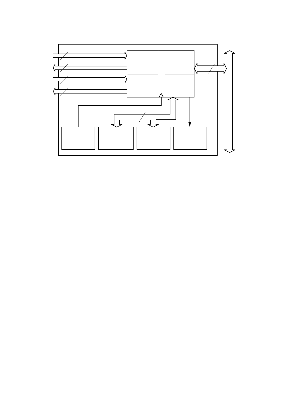
Figure 1.1 LSIFC929 Typical Implementation
2
FC
Channel 0
FC
Channel 1
2
2
2
Clock
(106 MHz)
(1 Mbyte typ.)
1.2.1 Multifunction PCI
Coupled with the dual channel operation, the LSIFC929 adds
multifunction capability on the PCI bus. This capability allows the host to
see two distinct “channels” or host adapters. Each channel provides full,
concurrent support for FCP Initiator, Target, and LAN protocols.
SSRAM
Integrated
Transceiver
Integrated
Transceiver
32
Flash
(1 Mbyte)
LSIFC929
Memory
Controller
EEPROM
(2 Kbyte)
PCI Bus
32/64
Serial
1.2.2 Simple Autospeed Negotiation Algorithm
Backward compatibility with 1 Gbit/s FC devices is maintained through
the use of the “Simple Autospeed Negotiation Algorithm.” After a
power-on, loss of signal, or loss of word synchronization for longer than
the R_T_TOV time-out, the LSIFC929 will perform this operation to
determine whether a point-to-point device or all of the devices on a loop
are either 1 Gbit/s or 2 Gbits/s devices.
1.2.3 Failover
The LSIFC929 supports two PCI functions and FC ports, which improves
performance and provides a redundant path in high-availability systems
that require failover capabilities. In case of a Link Failure, the LSIFC929
architecture allows the OS driver to support automatic failover, without
the need for IOC intervention.
General Description 1-5
Copyright © 2000, 2001 by LSI Logic Corporation. All rights reserved.
Page 20

1.3 Hardware Overview
In today’s fast growing server, RAID, and workstation marketplaces,
higher levels of performance, scalability and reliability are required to stay
competitive in the SAN market.
The LSIFC929 provides the performance and flexibility to meet
tomorrow’s FC connectivity requirements.
The LSIFC929 and the LSI Logic software drivers provide superior
performance and lower host CPU overhead than other competitive
solutions. Because of its high level of integration and streamlined
architecture, the LSIFC929 provides the highest level of performance in
a more cost effective FC solution.
Figure 1.2 shows the functional block diagram for the LSIFC929. The
architecture maximizes performance and flexibility by deploying fixed
gates in critical performance areas and utilizing multiple ARM RISC
processors (two for context management and an additional one for the
I/O Processor). Each of the major blocks is briefly described below.
1-6 Introduction
Copyright © 2000, 2001 by LSI Logic Corporation. All rights reserved.
Page 21
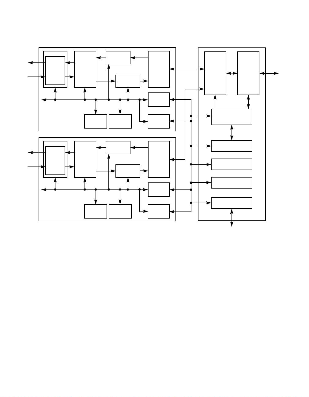
Figure 1.2 LSIFC929 Block Diagram
Tx
Rx
Channel [0]
Tx
Rx
SerDes
Giga
®
Blaze
Channel [0] ZBus
SerDes
Giga
Blaze
Channel [1] ZBus
Channel [1]
Link
Control
Link
Control
CtxMgr
CtxMgr
Transmitter
Receiver
ZArbiter
Transmitter
Receiver
ZArbiter
Channel
Arbiter/
Mux
Zbridge
ZQman
Channel
Arbiter/
Mux
Zbridge
ZQman
DMA[0]
DMA[1]
PCI
Arbitrator
System
Interface
IOP
ZArbiter
TimerCfg
XMem
PBSRAM
PCI
Interface
PCI
1.3.1 PCI Interface
The LSIFC929 uses a 64-bit (33 MHz or 64 MHz) PCI interface or a
32-bit (33 MHz or 64 MHz) PCI interface. In addition, support is provided
for Dual Address Cycle (DAC), PCI power management, Subsystem
Vendor ID and Vendor Product Data (VPD). Extended access cycles
(MRL, MRM, MWI) are also supported.
1.3.2 32-Bit Memory Controller
The memory controller provides access to Flash ROM and 32-bit
Synchronous SRAM. It supports both interleaved and noninterleaved
configurations up to a maximum of 4 Mbytes of synchronous SRAM. A
Hardware Overview 1-7
Copyright © 2000, 2001 by LSI Logic Corporation. All rights reserved.
Page 22

general purpose memory expansion bus supports up to 1 Mbyte of Flash
ROM.
1.3.3 I/O Processor
The LSIFC929 uses a 32-bit ARM RISC processor to control all system
interface and message transport functionality. This frees the host CPU
for other processing activity and improves overall I/O performance. The
RISC processor and associated firmware have the ability to manage an
I/O from start to finish without host intervention. The RISC processor also
manages the message passing interface.
1.3.4 System Interface
The system interface efficiently passes messages between the
LSIFC929 and other I/O agents. It consists of four hardware FIFOs for
the message queuing lists: Request Free, Request Post, Reply Free, and
Reply Post. Control logic for the FIFOs is provided within the LSIFC929
system interface with messages stored in external memory.
1.3.5 Integrated 2 Gbaud Transceivers
The LSIFC929 implements LSI Logic’s GigaBlaze®2 Gbaud integrated
transceivers. GigaBlaze is backward compatible with 1Gbaud systems,
using a firmware-implemented “Simple Autospeed Negotiation Algorithm”
for easy updates. The integrated 2 Gbaud transceivers provide a FC
compliant physical interface for cost conscious and real estate limited
applications.
1.3.6 Link Controllers
The integrated link controller is FC-AL-2 (Rev. 7.0) compatible and
performs all link operations. The controller monitors the Link State and
strictly adheres to the Loop Port State Machine ensuring maximum
system interoperability. The link control interfaces to the integrated
transceiver.
1-8 Introduction
Copyright © 2000, 2001 by LSI Logic Corporation. All rights reserved.
Page 23

1.3.7 Transmitters
The transmitter builds sequences based on context information and
transmits resulting frames to the FC link using the Link Controller. Each
transmitter includes two 2 Kbyte buffers to support frame payloads.
1.3.8 Receivers
The receivers accept frame data from the Link Controller and DMAs the
encapsulated information to local or system memory. Each receiver
contains three 2 Kbyte buffers which support a BB-Credit of up to three
or an Alternate Login BB-Credit of 1 on each channel.
1.3.9 Context Managers
The LSIFC929 uses an ARM RISC processor in each channel to support
I/O context swap to external memory and FCP management for both
Initiator and Target applications. Context operations include support for
transmit and resource queue management as well as scatter/gather list
management.
1.4 Initiator Operations
The LSIFC929 autonomously handles FCP exchanges upon request
from the host. The LSIFC929 generates appropriate sequences and
frames necessary to complete the request and provides feedback to the
host on the status of the request.
1.5 Target Operations
The LSIFC929 provides for general purpose target functions such as
those required for front-end RAID applications.
1.6 Diagnostics
The LSIFC929 provides the capabilities to do a simplified “Link Check”
Bit Error Rate (BER) test on the link for diagnostic purposes. In a special
test mode the controller can transmit and verify a programmed data
pattern for link evaluation.
Initiator Operations 1-9
Copyright © 2000, 2001 by LSI Logic Corporation. All rights reserved.
Page 24

1-10 Introduction
Copyright © 2000, 2001 by LSI Logic Corporation. All rights reserved.
Page 25

Chapter 2
Fibre Channel
Overview
This chapter provides general overview information on Fibre Channel
(FC). The chapter contains the following sections:
• Section 2.1, “Introduction”
• Section 2.2, “FC Layers”
• Section 2.3, “Frames”
• Section 2.4, “Exchanges”
• Section 2.5, “FC Ports”
• Section 2.6, “FC Topologies”
• Section 2.7, “Classes of Service”
2.1 Introduction
FC is a high-performance, hybrid interface. It is both a channel and a
network interface that contains network features to provide the required
connectivity, distance, protocol multiplexing, as well as traditional channel
features to retain the required simplicity, repeatable performance, and
guaranteed delivery. Popular industry standard networking protocols
such as Internet Protocol (IP) and channel protocols such as Small
Computer System Interface (SCSI) have been mapped to the FC
standard.
The FC structure is defined by five functional layers. These layers,
shown in Figure 2.1, define the physical media and transmission rates,
encoding scheme, framing protocol and flow control, common services,
and the Upper Level Protocol (ULP) interfaces.
LSIFC929 Dual Channel Fibre Channel I/O Processor 2-1
Copyright © 2000, 2001 by LSI Logic Corporation. All rights reserved.
Page 26
Figure 2.1 FC Layers
Behaviors
System
Interface
Logical
Layers
FC-4
Upper Layer Protocol (ULP)
IPESCONHIPPIIPI-3FCP
2.2 FC Layers
Common Services - e.g.,...Striping (not defined)
Framing Protocol/Flow Control
8b/10b Encode/Decode
8496424821241062
Mbits/s (Full Duplex) FC-PH-2
100 200 400 800
Physical
Layers
MBytes/s
FC-3
FC-2
FC-1
FC-0
The lowest layer, FC-0, is the media interface layer. It defines the
physical characteristics of the interface. It includes transceivers,
copper-to-optical transducers, connectors, and any other associated
circuitry necessary to transmit or receive at 1062 or greater Mbaud/s
rates over copper or optical cable.
The FC-1 layer defines the 8b/10b encoding/decoding scheme, the
transmission protocol necessary to integrate the data and transmit clock,
and the receive clock recovery. Implementation of this layer is usually
divided between the hardware implementing the FC-0 layer in a
transceiver, and the protocol device which implements the FC-2 layer.
Specifically, the FC-0 transceivers can include the clock recovery circuitry
while the 8b/10b encoding/decoding is provided in the protocol device.
The FC-2 layer defines the rules for the signaling protocol and describes
transfer of the Frames, Sequences, and Exchanges. The meaning of the
data being transmitted or received is transparent to the FC-2 layer.
However, the context between any given set of frames is maintained at
2-2 Fibre Channel Overview
Copyright © 2000, 2001 by LSI Logic Corporation. All rights reserved.
Page 27

2.3 Frames
the FC-2 layer through the Sequence and Exchange constructs. The
framing protocol creates the constructs necessary to form frames with
the data being packetized within each frame’s payload.
The FC-3 layer provides common services that span multiple N_Ports
(see Section 2.5, “FC Ports,” page 2-7). Some of these services include
Striping, Hunt Groups, and Multicasting. All of these services allow a
single port or fabric to communicate to several N_Ports at one time.
The top layer defined in FC is the FC-4 layer. The FC-4 layer provides a
seamless integration of existing standards. It specifies the mapping of
Upper Layer Protocols (ULPs) to the layers below. Some of these ULPs
include SCSI and IP. Each of these ULPs is defined in its own ANSI
document.
There are two types of frames used in FC: Link Control frames and Data
frames. Link Control frames contain no payload and are flow control
responses to Data frames. An example of a Link Control frame is the
ACK frame.
Figure 2.2 Link Control Frame
Start
of
Frame
(4)
( ) = Number of Bytes
Frame
Header
(24)
CRC
(4)
End
of
Frame
(4)
A Data frame is any frame which contains data in the payload field. An
example of a Data frame is the LOGIN frame.
Frames 2-3
Copyright © 2000, 2001 by LSI Logic Corporation. All rights reserved.
Page 28

Figure 2.3 Data Frame
( ) = Number of Bytes
In FC, an Ordered Set is a group of four 10-bit characters that provide
low level Link functions, such as frame demarcation and signaling
between two ends of a Link. All frames start with a Start-of-Frame (SOF)
and end with an End-of-Frame (EOF) Ordered Set. Each frame contains
at least a 24-byte header defining such things as Destination and Source
ID, Class of Service and type of frame (e.g., FCP or FC-LE). The biggest
field within a frame can be the payload field. If the frame is a Link Control
frame, then there is no payload. If it is a Data frame, then the frame will
contain a Payload field of up to 2112 bytes. Finally, the frame includes a
Cyclic Redundancy Check (CRC) field used for detection of transmission
errors, followed by the EOF Ordered Set.
2.4 Exchanges
Figure 2.4 outlines the FC hierarchical Data structures. At the most
elemental level, four 8b/10b encoded characters make up a FC Word. A
FC Frame is a collection of FC words. A FC Sequence is made up of
one or more frames, and a FC Exchange is made up of one or more
sequences.
Start
of
Frame
(4)
Frame
Header
(24)
Data Field
(Optional Headers and
Payload)
(0 to 2112)
CRC
(4)
End
of
Frame
(4)
2-4 Fibre Channel Overview
Copyright © 2000, 2001 by LSI Logic Corporation. All rights reserved.
Page 29
Figure 2.4 Exchange to Character
EXCHANGE
SEQ 1 SEQ 2 SEQ 4 SEQ N
FRAME 1 FRAME 2 FRAME 4 FRAME N
SOF HEADER DATA CRC EOF Frame
K28.5 D21.5 D23.0 WordD23.0
0 Character0 1 1 1 1 1 0 1 0
SEQ 3
FRAME 3
The following discussion illustrates an Exchange by considering a typical
parallel SCSI I/O. In parallel SCSI, there are several phases which make
up the I/O. These phases include Command, Data, Message, and Status
phases.
Using the FCP for the SCSI ULP, these phases can be mapped into the
other lower FC layers. Figure 2.5 shows the components that make up
the FCP exchange.
Exchanges 2-5
Copyright © 2000, 2001 by LSI Logic Corporation. All rights reserved.
Page 30
Figure 2.5 FCP Exchange
FCP EXCHANGE
CMDSEQ DataReqSEQ
FRAME 1
FRAME 1 FRAME 1
FRAME 2 FRAMEnFRAME 1
ResponseSEQDataSEQ
Figure 2.6 shows how the Exchange flows between the Initiator and
Target. The Initiator starts the FCP exchange by sending a Command
Sequence containing one frame to the Target. The Frame’s payload
contains the Command Descriptor Block (CDB). The Target will then
respond with a Data Delivery Request Sequence containing one Frame.
The payload of this Frame contains a XFER_RDY response. Once the
Initiator receives the Target’s response, it will begin sending the Data
Sequence(s), which may contain one or more Frames. This is analogous
to parallel SCSI’s DATA_OUT phase. When the Target has received the
last Frame of the Data Sequence(s), it will send a Response Sequence
containing one Frame to the Initiator, thus concluding the FCP Exchange.
2-6 Fibre Channel Overview
Copyright © 2000, 2001 by LSI Logic Corporation. All rights reserved.
Page 31

Figure 2.6 Write Event Trellis
2.5 FC Ports
Initiator
Fabric
CMD SEQ
Data SEQ Frame 1
Data SEQ Frame 2
Data SEQ Frame N
Target
Data Req SEQ
RSP SEQ
FC devices are called nodes. Each node has at least one port to provide
access to other ports in other nodes. The “port” is the hardware entity
within a node that performs data communications over the FC Link.
A variety of types of ports are defined within the FC standard, based on
the location of the port and the topology associated with it. The most
commonly used ports are N_Ports, NL_Ports, F_Ports, and FL_Ports.
These types of ports appear in Figure 2.7, Figure 2.8, and Figure 2.9.
2.6 FC Topologies
Topologies are defined, based on the capability and the presence or
absence of Fabric between the N_Ports:
• Point-to-Point topology
• Fabric topology
• Arbitrated Loop topology
FC-PH protocols are topology independent. Attributes of a Fabric may
restrict operation to certain communication models.
FC Ports 2-7
Copyright © 2000, 2001 by LSI Logic Corporation. All rights reserved.
Page 32

2.6.1 Point-to-Point Topology
The topology shown in Figure 2.7, in which communication between
N_Ports occurs without the use of Fabric, is defined as point-to-point.
Figure 2.7 Point-to-Point Topology
2.6.2 Fabric Topology
Figure 2.8 illustrates multiple N_Ports interconnected by a Fabric. This
topology uses the Destination_Identifier (D_ID) embedded in the Frame
Header to route the Frame through a Fabric to the desired Destination
N_Port.
Figure 2.8 Fabric Topology
N_Port
N_Port BN_Port A
F_Port
2.6.3 Arbitrated Loop Topology
The Arbitrated Loop topology permits 2 to 127 L_Ports to communicate
without the use of a Fabric, as in Fabric topology. The arbitrated loop
supports a maximum of one point-to-point circuit at a time. When two
L_Ports are communicating, the arbitrated loop topology supports
simultaneous, symmetrical bidirectional flow.
Figure 2.9 illustrates two independent arbitrated loop configurations,
each with multiple L_Ports attached. Each line in the figure between
L_Ports represents a single fibre. The lower configuration shows an
Arbitrated Loop composed of three NL_Ports and one FL_Port (a Public
Loop).
2-8 Fibre Channel Overview
Copyright © 2000, 2001 by LSI Logic Corporation. All rights reserved.
Fabric
F_Port
F_Port N_PortN_Port F_Port
N_Port
Page 33

Figure 2.9 Arbitrated Loop Topology
2.7 Classes of Service
NL_PortNL_Port
Private Loop
NL_PortNL_Port
Fabric
Element
FL_PortNL_Port
Public Loop
NL_PortNL_Port
There are several classes of service in FC. The different classes are
distinguished from each other in three ways: by the level of guarantee for
data being delivered, the order in which data is delivered, and how data
flow control is maintained.
Class 1 is a dedicated connection between two N_Ports. The data
delivered is guaranteed with a required acknowledgement frame (ACK),
which a Class 1 device uses for flow control. All frames are received in
order.
Class 2 is a connectionless class. The data delivered is guaranteed with
an ACK frame. The frames can be received out of order. Class 2 uses
both ACK frames and the R_RDY Ordered Set for flow control.
Class 3 is also a connectionless class (the data being delivered is not
guaranteed). The frames can be received out of order. Class 3 uses only
the R_RDY Ordered Set for flow control.
Classes of Service 2-9
Copyright © 2000, 2001 by LSI Logic Corporation. All rights reserved.
Page 34

Intermix is an enhancement of Class 1 service. A dedicated Class 1
connection may waste fabric bandwidth while frames are not being
transmitted or received between two N_Ports. In order to recover some
of this bandwidth, Intermix allows Class 2 and Class 3 frames to be
transmitted/received between Class 1 frames. N_Ports advertising
Intermix capability must be capable of receiving Class 2 and Class 3
frames from other N_Ports while maintaining the original Class 1 Link.
2-10 Fibre Channel Overview
Copyright © 2000, 2001 by LSI Logic Corporation. All rights reserved.
Page 35

Chapter 3
LSIFC929 Overview
This chapter provides a general description of the LSIFC929 Fibre
Channel PCI Protocol Controller firmware. The chapter contains the
following sections:
• Section 3.1, “Introduction”
• Section 3.2, “Message Interface”
• Section 3.3, “SCSI Message Class”
• Section 3.4, “LAN Message Class”
• Section 3.5, “Target Message Class”
• Section 3.6, “Support Components”
3.1 Introduction
The LSI Logic LSIFC929 is used to connect a host to a high speed FC
Link. The FCP ANSI standard, FC Private Loop Direct Attach, and Fabric
Loop Attach profiles are supported with the use of a sophisticated
firmware implementation. All profiles, specifications, and interoperability
maintained by the LSIFC929 are listed in Appendix B, “Reference
Specifications”.
Although optimized for a 64-bit PCI interface to communicate with the
system CPU(s) and memory, the LSIFC929 also supports a 32-bit PCI
environment. The system interface to the LSIFC929 is designed to
minimize the amount of PCI bandwidth required to support I/O requests.
A packetized message passing interface is used to reduce the number
of single cycle PCI bus cycles. All FC Data traffic on the PCI bus occurs
with zero wait state bursts across the PCI bus.
The intelligent LSIFC929 architecture allows the system to specify I/Os
at the command level. The LSIFC929 manages I/Os at the Frame,
LSIFC929 Dual Channel Fibre Channel I/O Processor 3-1
Copyright © 2000, 2001 by LSI Logic Corporation. All rights reserved.
Page 36

Sequence and Exchange level. Error detection and I/O retries are also
handled by the LSIFC929, allowing the system to offload part of the
exception handling work from the system driver.
3.1.1 Data Flows
The LSIFC929 uses a 64-bit (33 MHz or 66 MHz) PCI interface to pass
control and data information between the system and the protocol
controller. This interface is managed by the PCI Interface block, as
shown in Figure 3.1. It is backward compatible with 32-bit/33 or 66 MHz
buses.
Figure 3.1 LSIFC929 Block Diagram
Tx
Rx
Channel [0]
Tx
Rx
SerDes
Giga
Blaze
Channel [0] ZBus
SerDes
Giga
Blaze
Channel [1] ZBus
Channel [1]
Link
Control
Link
Control
CtxMgr
CtxMgr
Transmitter
Receiver
ZArbiter
Transmitter
Receiver
ZArbiter
Channel
Arbiter/
Mux
Zbridge
ZQman
Channel
Arbiter/
Mux
Zbridge
ZQman
DMA[0]
DMA[1]
PCI
Arbitrator
System
Interface
IOP
ZArbiter
TimerCfg
XMem
PBSRAM
PCI
Interface
PCI
For incoming serial data, the physical Link transfers the data to Link
Control using the GigaBlaze Integrated Transceiver. The Link Controller
analyzes the received frame and if appropriate, it passes the frame to the
3-2 LSIFC929 Overview
Copyright © 2000, 2001 by LSI Logic Corporation. All rights reserved.
Page 37

Receiver. The Receiver strips off the frame header and places it in a
separate header buffer while the data in the frame payload is placed in
a data buffer. The Frame Receiver uses the Receive Context Manager to
manage the received frame’s order and priority. The data contained in the
Receiver buffers is associated with a specific scatter/gather entry and
passed on to the PCI Interface and it requests the PCI bus and bursts
the data into system memory.
The I/O Processor, with its firmware, provides the translation from FC
specific protocols to the high level Block Storage, SCSI and LAN
message interface. This translation allows the LSIFC929 to be integrated
into the system as if it were a native Parallel SCSI or LAN device, hiding
all FC unique characteristics. Internal communication between the I/O
Processor and the Context manager occurs over an internal bus, which
is also connected to an External Memory Controller. The I/O Processor
uses the External Memory Controller to access local memory. This
memory contains the firmware, as well as the dynamic data structures
used by the firmware.
3.2 Message Interface
The LSIFC929 system interface is a high-performance, packetized,
mailbox architecture that leverages the intelligence in the LSIFC929 to
minimize traffic on the PCI bus.
3.2.1 Messages
There are two basic constructs in the Message Interface. The first
construct, the Message, is used to communicate between the system
and the LSIFC929. Messages are moved between the system(s) and the
LSIFC929 using the second construct, a Transport mechanism.
The LSIFC929 uses two types of messages to communicate with the
system. Request messages are created by the system to “request” an
action by the LSIFC929. Reply messages are used by the LSIFC929 to
send status information back to the system. Request message data
structures are up to 128 bytes in length. The message includes a
message header and a payload. The header includes information to
uniquely identify the message. The payload is specific to the Request
itself, and is unique for SCSI, LAN, and Target messages. For more
Message Interface 3-3
Copyright © 2000, 2001 by LSI Logic Corporation. All rights reserved.
Page 38

information regarding the details of the message format, refer to the
LSI Logic Fusion-MPT specification.
3.2.2 Message Flow
Before Requests can be posted to the LSIFC929, the system must
allocate and initialize a pool of message frames, and provide a
mechanism to assign individual message frames, on a per-request basis.
The host must also provide one message frame per target LUN, and
prime the Reply Free FIFOs for each function with the physical address
of these message frames. Once allocation has been completed, requests
will flow from the host to the LSIFC929, as represented below and in
Figure 3.2.
1. The host driver receives an I/O request from the operating system.
2. The host driver allocates a system message frame and builds an I/O
request message within the SMF. The allocation method is the
responsibility of the host driver.
3. The host driver creates the Message Frame Descriptor (MFD), and
writes the MFD to the Request Post FIFO.
4. The IOC reads the MFD from the Request Post FIFO and DMA’s the
request to a local message frame.
5. The IOC sends the appropriate Fibre Channel request, and
subsequently receives the reply from the target.
– If the I/O status was successful, the IOC writes the
MessageContext value, plus turbo reply bits, to the Reply Post
FIFO, which automatically generates a system interrupt.
– If the I/O status was not successful, the IOC pops a reply
message frame from the Reply Free FIFO, and generates a reply
message in the reply message frame. The IOC then writes the
system physical address of the reply message frame to the
Reply Post FIFO, which generates a system interrupt.
6. The host driver receives an interrupt and reads the Reply Register.
If there are no posted messages, the system reads the value
0xFFFFFFFF.
7. The host driver responds to the Operating System appropriately.
8. If the I/O status was not successful, the host driver returns it to the
Reply Free FIFO.
3-4 LSIFC929 Overview
Copyright © 2000, 2001 by LSI Logic Corporation. All rights reserved.
Page 39

Figure 3.2 LSIFC929 Message Flow
Operating System
71
1
2
3
Message
Frames
2
Host Driver
MFD
PCI Bus
Request
Post
FIFO
1
2
N
3
Request Register
3
Reply Register
IOC
3.3 SCSI Message Class
The SCSI message interface provides the most direct interface for
block-oriented storage media. This includes disk drives and tape devices.
The SCSI I/O path translates a SCSI CDB into an FCP exchange. All FC
device and target discovery operations are managed completely within
the LSIFC929. FC target devices are assigned a logical (bus, target ID)
identifier, and are accessed by the system as if they were parallel SCSI
devices. The system is responsible for scanning the target devices, and
identifying LUNs on the target devices.
6
6
5
54
1
2
N
Reply
Post
FIFO
N
8
1
2
N
Reply
Free
FIFO
In general, the system is responsible for retrying operations at an I/O
request level. The LSIFC929 is responsible for responding to bus
SCSI Message Class 3-5
Copyright © 2000, 2001 by LSI Logic Corporation. All rights reserved.
Page 40

protocol-specific errors and exceptions and retrying bus sequences
within the scope of an I/O operation. The system is also responsible for
maintaining a timer for SCSI I/O operations if this is required by the host
system. The host driver may use the provided SCSI Task Management
functions to terminate one or more I/O operations when a timeout occurs.
For more information regarding the SCSI Message Class, refer to the
LSI Logic Fusion-MPT specification.
3.4 LAN Message Class
The LSIFC929 provides a LAN message interface that supports the
system TCP or UDP network driver stack, providing MAC level
communication between FC ports.
The typical network driver stack in the system consists of a Socket Driver
with a Transport Driver Interface, supported by TCP or UDP and IP
drivers, and a Hardware Abstraction layer interface to the LSIFC929. The
TCP driver provides data buffer segmentation. The IP driver provides
MTU segmentation, adds a header and checksum to the TCP data, and
maps each Fibre Channel MAC port address to an IEEE standard
address. ACKs are required at the TCP driver to ensure all segments of
the data block are transmitted/received.
The LAN message interface may also be used by proprietary protocol
stacks in the host, as shown in Figure 3.3. In this environment, the
LSIFC929 transmits and receives data between FC nodes, without
regard to data content. For more information regarding the LAN Message
Class, refer to the LSI Logic Fusion-MPT specification.
3-6 LSIFC929 Overview
Copyright © 2000, 2001 by LSI Logic Corporation. All rights reserved.
Page 41

Figure 3.3 LAN Protocol Stack
Applications
IEEE
Address
IP Header
w/Checksum
IP Header
w/Checksum
MAC Header FC Sequence/Frame
TCP Header
w/Checksum
TCP Header
w/Checksum
TCP Header
w/Checksum
16 Kbytes
Paged Data
TCP Data (var)
TCP Data (var)
TCP Data (var)
Sockets Interface
Transport
Driver Interface
Transmission
Control Protocol
Internet
Protocol Driver
Driver Interface
HAL
PCI
LSIFC929 LAN Class
FC Framer
FC
3.5 Target Message Class
The Target interface allows the LSIFC929 to be used as the system
interface for FC bridge controllers. The LSIFC929 provides an FCP
exchange level message interface that routes commands to the system.
The system identifies the appropriate data, and passes a Scatter Gather
List (SGL) to the LSIFC929 describing the data to transfer. A single
Target message directs the LSIFC929 to send a Xfer_Rdy, as needed,
and to transfer data and FCP response. Target specific Process
Login/Logout is managed by the system. For more information regarding
the Target Message Class, refer to the LSI Logic Fusion-MPT
specification.
Target Message Class 3-7
Copyright © 2000, 2001 by LSI Logic Corporation. All rights reserved.
Page 42

3.6 Support Components
The memory controller block within the LSIFC929 provides access to
external local memory resources required to manage FCP.
The following sections provide guidance in choosing the support
components necessary for a fully functional implementation using the
LSIFC929. A LSIFC929 typical implementation diagram is shown below
in Figure 3.4 for reference.
Figure 3.4 LSIFC929 Typical Implementation
2
FC
Channel 0
FC
Channel 1
2
2
2
Clock
(106 MHz)
(1 Mbyte typ.)
3.6.1 SSRAM Memory
The primary function of this memory is to store data structures used by
the LSIFC929 to manage exchanges and transmit and receive queues.
The SSRAM memory also stores part of the run time image of the
LSIFC929 firmware, such as initialization and error recovery code. The
mainline code is stored within the internal LRAM for performance
reasons.
SSRAM
Integrated
Transceiver
Integrated
Transceiver
32
Flash
(1 Mbyte)
LSIFC929
Memory
Controller
EEPROM
(2 Kbyte)
PCI Bus
32/64
Serial
The LSIFC929 uses a 32 bit nonmultiplexed memory bus to access the
SSRAM. This memory bus has the capability to address up to 4 Mbytes
of SSRAM.
3-8 LSIFC929 Overview
Copyright © 2000, 2001 by LSI Logic Corporation. All rights reserved.
Page 43

The LSIFC929 firmware also supports optional byte wide parity error
detection. This option is configurable, and is specified as a serial
EEPROM parameter.
The amount of SSRAM (1 Mbyte) determines the maximum number of
outstanding Request Messages (1024). This roughly equates to the
maximum number of outstanding I/O requests pending in the LSIFC929.
3.6.2 Flash ROM
The memory controller in the LSIFC929 also manages an optional Flash
ROM. If present, the Flash ROM is used to store the firmware for the
LSIFC929 I/O Processor, and if desired, the INT 0x13 boot software.
If the Flash ROM is not used, then the host platform is responsible for
downloading the I/O Processor firmware to the LSIFC929 through the
PCI interface. The LSIFC929 supports a diagnostic interface, enabled
through a sequence of commands issued to the PCI configuration space.
Firmware may be directly written to the LSIFC929 internal memory and
external SSRAM through the diagnostic interface. Details of this
implementation are available in the LSI Logic Fusion-MPT specification.
Flash ROM is optional for the LSIFC929, but it is required for firmware
storage if INT 0x13 boot software is used. Flash ROM also simplifies OS
driver requirements and implementations.
The Flash ROM is accessed using the upper eight bits of the Memory
Interface. If a Flash ROM is to be used, then it should have a capacity
of 1 Mbyte with a maximum access time of 150 ns. Please see the
LSI Logic Fusion-MPT specification for more information regarding the
programming of the Flash ROM.
3.6.3 Serial EEPROM
The serial EEPROM stores nonvolatile data for the LSIFC929, such as
the World Wide Name, VPD, and other vendor specific information. The
SEEPROM data is programmed by the firmware, so the firmware must
be downloaded and running before the SEEPROM is programmed. The
minimum required size of the EEPROM is 2 Kbytes; however, an 8 Kbyte
SEEPROM is required for full functionality.
Support Components 3-9
Copyright © 2000, 2001 by LSI Logic Corporation. All rights reserved.
Page 44

3-10 LSIFC929 Overview
Copyright © 2000, 2001 by LSI Logic Corporation. All rights reserved.
Page 45

Chapter 4
Signal Descriptions
This chapter contains signal descriptions for the LSIFC929. A slash (/)
indicates an active low signal, I/O = bidirectional signal, I = input signal,
O = output signal, T/S = 3-state, and S/T/S = sustained 3-state.
Figure 4.1 on page 4-2 is a functional signal grouping for the chip.
LSIFC929 Dual Channel Fibre Channel I/O Processor 4-1
Copyright © 2000, 2001 by LSI Logic Corporation. All rights reserved.
Page 46

Figure 4.1 LSIFC929 Functional Signal Grouping
LSIFC929
Memory
Interface
PCI
Interface
ZZ
FLASHCS/
RAMCS/
MA[21:0]
MD[31:0]
MP[3:0]
ADV/
ADSC/
BWE[3:0]/
MWE[1:0]/
MOE[1:0]/
MCLK
AD[63:0]
GNT/
C_BE[7:0]/
FRAME/
TRDY/
STOP/
SERR/
INTA/
INTB/
RST/
REQ/
IDSEL
IRDY/
DEVSEL/
PERR/
PAR
REQ64/
ACK64/
PAR64
PCICLK
ENUM/
64EN/
SWITCH
HOTSWAPEN/
TX0+
TX0−
TX1+
TX1−
RX0+
RX0−
RX1+
RX1−
RTRIM
LIPRESET/
FAULT0/
FAULT1/
ODIS0
ODIS1
BYPASS0/
BYPASS1/
RXLOS0
RXLOS1
MODDEF0[2:0]
MODDEF1[2:0]
REFCLK/
TCK
TRST/
TDI
TDO
TMS_CHIP
TMS_ICE
IDDTN
PROC_DRVLS
ARMEN/
TESTRESET/
MODE[7:0]
ROMSIZE[1:0]
FSELZ[1:0]
ZCLK
GPIO[3:0]
LED[4:0]/
SCL
SDA
Fibre Channel
Interface
JTAG and
Core Debug
Configuration
and
Miscellaneous
4-2 Signal Descriptions
Copyright © 2000, 2001 by LSI Logic Corporation. All rights reserved.
Page 47

Table 4.1 PCI Interface
Signal I/O
Number Pad Type Description
PCICLK I AA13 5 V Tol In Clock provides timing for all transactions on the
PCI bus and is an input to every PCI device. All
other PCI signals are sampled on the rising
edge of PCICLK, and other timing parameters
are defined with respect to this edge.
RST/ I T3 5 V Tol In Reset forces the PCI sequencer of the device
to a known state. All 3-state and sustained
3-state signals are forced to a high impedance
state, and all internal logic is reset. The RST/
input is synchronized internally to the rising
edge of PCICLK. The PCICLK input must be
active while RST/ is asserted to properly reset
the device.
BGA Pad
GNT/ I V1 5 V Tol
BiDir PCI
Grant indicates to the agent that access to the
PCI bus has been granted. This is a
point-to-point signal. Every master has its own
GNT/.
REQ/ O V2 5 V Tol
BiDir PCI
Request indicates to the system arbiter that
this agent desires use of the PCI bus. This is a
point-to-point signal. Every master has its own
REQ/.
REQ64/ O AA15 5 V Tol
BiDir PCI
Request64 indicates that the current bus
master desires to transfer data using 64 bits.
REQ64/ is sampled at the end of reset to
indicate the presence of a 64-bit bus.
ACK64/ S/T/S Y15 5 V Tol
BiDir PCI
Copyright © 2000, 2001 by LSI Logic Corporation. All rights reserved.
Acknowledge64 is an input from the Target
that decodes the address, and indicates that
the Target is willing to complete a 64-bit
transfer. No slaves on the LSIFC929 assert this
pin (i.e., all slaves are 32-bit slaves). The
LSIFC929 will not assert this pin when
accessed as a Target, but will monitor this pin
when initiating transfers (i.e., the LSIFC929
presents itself as a 32-bit slave device, but
operates as a 64-bit bus master).
4-3
Page 48

Table 4.1 PCI Interface (Cont.)
Signal I/O
Number Pad Type Description
AD[63:0] T/S AC18, AB18,
AA18, AC19
AB19, AA19,
AC20, AB20
AC21, AA20,
AC22, AB21
AC23, AB22,
AA22, AB23
AA23, Y22,
Y23, W21
W22, W23,
V21, V22
V23,U22,U23,
T21, T20, T22,
T23, R21
V3, W1, W2,
W3, Y1, Y2,
AA1, AB1
AB2, AB3,
AC2, AA4,
AC3, AB4,
AC4, AA5
AC8, AA9,
AB9, AC9,
AA10, Y11,
AB10, AC10,
AC11, AB11,
AC12, AB14,
Y13, AA14,
AC15, AB15
BGA Pad
5VTol
BiDir PCI
The physical longword Address and Data are
multiplexed on the same PCI pins. During the
first clock of a transaction, AD[63:0] contains a
physical byte address. During subsequent
clocks, AD[63:0] contains data. A bus
transaction consists of an address phase
followed by one or more data phases. PCI
supports both read and write bursts. AD[7:0]
define the least significant byte, and AD[63:56]
define the most significant byte.
C_BE[7:0]/ T/S AC16, AB16,
AC17, AB17,
5VTol
BiDir PCI
AA2, AB5,
AB8, AA11
IDSEL I AC1 5 V Tol
BiDir PCI
4-4 Signal Descriptions
Copyright © 2000, 2001 by LSI Logic Corporation. All rights reserved.
Bus Command and Byte Enables are
multiplexed on the same PCI pins. During the
address phase of a transaction, C_BE[3:0]/
define the bus command. During the data
phase, C_BE[7:0]/ are used as byte enables.
The byte enables determine which byte lanes
carry meaningful data. C_BE[0]/ applies to the
least significant byte, and C_BE[7]/ to the most
significant byte. Byte enables are active LOW.
Initialization Device Select is used as a chip
select in place of the upper 24 address lines
during configuration read and write
transactions.
Page 49

Table 4.1 PCI Interface (Cont.)
Signal I/O
Number Pad Type Description
FRAME/ S/T/S AC5 5 V Tol
BiDir PCI
IRDY/ S/T/S AA6 5 V Tol
BiDir PCI
TRDY/ S/T/S AB6 5 V Tol
BiDir PCI
BGA Pad
Cycle Frame is driven by the current master to
indicate the beginning and duration of an
access. FRAME/ is asserted to indicate a bus
transaction is beginning. While FRAME/ is
deasserted, the transaction is in the final data
phase or the bus is idle.
Initiator Ready indicates the initiating agent’s
(bus master’s) ability to complete the current
data phase of the transaction. IRDY/ is used
with TRDY/. A data phase is completed on any
clock when both IRDY/ and TRDY/ are sampled
asserted. During a write, IRDY/ indicates that
valid data is present on AD[63:0]. During a
read, it indicates that the master is prepared to
accept data. Wait cycles are inserted until both
IRDY/ and TRDY/ are asserted together.
Target Ready indicates the target agent’s
(selected device’s) ability to complete the
current data phase of the transaction. TRDY/ is
used with IRDY/. A data phase is completed on
any clock when used with IRDY/. A data phase
is completed on any clock when both TRDY/
and IRDY/ are sampled asserted. During a
read, TRDY/ indicates that valid data is present
on AD[63:0]. During a write, it indicates that the
target is prepared to accept data. Wait cycles
are inserted until both IRDY/ and TRDY/ are
asserted together.
DEVSEL/ S/T/S AC6 5 V Tol
BiDir PCI
STOP/ S/T/S AA7 5 V Tol
BiDir PCI
Copyright © 2000, 2001 by LSI Logic Corporation. All rights reserved.
Device Select indicates that the driving device
has decoded its address as the target of the
current access. As an input, it indicates to a
master whether any device on the bus has
been selected.
Stop indicates that the selected target is
requesting the master to stop the current
transaction.
4-5
Page 50

Table 4.1 PCI Interface (Cont.)
Signal I/O
Number Pad Type Description
PERR/ S/T/S AB7 5 V Tol
BiDir PCI
SERR/ O AC7 5 V Tol
BiDir PCI
PAR T/S AA8 5 V Tol
BiDir PCI
PAR64 T/S AA17 5 V Tol
BiDir PCI
INTA/ O U2 5 V Tol
BiDir PCI
BGA Pad
Parity Error may be pulsed active by an agent
that detects a parity error. PERR/ can be used
by any agent to signal data corruption.
However, on detection of a PERR/ pulse, the
central resource may generate a nonmaskable
interrupt to the host CPU, which often implies
the system will be unable to continue operation
once error processing is complete.
System Error is an open drain output used to
report address parity errors and data parity
errors on the Special Cycle command.
Parity is the even parity bit that protects the
AD[31:0] and C_BE[3:0]/ lines. During the
address phase, both the address and
command bits are covered. During the data
phase, both data and byte enables are covered.
Parity64 is the even parity bit that protects the
AD[63:32] and C_BE[7:4]/ lines. During the
address phase, both the address and
command bits are covered. During the data
phase, both data and byte enables are covered.
Interrupt A. This open-drain signal, when
asserted LOW, indicates that PCI Function[0] is
requesting service from its Host device driver.If
the chip is configured as a single-function
device, only INTA/ is used.
INTB/ O U1 5 V Tol
BiDir PCI
4-6 Signal Descriptions
Copyright © 2000, 2001 by LSI Logic Corporation. All rights reserved.
Interrupt B. This open-drain signal, when
asserted LOW, indicates that PCI Function[1] is
requesting service from its Host device driver.If
the chip is configured as a single-function
device, only INTA/ is used.
Page 51

Table 4.1 PCI Interface (Cont.)
Signal I/O
ENUM/ B AC13 5 V Tol
Number Pad Type Description
ENUM/. This signal must be asserted by a hot
BiDir PCI
swap capable card immediately after insertion
and during removal. This signal notifies the
system host either that a board has been
freshly inserted or that one is about to be
extracted, and informs the system host that the
configuration of the system has changed. The
system host then can perform any necessary
maintenance such as installing a device driver
upon board insertion, or quiescing a device
driver and the board, prior to the board’s
extraction.
BGA Pad
64EN/ B AC14 5 V Tol
BiDir PCI
PCI Bus Width Enable. This signal indicates
the width of the bus when hot swap capability
is enabled.
SWITCH I A1 5 V Tol In Insertion/Deassertion Indicator. This signal is
an input to the LSIFC929 to signal the insertion
or impending extraction of a board. This signal
causes the assertion of ENUM/. The operator
normally activates the switch (actuator), waits
for the illumination of the LED, and then
extracts the board.
HOTSWAPEN/
I M3 5 V Tol In Hot Swap Enable. When this signal is LOW,
the LSIFC929 is configured to comform to hot
swap protocol. This includes changing the bus
width detection method, the addition of
configuration registers, and support for the
ENUM/, BLUELED/ and SWITCH pins.
GPIO[2]
(BLUELED/)
B C5 3.3 V
BiDir
8mA
w/pullup
Copyright © 2000, 2001 by LSI Logic Corporation. All rights reserved.
GPIO[2] (BLUELED/). This signal will drive a
blue LED that is mounted on the front of hot
swap capable host adapters. This signal
indicates that the system software has been
placed in a state for orderly extraction of the
board. See also the description of the GPIO[2]
pin in Table 4.5, page 4-14, for additional
information regarding other operational
capabilities of this signal.
4-7
Page 52

Table 4.2 Fibre Channel Interface
Signal I/O
Number Pad Type Description
TX0+ O N2 Diff Tx Transmit differential data (Channel0).
TX1+ O H2 Diff Tx Transmit differential data (Channel1).
BGA Pad
TX0
− O N1 Diff Tx Transmit differential data (Channel0).
TX1
− O H1 Diff Tx Transmit differential data (Channel1).
RX0+ I L2 Diff Rx Receive differential data (Channel0).
RX1+ I G1 Diff Rx Receive differential data (Channel1).
RX0
− I L1 Diff Rx Receive differential data (Channel0).
RX1
− I G2 Diff Rx Receive differential data (Channel1).
RTRIM I L4 This pin is the analog current reference for the
integrated transceiver core. A 2.74 kΩ±1%
resistor should be tied from the RTRIM pad to
either the RXVDD0 or the RXVDD1 pin.
LIPRESET/ O R1 3.3 V BiDir
4mA
This pin is asserted LOW when a selective
reset is received that is targeted to one of this
device’s aliases. This pin is asserted for 1–2 ms
after the last LIPr is received.
FAULT0/ I R2 3.3 V TTL
Input
w/pullup
This active-LOW pin indicates that an electrical
fault has been detected by the channel0 PHY
device/module and, if the module has a laser,
the laser has been turned off. This pin causes
no interrupt or other reaction. It is assumed that
a Link Failure will occur and the register bit
reporting this pin’s value will be used to
diagnose the problem.
FAULT1/ I F3 3.3 V TTL
Input
w/pullup
ODIS0 O R3 3.3 V BiDir
4mA
4-8 Signal Descriptions
Copyright © 2000, 2001 by LSI Logic Corporation. All rights reserved.
This active-LOW pin indicates that an electrical
fault has been detected by the the channel1
PHY device/module and, if the module has a
laser, the laser has been turned off. This pin
causes no interrupt or other reaction. It is
assumed that a Link Failure will occur and the
register bit reporting this pin’s value will be
used to diagnose the problem.
Output Disable, Channel0. This output when
asserted disables an external GBIC or MIA
transmitter for channel0. This output is also
used to clear a module fault.
Page 53

Table 4.2 Fibre Channel Interface
Signal I/O
Number Pad Type Description
ODIS1 O J1 3.3 V BiDir
4mA
BYPASS0/ O T1 3.3 V BiDir
4mA
BYPASS1/ O K3 3.3 V BiDir
4mA
RXLOS0 I P3 3.3 V 4 mA
BiDir
w/pulldown
BGA Pad
Output Disable, Channel1. This output when
asserted disables an external GBIC or MIA
transmitter for channel1. This output is also
used to clear a module fault.
This line is driven LOW when the LSIFC929
Link Controller block has determined that
channel0 of the device is operating in a loop
environment and the device has entered a
bypassed mode. This may be caused by an
internal request or a loop primitive generated
by another node.
This line is driven LOW when the LSIFC929
Link Controller block has determined that
channel1 of the device is operating in a loop
environment and the device has entered a
bypassed mode. This may be caused by an
internal request or a loop primitive generated
by another node.
This line is driven HIGH, disabling the on-chip
receiver, when the GBIC for channel0 of the
LSIFC929 has detected a loss of signal. If
enabled through the Link Control Register, this
signal becomes an output test strobe.
RXLOS1 I E1 3.3 V 4 mA
BiDir
w/pulldown
MODDEF0[2:0] I A9, C10,
D11
3.3 V BiDir
8mA
w/pullup
MODDEF1[2:0] I B10, A10,
C11
3.3 V BiDir
8mA
w/pullup
REFCLK I E2 3.3 V
Schmitt
Input
Copyright © 2000, 2001 by LSI Logic Corporation. All rights reserved.
This line is driven HIGH, disabling the on-chip
receiver, when the GBIC for channel1 of the
LSIFC929 has detected a loss of signal. If
enabled through the Link Control Register, this
signal becomes an output test strobe.
GBIC and pluggable SFF optical module
Identifiers (channel0).
GBIC and pluggable SFF optical module
Identifiers (channel1).
FC reference clock (106.25 MHz ± 100 ppm).
4-9
Page 54

Table 4.3 Memory Interface
Signal I/O
MD[31:0]
I/O H22,H20, H21,
MD[31:24]
Number Pad Type Description
G23,G22,G21,
F23, F22, E21,
E23, E22, F21
D23, D22, C23,
D21, B18, A18,
C17, B17, A17,
C16, B16, A16
C15, B15, A15,
C14, D13, B14,
A14, C13
MP[3:0] I/O H23,B23, D18,
A13
MA[21:0] R20, P21, R23,
R22, N20, P23,
P22, N21, N23,
N22, M23, M21
M22, L22, L21,
L23, K23, K22,
J23, K21, J22,
J21
BGA Pad
3.3 V
BiDir
4mA
3.3 V
4mA
BiDir
w/pullup
3.3 V
BiDir
4mA
SSRAM Read/Write Data.
MD[31:24] are used for the FLASH ROM
Read/Write Data.
Memory Parity. Byte lane parity as follows:
MP [0]: Parity for MD[7: 0]
MP [1]: Parity for MD[15: 8]
MP [2]: Parity for MD[23:16]
MP [3]: Parity for MD[31:24]
Memory Parity may be optionally even, odd, or
none (not used) as defined in the LSIFC929
Programming Model.
SSRAM/FLASH ROM Address.
MOE[1:0]/ O B19, A19 3.3 V
BiDir
8mA
MWE[1:0]/ O B20, A20 3.3 V
BiDir
4mA
FLASHCS/ O C18 3.3 V
BiDir
4mA
4-10 Signal Descriptions
Copyright © 2000, 2001 by LSI Logic Corporation. All rights reserved.
Memory Output Enable. When asserted LOW,
the selected SRAM or FLASH (MOE[1]/) device
may drive data. This signal is typically an
asynchronous input to SRAM and/or FLASH
devices. The two output enables allow for
interleaving configurations, with MOE[0]/ being
the only output enable used for a
noninterleaved implementation.
Memory Write Enables. These active LOW
bank write enables are required for interleaving
configurations. MWE[0]/ is the only write enable
used for a noninterleaved implementation.
FLASH Chip Select. This active-LOW chip
select allows connection of a single 8-bit
FLASH ROM device.
Page 55

Table 4.3 Memory Interface (Cont.)
Signal I/O
Number Pad Type Description
MCLK O A23 3.3 V
8 mA T/S
Output
ADSC/ O C22 3.3 V
4 mA T/S
Output
ADV/ O B22 3.3 V
4 mA T/S
Output
BGA Pad
BWE[3:0]/ O B21, A22, C20,
A21
3.3 V
BiDir
4mA
RAMCS/ O C19 3.3 V
BiDir
4mA
ZZ O D19 3.3 V
BiDir
4mA
Memory Clock. All synchronous RAM
control/data signals are referenced to the rising
edge of this clock. Exceptions are MOE/ and
ZZ which are typically asynchronous inputs to
SRAM and/or FLASH devices.
Address-Strobe-Controller. Initiates READ,
WRITE, or chip deselect cycle. When this
signal is asserted, it also latches the memory
address signals.
Advance. When asserted LOW, the ADV/ input
causes a selected synchronous SRAM to
increment its burst address counter.
Memory Byte Write Enables. These
active-LOW, byte lane write enables allow
writing of partial words to memory.
RAM Chip Select. This pin is an active-LOW
synchronous chip select for all SSRAMS (up to
four SSRAMS for interleaved and depth
expanded configuration without additional
decode logic).
Snooze Control. Asserting this output HIGH
will cause a synchronous SRAM to enter its
lowest power state (not all RAMs support this
function).
Copyright © 2000, 2001 by LSI Logic Corporation. All rights reserved.
4-11
Page 56

Table 4.4 Configuration Signals
Signal I/O
ROMSIZE
[1:0]
Number Pad Type Description
I C12, A12 3.3 V TTL
Input
w/pullup
TESTRESET/ I A11 3.3 V
Schmitt
Input
w/pullup
ARMEN/ I B13 3.3 VTTL
Input
w/pullup
FSELZ[1:0] I A3, B4 3.3VTTL
Input
w/pullup
BGA Pad
This field identifies the size of the ROM that is
connected to the device. The value of this bus should
be established at chip reset and should remain
unchanged until another chip reset. The encoding of
this field is as follows:
Bits [1:0] ROM Size
00 256 Kbytes
01 512 Kbytes
10 1024 Kbytes
11 No external memory present
Test Reset. This pin forces the chip into the
Power-On-Reset state or Soft-Reset state, depending
on the state of the Mode pins.
When this pin is asserted LOW, the ARM RISC
processor core (IOP) is enabled and will boot from
FLASH ROM following chip reset. If this configuration
pin is held high, the IOP core will be held reset until
the DisARM bit in the Diagnostic register is cleared
by the Host CPU.
Frequency Select. These pins indicate how the
RefClk input (106.25 MHz) is internally divided to
generate the internal ZClk source. When FSELZ[1] is
HIGH, the internal ZClk tree is sourced directly from
the ZCLK input signal.
FSELZ[1:0] Internal ZClk
00 REFCLK/2
01 REFCLK * 2/3
10 External ZCLK
11 External ZCLK
4-12 Signal Descriptions
Copyright © 2000, 2001 by LSI Logic Corporation. All rights reserved.
Page 57

Table 4.4 Configuration Signals (Cont.)
Signal I/O
Number Pad Type Description
MODE[7:0] I A5, C6, D6,
B6, A6, C7,
B7, A7
BGA Pad
3.3VTTL
Input
w/pullup
Mode Select. This 8-bit bus defines operational and
test modes for the chip. Valid Mode encodings are
given below.
Mode[7:0] = 001xxxxx == Interleaved BSRAM
Mode[7:0] = 000xxxxx == Noninterleaved BSRAM
Mode[7:0] = 00xx1xxx == Link Reset Mode
Mode[7:0] = 00xxx1xx == Soft Reset Mode
Mode[7:0] = 00xxxx11 == Normal SEPROM Autoload
Mode[7:0] = 00xxxx10 == Fast SEPROM Autoload
Mode[7:0] = 00xxxx01 == Firmware PCI Config Mode
(ARMEN/ must also be low)
Mode[7:0] = 00xxxx00 == PCI Config use default
values
Copyright © 2000, 2001 by LSI Logic Corporation. All rights reserved.
4-13
Page 58

Table 4.5 Miscellaneous Signals
Signal I/O
Number Pad Type Description
GPIO[3:0] I/O A4, C5, D5, B5 3.3 V
BiDir
8mA
w/pullup
LED[4:0]/ O C8, B8, A8, C9,B93.3 V
BiDir
8mA
SCL O B11 3.3 V
4mA
BiDir
w/pullup
BGA Pad
General Purpose I/O Pins. These pins default
to input mode on reset. These signals are
controlled/observed by firmware and may be
configured as inputs or outputs. GPIO[3] may
be optionally enabled as an external interrupt
source to the ARM RISC Processor core. See
also the description of the GPIO[2] pin in
Table 4.1, page 4-7, for additional information
regarding other operational capabilities of this
signal.
These output signals may be controlled by
firmware or driven by chip activity. When
configured as activity driven, the LED[n]
outputs have the following meaning when
asserted LOW:
LED[4]: Channel 1 – Fault
LED[3]: Channel 1 – Active
LED[2]: Channel 0 – Fault
LED[1]: Channel 0 – Active
LED[0]: Firmware controlled (Heartbeat)
Serial EEPROM clock.
SDA I/O B12 3.3 V
4mA
BiDir
w/pullup
ZCLK I B3 3.3 V
Schmitt
Input
4-14 Signal Descriptions
Copyright © 2000, 2001 by LSI Logic Corporation. All rights reserved.
Serial EEPROM data.
External ZBus reference clock. Based on the
table below, this input pin provides the
reference timing for the internal ZBus, IOP and
CtxMgr processors, and memory interface.
When FSELZ[1] is high, the internal ZClk tree
is sourced directly from the ZCLK input signal.
FSELZ[1:0] Internal ZClk
00 REFCLK/2
01 REFCLK * 2/3
10 External ZCLK
11 External ZCLK
Page 59

Table 4.6 JTAG Test and I/O Processor Debug
Signal I/O
Number Pad Type Description
TCK I D3 3.3 V
Schmitt
w/pullup
TRST/ I C1 3.3 V
Schmitt
w/pullup
TDI I D1 3.3 V
Schmitt
w/pullup
TDO O E3 3.3 V
4 mA T/S
Output
w/pullup
TMS_CHIP I B1 3.3 V
Schmitt
w/pullup
TMS_ICE I D2 3.3 V
Schmitt
w/pullup
IDDTN I B2 Input
w/”large”
pulldown
BGA Pad
JTAG/CtxMgr Debug Test Clock.
JTAG/Debug Test Reset. Asynchronous
active-LOW.
JTAG/CtxMgr Debug Test Data In.
JTAG/CtxMgr Debug Test Data Out.
JTAG Test Mode Select.
CtxMgr Debug Test Mode Select.
QIDD Test Enable.
PROC_DRVLS O C2 Process Monitor Test Output Driver.
Copyright © 2000, 2001 by LSI Logic Corporation. All rights reserved.
4-15
Page 60

Table 4.7 Power and Ground Pins
Signal BGA Pad Number Description Voltage
VDDIO D10, D14, D17, D7
I/O power. 3.3 V
G20, G4, K20, K4
P20, P4, U20, U4
Y10, Y14, Y17, Y7
VSSIO AA21, AA3, C21, C3
I/O ground. 0 V
D12, D20, D4, K10
K11, K12, K13, K14
L10, L11, L12, L13
L14, M10, M11, M12
M13, M14, M20, M4
N10, N11, N12, N13
N14, P10, P11, P12
P13, P14, Y12, Y20, Y4
VDDC D9, D15, F20, F4, L20
Core power. 2.5 V
N4, V20, V4, Y16, Y8
VSSC D16, D8, E20, E4, J20
Core ground. 0 V
R4, W20, W4, Y18, Y6
PCI5VREF AA12, AA16, U21, U3, Y19,
PCI 5 V reference power supply. 5 V
Y21, Y3, Y5, Y9
PLLZVDD C4 Analog power for PCI FSN cell. 2.5 V
PLLZVSS A2 Analog ground for PCI FSN cell. 0 V
RXBVDD0 M1 Analog power for integrated transceiver core. 2.5 V
RXBVSS0 L3 Analog ground for integrated transceiver core. 0 V
RXBVDD1 H3 Analog power for integrated transceiver core. 2.5 V
RXBVSS1 G3 Analog ground for integrated transceiver core. 0 V
RXVDD0 K1 Analog power for integrated transceiver core. 2.5 V
RXVSS0 K2 Analog ground for integrated transceiver core. 0 V
RXVDD1 F1 Analog power for integrated transceiver core. 2.5 V
RXVSS1 F2 Analog ground for integrated transceiver core. 0 V
TXBVDD0 M2 Analog power for integrated transceiver core. 2.5 V
TXBVSS0 N3 Analog ground for integrated transceiver core. 0 V
TXBVDD1 H4 Analog power for integrated transceiver core. 2.5 V
4-16 Signal Descriptions
Copyright © 2000, 2001 by LSI Logic Corporation. All rights reserved.
Page 61

Table 4.7 Power and Ground Pins (Cont.)
Signal BGA Pad Number Description Voltage
TXBVSS1 J3 Analog ground for integrated transceiver core. 0 V
TXVDD0 P1 Analog power for integrated transceiver core. 2.5 V
TXVSS0 P2 Analog ground for integrated transceiver core. 0 V
TXVDD1 J4 Analog power for integrated transceiver core. 2.5 V
TXVSS1 J2 Analog ground for integrated transceiver core. 0 V
Copyright © 2000, 2001 by LSI Logic Corporation. All rights reserved.
4-17
Page 62

4-18 Signal Descriptions
Copyright © 2000, 2001 by LSI Logic Corporation. All rights reserved.
Page 63

Chapter 5
Registers
This chapter provides a description of the registers in the LSIFC929
Fibre Channel PCI Protocol Controller chip. The chapter contains the
following sections:
• Section 5.1, “PCI Addressing”
• Section 5.2, “PCI Bus Commands Supported”
• Section 5.3, “PCI Cache Mode”
• Section 5.4, “Unsupported PCI Commands”
• Section 5.5, “Programming Model”
• Section 5.6, “PCI/Multifunction PCI Configuration Registers”
• Section 5.7, “Host Interface Registers”
• Section 5.8, “Shared Memory”
5.1 PCI Addressing
There are three types of PCI-defined address space:
• Configuration space
• Memory space
• I/O space
Configuration space is a contiguous 256 x 8-bit set of addresses
dedicated to each “slot” or “stub” on the bus. Decoding C_BE[7:0]/
determines if a PCI cycle is intended to access configuration register
space. The IDSEL bus signal is a “chip select” that allows access to the
configuration register space only. A configuration read/write cycle without
IDSEL will be ignored. The eight lower order addresses are used to
select a specific 8-bit register. AD[10:8] are decoded as well, but they
LSIFC929 Dual Channel Fibre Channel I/O Processor 5-1
Copyright © 2000, 2001 by LSI Logic Corporation. All rights reserved.
Page 64

must be “000” (for PCI Function 0) or “001” (for PCI Function 1), or the
LSIFC929 will not respond. According to the PCI specification, AD[10:8]
are used for multifunction devices. The host processor uses the PCI
configuration space to initialize the LSIFC929.
At initialization time, each PCI device is assigned a base address for
memory accesses and I/O accesses. On every access, the LSIFC929
compares its assigned base addresses with the value on the
Address/Data bus during the PCI address phase. A decode of
C_BE[7:0]/ determines which registers and what type of access is to be
performed.
5.2 PCI Bus Commands Supported
Bus commands indicate to the target the type of transaction the master
is requesting. Bus commands are encoded on the C_BE[3:0]/ lines
during the address phase. PCI bus command encoding and types appear
in Table 5.1.
The Memory Read, Memory Read Multiple, and Memory Read Line
commands are used to read data from an agent mapped in memory
address space. All 64 address bits are decoded (DAC).
The Memory Write, and Memory Write and Invalidate commands are
used to write data to an agent when mapped in memory address space.
All 64 address bits are decoded (DAC).
5-2 Registers
Copyright © 2000, 2001 by LSI Logic Corporation. All rights reserved.
Page 65

Table 5.1 PCI Bus Commands and Encoding Types
C_BE[3:0]/ Command Type Supported as Master Supported as Slave
0000 Special Interrupt Acknowledge No No
0001 Special Cycle No No
0010 I/O Read Cycle Yes Yes
0011 I/O Write Cycle Yes Yes
0100 Reserved N/A N/A
0101 Reserved N/A N/A
0110 Memory Read Yes Yes
0111 Memory Write Yes Yes
1000 Reserved N/A N/A
1001 Reserved N/A N/A
1010 Configuration Read N/A Yes
1011 Configuration Write N/A Yes
1100 Memory Read Multiple Yes Yes
1101 Dual Address Cycle Yes Yes
1110 Memory Read Line Yes Yes
1111 Memory Write and Invalidate Yes Yes
5.3 PCI Cache Mode
The LSIFC929 supports the PCI specification for an 8-bit Cache Line
Size register located in PCI configuration space. The Cache Line Size
register provides the ability to sense and react to nonaligned addresses
corresponding to cache line boundaries. Memory Write and Invalidate is
enabled using bit 4 of the Command Register in PCI configuration space.
Cache Read commands cannot be disabled. Slaves, however, can alias
the Memory Read Line and Memory Read Multiple commands to the
Memory Read command.
PCI Cache Mode 5-3
Copyright © 2000, 2001 by LSI Logic Corporation. All rights reserved.
Page 66

5.3.1 Support for PCI Cache Line Size Register
The LSIFC929 supports the PCI specification for an 8-bit Cache Line
Size register in PCI configuration space; it can sense and react to
nonaligned addresses corresponding to cache line boundaries.
5.3.2 Selection of Cache Line Size
The cache logic selects a cache line size based on the value specified
in the Cache Line Size register.
Note: If a value of 1 is specified in the PCI Cache Line size
register, caching is disabled. Otherwise, the LSIFC929
uses whatever legal value is specified (2, 4, 8, 16, 32, 64,
or 128) for all aligned burst data transfers.
5.3.3 Memory Write and Invalidate Command
The Memory Write and Invalidate command is identical to the Memory
Write command, except that it additionally guarantees a minimum
transfer of one complete cache line; i.e., the master intends to write all
bytes within the addressed cache line in a single PCI transaction, unless
interrupted by the target. This command requires implementation of the
PCI Cache Line Size register at address 0x00C in the PCI configuration
space.
5.3.3.1 Alignment
The LSIFC929 uses the calculated line size value to monitor the current
address for alignment to the cache line size. When it is not aligned, the
chip attempts to align to the cache boundary by using a noncache
command.
For nonaligned initial addresses, the chip executes a burst to bring the
address counter to an aligned value. Once a cache line boundary is
reached, the chip uses the cache line size as the burst size from then
on, except in the case of Multiple Cache Line Transfers. The alignment
process is finished at this point. Memory Write and Invalidate commands
are issued when the following conditions are met:
5-4 Registers
Copyright © 2000, 2001 by LSI Logic Corporation. All rights reserved.
Page 67

1. The PCI configuration Command register, bit 4 must be set.
2. The Cache Line Size register must contain a legal burst size (2, 4,
8, 16, 32, 64, or 128) value.
3. The chip must have enough bytes in the DMA FIFO to complete at
least one full cache line burst.
4. The chip must be aligned to a cache line boundary.
When these conditions have been met, the LSIFC929 issues a Write and
Invalidate command instead of a Memory Write command during all PCI
write cycles.
5.3.3.2 Multiple Cache Line Transfers
The Memory Write and Invalidate command can write multiple cache
lines of data in a single bus ownership. The chip issues a burst transfer
as soon as it reaches a cache line boundary. The size of the transfer will
not automatically be the cache line size, but rather a multiple of the
cache line size as allowed for in the Revision 2.1 of the PCI specification.
The logic selects the largest multiple of the cache line size based on the
amount of data to transfer.
When the DMA buffer contains less data than the value specified in the
Cache Line Size register, the LSIFC929 throttles back to a Memory Write
command on the next cache line boundary.
5.3.3.3 Latency
In accordance with the PCI specification, the chip's latency timer is
ignored when issuing a Write and Invalidate command. When a latency
time-out has occurred and GNT/ is deasserted, the LSIFC929 continues
to transfer up until a cache line boundary. At that point, the chip
relinquishes the bus, and finishes the transfer at a later time using
another bus ownership. In accordance with the PCI Local Bus
Specification, the latency timer is completely ignored as long as GNT/ is
asserted to the LSIFC929.
5.3.3.4 PCI Target Retry
During a Write and Invalidate transfer, if the target device issues a retry
(STOP with no TRDY, indicating that no data was transferred), the
LSIFC929 relinquishes the bus and immediately tries to finish the transfer
PCI Cache Mode 5-5
Copyright © 2000, 2001 by LSI Logic Corporation. All rights reserved.
Page 68

on another bus ownership. The chip issues another Write and Invalidate
command on the next ownership, in accordance with the
PCI specification.
5.3.3.5 PCI Target Disconnect
During a Write and Invalidate transfer, if the target device issues a
disconnect the LSIFC929 relinquishes the bus and immediately tries to
finish the transfer on another bus ownership. The chip will not issue
another Write and Invalidate command on the next ownership unless the
address is aligned.
5.3.4 Read Commands
Memory Read Line and Memory Read Multiple commands are issued
with burst transfers where the memory system and the requesting master
may gain some performance advantage by prefetching read data. Cache
command usage is described below.
5.3.4.1 Memory Read Line
The Memory Read Line command is issued on any burst read of two or
more Dwords in which a cache line boundary is not crossed. The starting
address of the burst need not be aligned to a cache line boundary. This
command allows a capable bridge to prefetch and burst up to an entire
cache line of data, as opposed to disconnecting after every data phase.
5.3.4.2 Memory Read Multiple
The Memory Read Multiple command is issued on any burst read that
crosses a cache line boundary. The starting address of the burst need
not be aligned to a cache line boundary. This command allows a capable
bridge to prefetch multiple cache lines of data, maximizing read burst
potential.
5.3.4.3 Memory Read
For single Dword (nonburst) transfers, the Memory Read command is
used.
5-6 Registers
Copyright © 2000, 2001 by LSI Logic Corporation. All rights reserved.
Page 69

5.4 Unsupported PCI Commands
The LSIFC929 does not respond to reserved commands, special cycle,
or interrupt acknowledge commands as a slave. It will never generate
these commands as a master.
5.5 Programming Model
The LSI Logic Fusion-MPT specification includes all necessary hardware
registers, shared memory and associated memory addresses from the
host (using system addresses) viewpoint. The host programming model
consists of PCI/Multifunction PCI Configuration Registers, Host Interface
Registers, and a Shared Memory region.
5.6 PCI/Multifunction PCI Configuration Registers
The Configuration registers are accessible only by the system BIOS
during PCI configuration cycles, and are not available to the user at any
time. No other cycles can access these registers.
Note: The configuration register descriptions provide general
information only, to indicate which PCI configuration
addresses are supported in the LSIFC929. Table 5.2 shows
the PCI configuration registers implemented by the
LSIFC929. Addresses 0x048 through 0x07F are not
defined.
All PCI-compliant devices, such as the LSIFC929, must support the
Device ID/Vendor ID, Command, and Status Registers. Support of other
PCI-compliant registers is optional. In the LSIFC929, registers that are
not supported are not writable and return all zeroes when read. Only
those registers and bits that are currently supported by the LSIFC929 are
described in this chapter. For more detailed information on PCI registers,
please see the PCI Local Bus Specification.
PCI configuration space provides identification, configuration,
initialization, and error management functions for PCI devices. The
LSIFC929 provides configuration registers as defined in Table 5.2.
Unsupported PCI Commands 5-7
Copyright © 2000, 2001 by LSI Logic Corporation. All rights reserved.
Page 70

5.6.1 Multifunction PCI
The LSIFC929 supports multifunction capability on the PCI bus. Both
Function[0] and Function[1] have identical looking configuration space
memory maps, and most of the data reported in these registers by the
LSIFC929 is also the same. The only exceptions are the Device ID,Class
Code, Subsystem ID, and Subsystem Vendor ID. Each of these values
can be set separately for each function within the serial EEPROM, which
is downloaded into these registers before any configuration cycles are
completed. While the Class Code, Subsystem ID, and the Subsystem
Vendor ID can all be set to any value, the Device ID is more restrictive.
The upper 15 bits are hardcoded to a value of 0x0622, but the least
significant bit (bit 16) can be programmed to either a 0 or a 1 to provide
two possible Device ID values of 0x0622 or 0x0623.
Table 5.2 LSIFC929 PCI Configuration Register Map
31 16 15 0 Address
Device ID = 0x06nn Vendor ID = 0x1000 0x000
Status Command 0x004
Class Code Revision ID 0x008
BIST Header Type Latency Timer Cache Line Size 0x00C
I/O Base Address 0x010
Mem0 Base Address Low 0x014
Mem0 Base Address High 0x018
Mem1 Base Address Low 0x01C
Mem1 Base Address High 0x020
Reserved 0x024
Reserved 0x028
Subsystem ID Subsystem Vendor ID 0x02C
Expansion ROM Base Address 0x030
Reserved CapPtr 0x034
Reserved 0x038
Max Latency Min Grant Interrupt Pin Interrupt Line 0x03C
Power Management Capabilities Next Item Ptr Capability ID 0x040
PM Data PMCSR-BSE Power Management Control/Status 0x044
Reserved
0x048–
0x07F
5-8 Registers
Copyright © 2000, 2001 by LSI Logic Corporation. All rights reserved.
Page 71

Resources assigned to each function by the PCI BIOS are maintained
separately. However, in most cases they will still access the same
memory locations in the LSIFC929. The shared memory locations within
Mem0 and all of the memory accessed through Mem1 and the expansion
ROM are all aliased to the same spaces between the two functions.
Within the host registers located in I/O space and Mem0, some of the
registers are also aliased and some are unique to the different functions.
The multifunction feature of the LSIFC929 can be disabled by setting
bit 0 in the Hardware Configuration entry in the serial EEPROM. This
clears the multifunction bit in the PCI configuration space, and the
LSIFC929 will only respond to Function[0].
Register: 0x000
Device ID/Vendor ID
Read Only
31 16
DevID (Most Significant)
0000011000100001
15 0
VenID (Least Significant)
0001000000000000
DevID Device ID (Read Only) [31:16]
The most significant half of this register identifies the
particular device. The upper 15 bits are hardcoded to a
value of 0x0622, but the least significant bit (bit 16) can
be programmed to either a 0 or a 1 to provide two
possible LSIFC929 Device ID values of 0x0622 or
0x0623. The 0x06nn indicates a FC device. The 0xnn22
(or 0xnn23) indicates a specific device and PCI Function;
in this case, the LSIFC929, Function 0 (or Function 1).
VenID Vendor ID (Read Only) [15:0]
The least significant half of this register identifies the
manufacturer of the device. The LSI Logic Vendor ID is
0x1000.
PCI/Multifunction PCI Configuration Registers 5-9
Copyright © 2000, 2001 by LSI Logic Corporation. All rights reserved.
Page 72

Register: 0x004
Status/Command
Read/Write
31 30 29 28 27 26 25 24 23 16
DPE SSE MA RTA
000000100 0 0 0 0 0 0 0
15 9876543210
0 0 0 0 0 0 0000000000
R DevSEL/Tim DPR R
R SERR R EPER R WIM R EBM EMS EIOS
The most significant half of the Status/Command Register is used to
record status information for PCI bus-related events.
Reads to the upper half of this register (status) behave normally. Writes
are slightly different in that bits can be cleared, but not set. A bit is reset
whenever the register is written, and the data in the corresponding bit
location is a one. For instance, to clear bit 31 and not affect any other
bits, write the value 0x8000 to the register.
The least significant half of the Status/Command Register provides
coarse control over a device’s ability to generate and respond to PCI
cycles. When a zero is written to this register, the LSIFC929 is logically
disconnected from the PCI bus for all accesses except configuration
accesses.
DPE Detected Parity Error (Read/Write) 31
SSE Signaled System Error (Read/Write) 30
MA Master Abort (Read/Write) 29
5-10 Registers
Copyright © 2000, 2001 by LSI Logic Corporation. All rights reserved.
This bit will be set by the LSIFC929 whenever it detects
a data parity error, even if parity error handling is
disabled.
This bit is set whenever a device asserts the SERR/
signal.
This bit should be set by a master device whenever its
transaction (except for Special Cycle) is terminated with
master abort. All master devices should implement this
bit.
Page 73

RTA Received Target Abort (Read/Write) 28
This bit should be set by a master device whenever its
transaction is terminated with a target abort. All master
devices should implement this bit.
R Reserved 27
Reserved for future use.
DevSEL/Tim DevSEL/Timing (Read/Write) [26:25]
These bits encode the timing of DEVSEL/. These are
encoded as:
0b00 fast
0b01 medium
0b10 slow
0b11 reserved
These bits are read only and should indicate the slowest
time that a device asserts DEVSEL/ for any bus
command except Configuration Read and Configuration
Write. In the LSIFC929, medium (0b01) is supported.
DPR Data Parity Reported (Read/Write) 24
This bit is set when the following three conditions are
met:
– The bus agent asserted PERR/ itself or observed PERR/
asserted;
– The agent setting this bit acted as the bus master for the
operation in which the error occurred;
– The Parity Error Response bit in the Command register
is set.
R Reserved [23:9]
Reserved for future use.
SERR SERR/Enable (Read/Write) 8
This bit enables the SERR/ driver. SERR/ is disabled
when this bit is clear. The default value of this bit is zero.
This bit and bit 6 must be set to report address parity
errors.
R Reserved 7
Reserved for future use.
PCI/Multifunction PCI Configuration Registers 5-11
Copyright © 2000, 2001 by LSI Logic Corporation. All rights reserved.
Page 74

EPER Enable Parity Error Response (Read/Write) 6
This bit allows the LSIFC929 to detect parity errors on the
PCI bus and report these errors to the system. Only data
parity checking is enabled. The LSIFC929 always
generates parity for the PCI bus.
R Reserved 5
Reserved for future use.
WIM Write and Invalidate Mode (Read/Write) 4
This bit, when set, will cause Memory Write and
Invalidate cycles to be issued on the PCI bus after certain
conditions have been met. For more information on these
conditions, refer to Section 5.3.3, “Memory Write and
Invalidate Command”.
R Reserved 3
Reserved for future use.
EBM Enable Bus Mastering (Read/Write) 2
This bit controls the LSIFC929’s ability to act as a master
on the PCI bus. A value of zero disables the device from
generating PCI bus master accesses. A value of one
allows the LSIFC929 to behave as a bus master.
EMS Enable Memory Space (Read/Write) 1
This bit controls the LSIFC929’s response to Memory
Space accesses. A value of zero disables the device
response. A value of one allows the LSIFC929 to respond
to Memory Space accesses at the address specified by
the Memory Base Address registers in the PCI
configuration space.
EIOS Enable I/O Space (Read/Write) 0
5-12 Registers
Copyright © 2000, 2001 by LSI Logic Corporation. All rights reserved.
This bit controls the LSIFC929’s response to I/O space
accesses. A value of zero disables the response. A value
of one allows the LSIFC929 to respond to I/O space
accesses at the address specified in I/O Base Address
register in the PCI configuration space.
Page 75

Register: 0x008
Class Code/Revision ID
Read/Write
31 24 23 16
ClCode (Most Significant) ClCode (Middle)
0000000100000000
15 8 7 0
ClCode (Least Significant) RevID
000000000000xxxx
ClCode Class Code (Read Only) [31:8]
This register is used to identify the generic function of the
device. The upper byte of this register is a base class
code, the middle byte is a subclass code, and the lower
byte identifies a specific register level programming
interface. The value defaults to 0x010000 unless
firmware programs it to a different value prior to PCI
configuration, or it is changed using serial EPROM.
RevID Revision ID (Read Only) [7:0]
This register specifies device and revision identifiers. In
the LSIFC929, the upper nibble will be 0b0000. The lower
nibble reflects the current revision level of the device.
Register: 0x00C
BIST/Header/Latency/Cache Line Size
Read/Write
31 24 23 16
BIST HdTyp
0000000010000000
15 8 7 0
LatTim Cache
0000000000000000
PCI/Multifunction PCI Configuration Registers 5-13
Copyright © 2000, 2001 by LSI Logic Corporation. All rights reserved.
Page 76

BIST Built-In Self Test (Read Only) [31:24]
HdTyp Header Type (Read Only) [23:16]
This register identifies the layout of bytes 0x10 through
0x3F in configuration space and also whether or not the
device contains multiple functions. The value of this
register is 0x80, indicating the LSIFC929 is a
multifunction controller.
LatTim Latency Timer (Read/Write) [15:8]
The Latency Timer register specifies, in units of PCI bus
clocks, the value of the Latency Timer for this PCI bus
master. The LSIFC929 supports this timer. All eight bits
are writable, allowing latency values of 0–255 PCI clocks.
Use the following equation to calculate an optimum
latency value for the LSIFC929:
Latency = 2 + (Burst Size * (typical wait states +1)).
Values other than optimum are also acceptable.
Cache Cache Line Size (Read/Write) [7:0]
This register specifies the system cache line size in units
of 32-bit words. For more information on this register, see
Section 5.3.1, “Support for PCI Cache Line Size
Register”.
Register: 0x010
I/O Base Address
Read/Write
31 16
IOBAdd (Most Significant)
0000000000000000
15 8 7 1 0
IOBAdd (Least Significant) R IOMemSp
000000000 0 0 0 0 0 01
Note that this register is only 32 bits, because I/O must be mapped into
the lower 4 Gbytes of address space.
5-14 Registers
Copyright © 2000, 2001 by LSI Logic Corporation. All rights reserved.
Page 77

IOBAdd I/O Base Address (Read/Write) [31:8]
Indicates location of I/O space required by the device and
is fixed at a size of 256 bytes.
R Reserved [7:1]
Reserved for future use.
IOMemSp I/O or Memory Space Indicator (Read Only) 0
This bit is set to “1” to indicate I/O space mapping.
Register: 0x014
Mem0 Base Address Low
Read/Write
31 16
Mem0BAddL (Most Significant)
0000000000000000
15 43210
Mem0BAddL (Least Significant) Prefetch Type IOMemSp
000000000000 010 0
Mem0BAddL Mem0 Base Address Low (Read/Write) [31:4]
Indicates lower 32 bits of the 64-bit memory address
width, and the location of memory required by the device.
Its size is programmable from 16 Kbytes (214) through
512 Kbytes (219) in steps of powers of 2 (based on
bits [27:24] of the PCI Config0 register). The default value
indicated is 64 Kbytes, unless firmware programs a
different value prior to PCI configuration, or if
programmed with the serial EPROM.
Prefetch Prefetchable Memory Block 3
With this bit set, there are no side effects to prefetching.
For reads, all bytes can be sent regardless of the state of
the byte enables. For writes, sequential writes can be
combined into a burst.
Type Location of Memory [2:1]
With bit 2 = 1 and bit 1 = 0, the user can map this device
anywhere in the 64-bit space.
IOMemSp I/O or Memory Space Indicator (Read Only) 0
This bit is set to “0” to indicate Memory Space mapping.
PCI/Multifunction PCI Configuration Registers 5-15
Copyright © 2000, 2001 by LSI Logic Corporation. All rights reserved.
Page 78

Register: 0x018
Mem0 Base Address High
Read/Write
31 16
Mem0BAddH (Most Significant)
0000000000000000
15 0
Mem0BAddH (Least Significant)
0000000000000000
Mem0BAddH Mem0 Base Address High (Read/Write) [31:0]
Indicates upper 32 bits of the 64-bit memory address
width, and the location of memory required by the device.
This allows the LSIFC929 to be mapped above the
4 Gbytes boundary.
Register: 0x01C
Mem1 Base Address Low
Read/Write
31 16
Mem1BAddL (Most Significant)
0000000000000000
15 43210
Mem1BAddL (Least Significant) Prefetch Type IOMemSp
000000000000 010 0
Mem1BAddL Mem0 Base Address Low (Read/Write) [31:4]
Indicates lower 32 bits of the 64-bit memory address
width, and the location of memory required by the device.
Its size is programmable from 16 Kbytes (214) through
512 Kbytes (219) in steps of powers of 2 (based on bits
[27:24] of the PCI Config0 register). The default value
indicated is 64 Kbytes, unless firmware programs a different value prior to PCI configuration, or if programmed
with the serial EPROM.
5-16 Registers
Copyright © 2000, 2001 by LSI Logic Corporation. All rights reserved.
Page 79

Prefetch Prefetchable Memory Block 3
With this bit set, there are no side effects to prefetching.
For reads, all bytes can be sent regardless of the state of
the byte enables. For writes, sequential writes can be
combined into a burst.
Type Location of Memory [2:1]
With bit 2 = 1 and bit 1 = 0, the user can map this device
anywhere in the 64-bit space.
IOMemSp I/O or Memory Space Indicator (Read Only) 0
This bit is set to “0” to indicate Memory Space mapping.
Register: 0x020
Mem1 Base Address High
Read/Write
31 16
Mem1BAddH (Most Significant)
0000000000000000
15 0
Mem1BAddH (Least Significant)
0000000000000000
Mem1BAddH Mem0 Base Address High (Read/Write) [31:0]
Indicates upper 32 bits of the 64-bit memory address
width, and the location of memory required by the device.
This allows the LSIFC929 to be mapped above the
4 Gbytes boundary.
PCI/Multifunction PCI Configuration Registers 5-17
Copyright © 2000, 2001 by LSI Logic Corporation. All rights reserved.
Page 80

Register: 0x024–0x028
Reserved
31 16
R
0 0 0 0 0 0 0 0 0 0 0 0 0 0 0 0
15 0
R
0 0 0 0 0 0 0 0 0 0 0 0 0 0 0 0
Register: 0x02C
Subsystem ID/Vendor ID
Read Only
31 16
Subsystem ID
0000000000000000
15 0
Subsystem Vendor ID
0000000000000000
SID Subsystem ID [31:16]
SVID Subsystem Vendor ID [15:0]
5-18 Registers
Copyright © 2000, 2001 by LSI Logic Corporation. All rights reserved.
These bits are used to uniquely identifythe add-in board
or subsystem where this PCI device resides.
These bits are used to uniquely identify the vendor
manufacturing the add-in board or subsystem where this
PCI device resides.
Page 81

Register: 0x030
Expansion ROM Base Address
Read/Write
31 16
ExpROMBAdd (Most Significant)
0000000000000000
15 11 10 1 0
ExpROMBAdd (Least
Significant)
000000 0 0 0 0 0 0 0 0 00
See also Section 3.6.2, “Flash ROM” of this manual for more details
regarding the Expansion ROM.
ExpROMBAdd
Expansion ROM Base Address (Read/Write) [31:11]
Indicates location of Expansion ROM device and is
programmable from 256 Kbytes (218) through 1 Mbyte
(220) in steps of powers of 2 (using the ROMSIZE[1:0]
input bus).
R Reserved [10:1]
R ExpROMEn
ExpROMEn Expansion ROM Enable (Read/Write) 0
When set, this bit enables access to an expansion ROM,
providing memory access has been enabled using the
EMS (Enable Memory Space) bit in the Command
register. Note: If ROMSIZE[1:0] = 11, then there is no
Expansion ROM.
PCI/Multifunction PCI Configuration Registers 5-19
Copyright © 2000, 2001 by LSI Logic Corporation. All rights reserved.
Page 82

Register: 0x034
Capabilities Pointer
Read/Write
31 16
R
0 0 0 0 0 0 0 0 0 0 0 0 0 0 0 0
15 8 7 0
R CapPtr
0 0 0 0 0 0 0 001000000
R Reserved [31:8]
Reserved for future use.
CapPtr Capabilities Pointer (Read Only) [7:0]
These bits indicate the location of the first extended
capability register in the PCI configuration space.
Register: 0x038
Reserved
31 16
R
0 0 0 0 0 0 0 0 0 0 0 0 0 0 0 0
15 0
R
0 0 0 0 0 0 0 0 0 0 0 0 0 0 0 0
5-20 Registers
Copyright © 2000, 2001 by LSI Logic Corporation. All rights reserved.
Page 83

Register: 0x03C/0x13C
Latency/Interrupt
Read/Write
31 24 23 16
MaxLat MinGnt
0000000000000000
15 8 7 0
IntPin IntLin
000000XX00000000
MaxLat Maximum Latency (Read Only) [31:24]
This value has been set to a small number (0x08) to
request small latencies for PCI arbitration.
MinGnt Minimum Grant (Read Only) [23:16]
This value has been set to a large number (0x1E) to
indicate that the LSIFC929 is capable of large burst
transfers.
IntPin Interrupt Pin (Read Only) [15:8]
This register tells which interrupt pin the device uses. Its
value is set at power-up to 0x01 for the INTA/ signal
(Function[0]), or 0x02 for the INTB/ signal (Function[1]).
IntLin Interrupt Line (Read/Write) [7:0]
This register is used to communicate interrupt line routing
information. POST software will write the routing
information into this register as it initiates and configures
the system. The value in this register tells which input of
the system interrupt controller(s) the device’s interrupt pin
has been connected to. Values in this register are
specified by system architecture.
PCI/Multifunction PCI Configuration Registers 5-21
Copyright © 2000, 2001 by LSI Logic Corporation. All rights reserved.
Page 84

Register: 0x040
Power Management Configuration
Read Only
31 16
PMCap
0000000000000010
15 8 7 0
NIPtr CapID
0000000000000001
PMCap Power Management Capabilities (Read Only) [31:16]
These bits indicate the power management states
supported by the LSIFC929, and to which version of the
PCI Power Management Interface Specification the
LSIFC929 complies. For more information, refer to the
PCI Specification.
NIPtr Next Item Pointer (Read Only) [15:8]
These bits contain the offset location of the next item in
the function’s capabilities list. For more information, refer
to the PCI Specification.
CapID Capability ID (Read/Write) [7:0]
These bits indicate the type of data structure currently
being used. For more information, refer to the
PCI Specification.
Register: 0x044
Power Management Control/Status
Read/Write
31 24 23 16
PMData PMCSR-BSE
0000000000000000
15 0
PMCtrl/St
0000000000000000
5-22 Registers
Copyright © 2000, 2001 by LSI Logic Corporation. All rights reserved.
Page 85

PMData Power Management Data (Read Only) [31:16]
These bits provide an optinal mechanism for the function
to report state-dependent operating data. For more
information, refer to the PCI Specification
PMCSR-BSE Bridge Support Extensions (Read Only) [15:8]
These bits indicate PCI Bridge-specific functionality. For
more information, refer to the PCI Specification
PMCtrl/St Power Management Control/Status (Read/Write) [7:0]
These bits indicate various control/status information
specific to the LSIFC929. For more information, refer to
the PCI Specification
Register: 0x048–0x07F
Reserved
31 16
R
0 0 0 0 0 0 0 0 0 0 0 0 0 0 0 0
15 0
R
0 0 0 0 0 0 0 0 0 0 0 0 0 0 0 0
PCI/Multifunction PCI Configuration Registers 5-23
Copyright © 2000, 2001 by LSI Logic Corporation. All rights reserved.
Page 86

5.7 Host Interface Registers
The first 128 bytes of PCI Memory 0 address space contain the Host
Interface Register set as specified in Table 5.3. Both 32- and 64-bit
accesses are allowed to the Host Register set. The LSIFC929 design
supports only nonburst accesses to the Host Interface Register Set and
will Disconnect-with-data (TRDY/ and STOP/ both asserted) after the first
transfer of any burst attempt.
The LSIFC929 also specifies an I/O space requirement of 128 bytes of
I/O mapped space which the System is required to assign during PCI
configuration. The 128 bytes of I/O space are mapped onto the first
128 bytes of Memory 0 space; they provide an alternate access path to
the Host Interface register set.
Table 5.3 PCI Memory 0 Address Map
31 16 15 0
System Doorbell Register 0x000
Write Sequence Register 0x004
Host Diagnostic Register 0x008
Test Base Address Register 0x00C
Reserved 0x010–0x02F
Host Interrupt Status Register 0x030
Host Interrupt Mask Register 0x034
Reserved 0x038–0x03F
Request FIFO 0x040
Reply FIFO 0x044
Reserved 0x048–0x04F
Host Index Register 0x050
Reserved 0x054–0x07F
SHARED MEMORY
0x080–
0x(Sizeof(Mem0)-1)
The following Host Registers/Bits are shared (aliased) between
Function[0] and Function[1]:
1. Write Sequence Register
2. Diagnostic Register (except ResetHistory bit)
5-24 Registers
Copyright © 2000, 2001 by LSI Logic Corporation. All rights reserved.
Page 87

3. Test Base Address Register
4. Request FIFO
The following Host Registers/Bits are unique and operate independently
with respect to Function[0] and Function[1]:
1. System Doorbell Register
2. Diagnostic Register (ResetHistory bit)
3. Host Interrupt Status Register
4. Host Interrupt Mask Register
5. Reply FIFO
6. Host Index Register
The Request FIFOs are internally combined between the two functions
due to the fact that both FIFOs are managed by the single IOP
microprocessor internal to the LSIFC929. A small piece of hardware logic
places a stamp onto Message Frame Address (MFA)bit 2 indicating from
which function the request originated. Unlike the Request FIFOs, the
Reply FIFOs are managed independently by the drivers associated with
each function. Therefore, separate hardware FIFOs are needed to
support each.
Register: 0x000
System Doorbell Register
Read/Write
31 16
HDV (Most Significant)
0000000000000000
15 0
HDV (Least Significant)
0000000000000000
The System Doorbell Register is a simple message passing mechanism
to allow the System to pass single word messages to the embedded IOP
processor and vice versa. When a PCI master writes to the
HostRegs: Doorbell register, a maskable interrupt is generated to the IOP
processor. The value written by the System master is available for the
Host Interface Registers 5-25
Copyright © 2000, 2001 by LSI Logic Corporation. All rights reserved.
Page 88

IOP processor to read in the SysIfRegs: Doorbell register. The interrupt
status will be cleared when the IOP writes any value to the SysIfRegs:
DoorbellClear register. Conversely, when the IOP processor writes to the
SysIfRegs: Doorbell register, a maskable interrupt is generated to the
PCI system using the INTA/ signal pin. The value written by the IOP is
available to the System for reading from the HostRegs: Doorbell register.
The interrupt status/pin is cleared when the System writes any value to
the HostRegs: IntStatus register.
HDV Host Doorbell Value (Read/Write) [31:0]
Write: Doorbell value passed to IOP processor.
Read: Doorbell value received from IOP processor.
Register: 0x004
Write Sequence Register
Read/Write
31 16
R
0 0 0 0 0 0 0 0 0 0 0 0 0 0 0 0
15 43 0
R WSKEY
0 0 0 0 0 0 0 0 0 0 0 01011
The Write Sequence Register provides a protection mechanism against
inadvertent writes to the Host Diagnostic Register. A sequence of five
data specific writes must be written into the Write Sequence KEY field in
order to enable writes to the Host Diagnostic Register. Any data value
written incorrectly causes the Write Sequence Register to restart by
looking for the first sequence value. The required data sequence is:
0x4, 0xB, 0x2, 0x7, 0xD
After the last value (0xD) is written, the Host Diagnostic Register may be
written to until another write occurs to the Write Sequence Register (of
any value). A bit is provided in the Host Diagnostic Register that
indicates if write access has been enabled for the Host Diagnostic
Register (e.g., to verify that the Write Sequence data sequence was
correct or to verify that writes to the Host Diagnostic Register have been
disabled).
5-26 Registers
Copyright © 2000, 2001 by LSI Logic Corporation. All rights reserved.
Page 89

R Reserved [31:4]
Reserved for future use.
WSKEY Write Sequence KEY (Read/Write) [3:0]
KEY field for Write Sequence as described above.
Register: 0x008
Host Diagnostic Register
Read/Write
31 16
R
0 0 0 0 0 0 0 0 0 0 0 0 0 0 0 0
15 876543210
R DWE FBS RH R TTLI RA
0 0 0 0 0 0 0 0000000x0
The Host Diagnostic Register contains low level diagnostic controls and
status information.
R Reserved [31:8]
Reserved for future use.
DisARM
DME
DWE Diagnostic Write Enable (Read Only) 7
This bit, when set to ‘1’, indicates that write access to the
Host Diagnostic Register may occur. This bit is set as a
result of writing the correct key sequence into the Write
Sequence Register.
FBS Flash Bad Signature (Read Only) 6
This bit, when set to ‘1’, indicates that the IOP ARM
processor has attempted to boot from FLASH ROM but
encountered a bad FLASH signature. When this occurs,
the DisARM bit in this register is set to ‘1’ (holding the
IOP ARM reset) until both the FlashBadSignature and
DisARM conditions are cleared by the Host.
RH Reset History 5
This bit, when set to ‘1’, indicates that physical reset
(POR, PCI, or Test Reset/) has occurred within the
LSIFC929 device. This bit may be written to zero by a
Host driver to help coordinate error/reset recovery
Host Interface Registers 5-27
Copyright © 2000, 2001 by LSI Logic Corporation. All rights reserved.
Page 90

between multiple driver instances in a multifunction PCI
implementation.
R Reserved 4
Reserved for future use.
TTLI TTL Interrupt (Read/Write) 3
This bit configures the PCI INTA/ pin as either open drain
or TTL. This bit defaults to ‘0’ (open drain) on reset and
should only be set to ‘1’ when the device is being tested
on a tester.
RA Reset Adapter (Write Only) 2
When set to “1”, this write only bit will cause a Soft Reset
condition within the LSIFC929 design. The bit is
self-cleared after eight PCI clock periods. After this bit is
deasserted, the IOP ARM will be executing from its
default Reset Vector.
DisARM Disable ARM (Read/Write) 1
The DisARM bit when set to ‘1’ causes the IOP ARM to
be held reset. This bit is used primarily to enable
downloading of code/data by a Host resident utility.
DME Diagnostic Memory Enable (Read/Write) 0
This bit when set to ‘1’ enables Diagnostic Memory
accesses using PCI Memory 1 address space. If
writes/reads to Memory 1 space are attempted with this
bit cleared to ‘0’, they are properly terminated on the PCI
bus, but are not NOP’d by the chip.
Register: 0x00C
Test Base Address Register
Read/Write
31 16
TBAddr
0000000000000000
15 0
R
0 0 0 0 0 0 0 0 0 0 0 0 0 0 0 0
5-28 Registers
Copyright © 2000, 2001 by LSI Logic Corporation. All rights reserved.
Page 91

The Test Base Address Register is used to specify the base address for
Diagnostic Memory (Memory 1) access.
TBAddr Test Base Address (Read/Write) [31:16]
Significant bits determined by the size of Diagnostic
Memory (programmed using serial EPROM).
R Reserved [15:0]
Reserved for future use.
Register: 0x030
Host Interrupt Status Register
Read Only
31 30 16
IOPDS
0 0 0 0 0 0 0 0 0 0 0 0 0 0 0 0
15 43210
RRIRDI
0 0 0 0 0 0 0 0 0 0 0 000 00
The Host Interrupt Status Register provides read only interrupt status
information to the PCI Host. A write of any value to this register clears
the interrupt associated with the System Doorbell.
R
IOPDS IOP Doorbell Status (Read Only) 31
This bit when set to ‘1’ indicates that the IOP has
received a System: IOP Doorbell message but has not
yet processed it (has not cleared the corresponding
SysReq interrupt).
R Reserved [30:4]
Reserved for future use.
RI Reply Interrupt (Read Only) 3
Reply Interrupt – set to ‘1’ when:
– Std reply option – whenever the ReplyPostFIFO is not
empty.
– Alt reply option – whenever the Host Index Register is
not equal to the ReplyPostWrPtr register.
Host Interface Registers 5-29
Copyright © 2000, 2001 by LSI Logic Corporation. All rights reserved.
Page 92

If this bit is set to ‘1’ and the corresponding mask bit in
the Host Interrupt Mask Register is cleared to ‘0’, a PCI
INTA/ interrupt will be generated.
R Reserved [2:1]
Reserved for future use.
DI Doorbell Interrupt (Read Only) 0
This bit is the System Doorbell Interrupt. It is set to ‘1’
when the IOP writes a value to the System Doorbell. It is
cleared by a write of any value to this register. If this bit
is set to ‘1’ and the corresponding mask bit in the
Host Interrupt Mask Register is cleared to ‘0’, a PCI INTA/
interrupt will be generated.
Register: 0x034
Host Interrupt Mask Register
Read/Write
31 16
R
0 0 0 0 0 0 0 0 0 0 0 0 0 0 0 0
15 43210
R RIM R DIM
0 0 0 0 0 0 0 0 0 0 0 010 01
The Host Interrupt Mask Register is used to mask the interrupt conditions
reported in the Host Interrupt Status Register.
R Reserved [31:4]
RIM Reply Interrupt Mask (Read/Write) 3
R Reserved [2:1]
DIM Doorbell Interrupt Mask (Read/Write) 0
5-30 Registers
Copyright © 2000, 2001 by LSI Logic Corporation. All rights reserved.
Reserved for future use.
This bit when set to ‘1’ masks the Reply Interrupt
condition (prevents the assertion of PCI INTA/).
Reserved for future use.
This bit when set to ‘1’ masks the System Doorbell
Interrupt condition (prevents the assertion of PCI INTA/).
Page 93

Register: 0x040
Request FIFO
Write Only
31 16
ReqMFA (Most Significant)
1111111111111111
15 0
ReqMFA (Least Significant)
1111111111111111
The Request FIFO is used to accept Request Post MFAs from the Host
on writes.
ReqMFA Request MFA (Write) [31:0]
Writes: Request Post MFA.
Register: 0x044
Reply FIFO
Read/Write
31 16
RepMFA (Most Significant)
1111111111111111
15 0
RepMFA (Least Significant)
1111111111111111
The Reply FIFO is used to provide Reply Post MFAsto the Host on reads
and to accept Reply Free MFAs from the Host on writes.
RepMFA Reply MFA (Read/Write) [31:0]
Reads: Reply Post MFA (0xFFFFFFFF = EMPTY).
Writes: Reply Free MFA.
Host Interface Registers 5-31
Copyright © 2000, 2001 by LSI Logic Corporation. All rights reserved.
Page 94

Register: 0x050
Host Index Register
Read/Write
31 16
R
0 0 0 0 0 0 0 0 0 0 0 0 0 0 0 0
15 14 13 0
R HIVal
0 000000000000000
The Host Index Register is used with the Outbound Reply Option
(AltReplyPost method) to enable Host resident reply post queues. The
Host Index provides an indication of which Reply Post MFA’s the Host
has processed and is used to generate Reply Interrupts when the
AltReplyPost option is enabled.
R Reserved [31:14]
Reserved for future use.
HIVal Host Index Value (Read/Write) [13:0]
5.8 Shared Memory
A region of Shared Memory (LSIFC929 local memory mapped to System
Addresses) is provided to allow the Host to write Request Message
Frames into. This is the default method (PUSH model) for Request
Message Frame transport, where the Host itself copies the Request
Message Frame into the LSIFC929 local memory. The total size of
Shared Memory is configured by the I/O Processor on reset. Supported
values are 32 Kbytes, 64 Kbytes, 128 Kbytes (default), 256 Kbytes, and
512 Kbytes. Shared memory is accessible only through Mem0 space
starting at address 0x080.
5-32 Registers
Copyright © 2000, 2001 by LSI Logic Corporation. All rights reserved.
Page 95

Chapter 6
Specifications
This chapter provides a description of the DC and AC Electrical
Characteristics of the LSIFC929 Fibre Channel PCI Protocol Controller
chip, and the available packaging. The chapter contains the following
sections:
• Section 6.1, “Electrical Requirements”
• Section 6.2, “AC Timing”
• Section 6.3, “Packaging”
• Section 6.4, “Mechanical Drawing”
• Section 6.5, “Package Thermal Considerations”
6.1 Electrical Requirements
Table 6.1 below provides absolute maximum stress ratings for the
LSIFC929, while Table 6.2 specifies the normal operating conditions.
Tables 6.3 through 6.9 specify the input and output electrical
characteristics.
Table 6.1 Absolute Maximum Stress Ratings
Symbol Parameter Min Max Unit Test Conditions
T
STG
V
DD
V
IN
2
I
LP
ESD Electrostatic discharge – 1.5 k V MIL-STD 883C,
Storage temperature − 55 150 ˚C –
Supply voltage − 0.5 4.5 V –
Input Voltage VSS− 0.3 VDD+ 0.3 V –
Latch-up current ± 150 – mA –
LSIFC929 Dual Channel Fibre Channel I/O Processor 6-1
Copyright © 2000, 2001 by LSI Logic Corporation. All rights reserved.
1
Method 3015.7
Page 96

1. Stresses beyond those listed above may cause permanent damage to the device. These are stress
ratings only; functional operation of the device at these or any other conditions beyond those
indicated in the Operating Conditions section of the manual is not implied.
2. − 3V<V
Table 6.2 Operating Conditions
PIN
< 6.6 V.
1
Symbol Parameter Min Max Unit Test Conditions
V
DDC
V
DDIO
PCI5VREF PCI 5 V reference voltage 4.75
T
A
θ
JA
Core supply voltage 2.37 2.63 V –
I/O supply voltage 3.13 3.47 V –
5.25
–
VDDIO
V
V
Operating free air 0 70 ˚C –
2
Thermal resistance
– 20 ˚C/W –
(junction to ambient air)
5 V PCI System
3.3 V PCI System
1. Conditions that exceed the operating limits may cause the device to function incorrectly.
2. θ
(10–12 watt/meter ˚K).
assumes a 4-layer package substrate, a 329-pad PBGA, and a 4-layer PCB design
JAmax
Table 6.3 Capacitance
Symbol Parameter Min Max Unit Test Conditions
C
I
C
IO
Input capacitance of input pads – 7 pF –
Input capacitance of I/O pads – 10 pF –
Table 6.4 Input Signals (FAULT1/, FAULT0/, ROMSIZE[1:0], ARMEN/, FSELZ[1:0],
MODE[7:0], SWITCH, HOTSWAPEN/)
Symbol Parameter Min Max Unit Test Conditions
V
IH
V
IL
I
IN
Input high voltage 0.7 V
DDVDD
Input low voltage VSS− 0.3 0.2 V
+ 0.3 V –
DD
V–
Input leakage 10 10 µA–
6-2 Specifications
Copyright © 2000, 2001 by LSI Logic Corporation. All rights reserved.
Page 97

Table 6.5 Schmitt Input Signals (REFCLK, TESTRESET/, ZCLK, TCK, TDI, TRST/,
TMS_CHIP, TMS_ICE)
Symbol Parameter Min Max Unit Test Conditions
V
IH
V
IL
I
IN
Input high voltage 2.0 VDD+ 0.3 V –
Input low voltage VSS− 0.3 0.8 V –
Input leakage 10 10 µA–
Table 6.6 4 mA Bidirectional Signals (LIPRESET/, ODIS1, ODIS0, BYPASS1/,
BYPASS0/, MD[31:0], MA[21:0], MWE[1:0]/, FLASHCS/, BWE[3:0]/,
RAMCS/, ZZ, MP[3:0], SCL, SDA, RXLOS1, RXLOS0, ADSC/, ADV/, TDO)
Symbol Parameter Min Max Unit Test Conditions
V
IH
V
IL
V
OH
V
OL
I
OZ
Input high voltage 0.7 V
DDVDD
Input low voltage VSS− 0.3 0.2 V
Output high voltage 2.4 V
Output low voltage V
SS
+ 0.3 V –
DD
DD
V–
V − 4mA
0.4 V 4 mA
3-state leakage − 10 10 µA–
Table 6.7 8 mA Bidirectional Signals (MODDEF1[2:0], MODDEF0[2:0], GPIO[3:0],
MOE[1:0]/, LED[4:0]/, MCLK)
Symbol Parameter Min Max Unit Test Conditions
V
IH
V
IL
V
OH
V
OL
I
OZ
Input high voltage 0.7 V
DDVDD
Input low voltage VSS− 0.3 0.2 V
Output high voltage 2.4 V
Output low voltage V
SS
+ 0.3 V –
DD
DD
V–
V − 8mA
0.4 V 8 mA
3-state leakage − 10 10 µA–
Electrical Requirements 6-3
Copyright © 2000, 2001 by LSI Logic Corporation. All rights reserved.
Page 98

Table 6.8 PCI Input Signals (PCICLK, GNT/, IDSEL, RST/)
Symbol Parameter Min Max Unit Test Conditions
V
IH
V
IL
Input high voltage 2.0
0.5 V
Input low voltage − 0.5
− 0.5
DD
VDD+ 0.5
5.5
0.8
0.3 V
DD
V
V
5 V PCI System
3.3 V PCI System
V 5 V PCI System
3.3 V PCI System
Table 6.9 PCI Bidirectional Signals (AD[63:0], C_BE[7:0]/, FRAME/, IRDY/, TRDY/,
STOP/, PERR/, PAR, ACK64/, ENUM/, 64EN/)
Symbol Parameter Min Max Unit Test Conditions
V
IH
V
IL
V
OH
V
OH
V
OL
V
OL
I
OZ
1. Signals without pull-up resistors meet a 3 mA output current load. Signals requiring pull-ups meet
a 6 mA output current load. The latter include, FRAME/, TRDY/, IRDY/, STOP/, PERR/, and, when
used, AD[63:32], C_BE[7:4], and ACK64/.
Input high voltage 2.0
0.5 V
Input low voltage − 0.5
− 0.5
Output high voltage 0.9V
DD
DD
VDD+ 0.5
5.5
0.8
0.3 V
DD
V
DD
V
V
5 V PCI System
3.3 V PCI System
V 5 V PCI System
3.3 V PCI System
V − 0.5 mA (3.3 V PCI)
Output high voltage 2.4 − V − 2 mA (5 V PCI)
Output low voltage V
SS
0.1V
DD
V 1.5 mA (3.3 V PCI)
Output low voltage − 0.55 V 3 mA, 6 mA (5 V PCI)
3-state leakage − 10 10 µA–
1
6-4 Specifications
Copyright © 2000, 2001 by LSI Logic Corporation. All rights reserved.
Page 99

Table 6.10 PCI Output Signals (PAR64, REQ/, REQ64/, DEVSEL/, SERR/, INTA/, INTB/)
Symbol Parameter Min Max Unit Test Conditions
V
OH
V
OH
V
OL
V
OL
I
OZ
Output high voltage 0.9V
DD
V
DD
V − 0.5 mA (3.3 V PCI)
Output high voltage 2.4 − V − 2 mA (5 V PCI)
Output low voltage V
SS
0.1V
DD
V 1.5 mA (3.3 V PCI)
Output low voltage − 0.55 V 3 mA, 6 mA (5 V PCI)
3-state leakage − 10 10 µA–
1. Signals without pull-up resistors meet a 3 mA output current load. Signals requiring pull-ups meet
a 6 mA output current load. The latter include, DEVSEL/, SERR/, INTA/, INTB/, and, when used,
PAR64, and REQ64/.
1
Electrical Requirements 6-5
Copyright © 2000, 2001 by LSI Logic Corporation. All rights reserved.
Page 100

6.2 AC Timing
The AC characteristics described in this section apply over the entire
range of operating conditions. Chip timings are based on simulation at
worst case voltage, temperature, and processing. Timings were
developed with a load capacitance of 50 pF.
6.2.1 PCI Interface Timing Diagrams
Figure 6.1 through Figure 6.8 represent signal activity when the
LSIFC929 accesses the PCI bus. The timings for the PCI bus are listed
on page 6-17. The LSIFC929 conforms to Revision 2.1 of the PCI Local
Bus Specification. The timing specifications are provided here for ease
of reference only.
Timing diagrams included in this section:
• Configuration Register Read
• Configuration Register Write
• Operating Register Read
• Operating Register Write
• Back-to-Back Read
• Back-to-Back Write
• Burst Read
• Burst Write
• Read With 64-Bit Initiator and 64-Bit Target
• 64-Bit Dual-Address Cycle
6-6 Specifications
Copyright © 2000, 2001 by LSI Logic Corporation. All rights reserved.
 Loading...