

Page 1

TECHNICAL
MANUAL
LSI53C1510
I2O-Ready
PCI RAID Ultra2
SCSI Controller
Version 2.2
April 2001
®
S14024.B
Page 2

This document contains proprietary information of LSI Logic Corporation. The
information contained herein is not to be used by or disclosed to third parties
without the express written permission of an officer of LSI Logic Corporation.
LSI Logic products are not intended for use in life-support appliances, devices,
or systems. Use of any LSI Logic product in such applications without written
consent of the appropriate LSI Logic officer is prohibited.
Document DB14-000101-02, Fourth Edition (April 2001)
This document describes the LSI Logic LSI53C1510 I
O-Ready PCI RAID Ultra2
2
SCSI Controller and will remain the official reference source for all
revisions/releases of this product until rescinded by an update.
To receive product literature, visit us at http://www.lsilogic.com.
LSI Logic Corporation reserves the right to makechanges to any products herein
at any time without notice. LSI Logic does not assume any responsibility or
liability arising out of the application or use of any product described herein,
except as expressly agreed to in writing by LSI Logic; nor does the purchase or
use of a product from LSI Logic convey a license under any patent rights,
copyrights, trademark rights, or any other of the intellectual property rights of
LSI Logic or third parties.
Ultra SCSI is the term used by the SCSI Trade Association (STA) to describe
Fast-20 SCSI, as documented in the SCSI-3 Fast-20 Parallel Interface standard,
X3.277-199X.
Ultra2 SCSI is the term used by the SCSI Trade Association (STA) to describe
Fast-40 SCSI, as documented in the SCSI Parallel Interface–2 standard, (SPI–2)
X3T10/1142D.
Copyright © 1998–2001 by LSI Logic Corporation. All rights reserved.
TRADEMARK ACKNOWLEDGMENT
The LSI Logic logo design, TolerANT, SDMS, SCRIPTS, SYMplicity, and LVDlink
are registered trademarks or trademarks of LSI Logic Corporation. ARM is a
registered trademark of Advanced RISC Machines Limited, used under license.
All other brand and product names may be trademarks of their respective
companies.
SR
ii
Page 3

Audience
Preface
This book is the primary reference and technical manual for the LSI Logic
Corporation LSI53C1510 I2O-Ready PCI RAID Ultra2 SCSI Controller. It
contains a complete functional description for the product and includes
complete physical and electrical specifications.
This technical manual assumes the user is familiar with the current and
proposed standards for SCSI and PCI. For additional background
information on these topics, please refer to the list of reference materials
provided in the Related Publications list.
This document was prepared for system designers and programmers
who are using this device to design an Ultra2 SCSI port for PCI-based
personal computers, workstations, servers or embedded applications.
Organization
This document has the following chapters and appendix:
• Chapter 1, Introduction, provides a general overview about the
LSI53C1510.
• Chapter 2, Functional Description, describes the main functional
areas of the chip in more detail, including the interfaces to the SCSI
bus and external memory.
• Chapter 3, Software Description, describes the software features,
firmware features, and hardware requirements.
• Chapter 4, Signal Descriptions, contains the pin configuration
signal definitions.
Preface iii
Page 4

• Chapter 5, Registers (Nonintelligent Mode), describes the PCI and
• Chapter 6, Registers (Intelligent Mode), describes the PCI and
• Chapter 7, Specifications, contains the electrical characteristics and
• Appendix A, Register Summary, is a register summary.
Related Publications
For background please contact:
ANSI
11 West 42nd Street
New York, NY 10036
(212) 642-4900
Ask for document number X3.131-199X (SCSI-2)
Global Engineering Documents
15 Inverness Way East
Englewood, CO 80112
(800) 854-7179 or (303) 397-7956 (outside U.S.) FAX (303) 397-2740
Ask for document number X3.131-1994 (SCSI-2) or X3.253
(SCSI-3 Parallel Interface)
host interface registers that are visible to the host in nonintelligent
mode.
host interface registers that are visible to the host in intelligent mode.
AC timing diagrams.
ENDL Publications
14426 Black Walnut Court
Saratoga, CA 95070
(408) 867-6642
Document names:
SCSI Tutor
Prentice Hall
113 Sylvan Avenue
Englewood Cliffs, NJ 07632
(800) 947-7700
Ask for document number ISBN 0-13-796855-8,
the Small Computer System Interface
iv Preface
SCSI Bench Reference, SCSI Encyclopedia,
SCSI: Understanding
Page 5

LSI Logic World Wide Web Home Page
www.lsil.com
PCI Special Interest Group
2575 N. E. Katherine
Hillsboro, OR 97214
(800) 433-5177; (503) 693-6232 (International); FAX (503) 693-8344
I2O (Intelligent Input/Output) SIG Web Site
http:\\www.i2osig.org
LSI53C1510 I2O-Ready PCI RAID Ultra2 SCSI Controller Programming
Guide
SCSI SCRIPTS Processors Programming Guide,
S14044.A
LSI53C896 PCI to Dual Channel Ultra2 SCSI Multifunction Controller
Technical Manual
Conventions Used in This Manual
The word
deassert
Hexadecimal numbers are indicated by the prefix “0x” —for example,
0x32CF. Binary numbers are indicated by the prefix “0b” —for example,
0b0011.0010.1100.1111.
assert
means to drive a signal false or inactive.
Order Number
, Order Number S14015.B
means to drive a signal true or active. The word
Preface v
Page 6

Revision Record
Revision Date Remarks
0.1 3/98 First Draft.
0.2 4/98 Second Draft.
1.0 5/98 Preliminary.
1.1 5/98 Preliminary. Change bars mark all changes. In Chapter 7, all
2.0 1/00 Final Version.
2.1 11/00 Updated Table 7.2 Operating Conditions. All product names changed from
2.2 4/01 Updated DC electrical specifications and test conditions.
GPIO0_FETCH/ and GPIO1_MASTER/ items were deleted.
SYM to LSI.
vi Preface
Page 7

Contents
Chapter 1 Introduction
1.1 General Description 1-1
1.1.1 Block Diagram 1-2
1.2 Module Overviews 1-3
1.2.1 PCI Interface 1-3
1.2.2 Memory Controller 1-3
1.2.3 I2O Message Unit 1-3
1.2.4 ARM7TDMI RISC Processor 1-4
1.2.5 RAID Parity Assist Engine (PAE) 1-4
1.2.6 SCSI Cores 1-4
1.3 LSI53C1510 Features 1-4
1.3.1 Features List 1-5
1.4 LSI53C1510 Benefits 1-5
1.4.1 Ultra2 SCSI Benefits 1-5
1.4.2 LVDlink™ Benefits 1-6
1.4.3 TolerANT®Technology Benefits 1-6
1.4.4 I2O Benefits 1-7
1.4.5 PAE Benefits 1-7
1.4.6 ARM7TDMI RISC Processor Benefits 1-8
1.5 LSI53C1510 Benefits Summary 1-8
1.5.1 PCI Performance 1-8
1.5.2 SCSI Performance 1-8
1.5.3 RAID Performance 1-9
1.5.4 Testability 1-9
1.5.5 Integration 1-10
1.5.6 Reliability 1-10
1.6 Applications 1-11
1.6.1 Embedded Motherboard Application 1-11
1.6.2 Host Adapter Board Application 1-12
Contents vii
Page 8

Chapter 2 Functional Description
2.1 Modes of Operation 2-2
2.1.1 LSI53C1510 Overview 2-3
2.1.2 Configuration and Initialization 2-4
2.1.3 I2O Overview 2-6
2.1.4 I2O Conceptual Overview 2-6
2.1.5 I2O Benefits 2-7
2.1.6 The I2O Communications Model 2-8
2.1.7 Operational Overview 2-8
2.1.8 System Interface 2-8
2.2 The Host Interface 2-11
2.2.1 Messages 2-11
2.2.2 Message Transport 2-11
2.2.3 Request Message 2-12
2.2.4 Reply Message 2-14
2.3 LSI53C1510 Protocol Engine 2-16
2.3.1 Random Block Storage Class 2-16
2.4 Support Components 2-18
2.4.1 DRAM Memory 2-19
2.4.2 Flash ROM 2-19
2.4.3 Serial EEPROM 2-19
Chapter 3 Software Description
3.1 PCI RAID Software Solutions 3-1
3.1.1 PCI RAID 3-1
3.1.2 SYMplicity Storage Manager 3-2
3.1.3 Wind River Systems’ IxWorks RTOS 3-3
3.2 Management Software Features 3-3
3.3 RAID Firmware Features 3-3
3.3.1 RAID Levels 0, 1, 3, 5, and 10 3-4
3.3.2 Caching 3-5
3.3.3 Runs in Optimal and Degraded Mode 3-5
3.3.4 Hardware Assisted Parity Calculation 3-6
3.3.5 Tagged Command Queuing 3-6
3.3.6 Global Hot Spare Drives 3-6
3.3.7 Hot Swap Drive with Automatic, Transparent
Reconstruction 3-7
viii Contents
Page 9

3.3.8 Variable Stripe Size 3-7
3.3.9 Online Dynamic Capacity Expansion 3-7
3.3.10 Online RAID Level Migration/Reconfiguration 3-7
3.3.11 Battery Backup Support and Cache Recovery 3-8
3.3.12 Supports SAF-TE 3-8
3.4 SDMS Software 3-8
3.5 Memory Requirements 3-8
Chapter 4 Signal Descriptions
4.1 Signal Groupings 4-2
4.2 PCI Interface Signals 4-4
4.2.1 System Signals 4-4
4.2.2 Address and Data Signals 4-5
4.2.3 Interface Control Signals 4-6
4.2.4 Arbitration Signals 4-7
4.2.5 Interrupt Signals 4-7
4.2.6 ARM Signal 4-8
4.2.7 Error Recording Signals 4-8
4.2.8 Power Management Signal 4-8
4.2.9 GPIO Interface Signals 4-9
4.3 SCSI Interface Signals 4-10
4.3.1 SCSI Clock Signal 4-10
4.3.2 SCSI A-Channel Interface Signals 4-10
4.3.3 SCSI B-Channel Interface Signals 4-13
4.4 Memory Interface Signals 4-15
4.4.1 ROM/SRAM Interface Signals 4-15
4.4.2 SCAN Signals 4-16
4.4.3 DRAM Interface Signals 4-17
4.5 Miscellaneous Interface Signals 4-18
4.5.1 UART Interface Signals 4-18
4.5.2 JTAG Interface Signals 4-18
4.5.3 ARM Debug Interface Signals 4-19
4.5.4 RAID Interface Signal 4-19
4.5.5 Power and Ground Signals 4-20
Contents ix
Page 10

Chapter 5 Registers (Nonintelligent Mode)
5.1 PCI Functional Description (Nonintelligent Mode) 5-3
5.1.1 PCI Addressing 5-3
5.1.2 PCI Bus Commands and Functions Supported 5-5
5.1.3 Internal Arbiter 5-9
5.1.4 PCI Cache Mode 5-9
5.2 PCI Configuration Registers (Nonintelligent Mode) 5-10
5.3 Differences from the LSI53C895 and the LSI53C896 5-26
Chapter 6 Registers (Intelligent Mode)
6.1 Programming Models 6-3
6.1.1 System Programming Model 6-3
6.1.2 Local Programming Model 6-3
6.2 PCI Configuration Registers (Intelligent Mode) 6-4
6.3 Host Interface Registers (Intelligent Mode) 6-19
6.4 Shared Memory 6-27
Chapter 7 Specifications
7.1 DC Characteristics 7-1
7.2 TolerANT Technology Electrical Characteristics 7-7
7.3 AC Characteristics 7-11
7.4 PCI and External Memory Interface Timing Diagrams 7-14
7.4.1 Target Timing 7-14
7.4.2 Initiator Timing 7-20
7.4.3 External Memory Timing 7-31
7.5 SCSI Timing Diagrams 7-36
7.6 Pinouts and Packaging 7-43
Appendix A Register Summary
Index
Customer Feedback
x Contents
Page 11

Figures
1.1 LSI53C1510 Block Diagram 1-2
1.2 Typical LSI53C1510 Mainboard Applications 1-11
1.3 Typical LSI53C1510 Host Adapter Board Application 1-12
2.1 LSI53C1510 Block Diagram 2-3
2.2 Example of LSI53C1510 Physical Configurations 2-7
2.3 Hardware Messaging Unit 2-10
2.4 LSI53C1510 Request Message Transport 2-14
2.5 LSI53C1510 Reply Message Transport 2-15
2.6 Typical Implementations 2-18
4.1 LSI53C1510 Functional Signal Groupings 4-3
5.1 LSI53C1510 Block Diagram in Nonintelligent Mode 5-2
6.1 LSI53C1510 Block Diagram in Intelligent Mode 6-2
6.2 Shared Memory Address Translation 6-27
7.1 LVD Driver 7-3
7.2 LVD Receiver 7-4
7.3 Rise and Fall Time Test Condition 7-8
7.4 SCSI Input Filtering 7-8
7.5 Hysteresis of SCSI Receivers 7-9
7.6 Input Current as a Function of Input Voltage 7-9
7.7 Output Current as a Function of Output Voltage 7-10
7.8 External Clock 7-11
7.9 Reset Input 7-12
7.10 Interrupt Output 7-13
7.11 PCI Configuration Register Read 7-15
7.12 PCI Configuration Register Write 7-16
7.13 Operating Registers/SCRIPTS RAM Read, 32-Bit 7-17
7.14 Operating Registers/SCRIPTS RAM Write, 32-Bit 7-18
7.15 Nonburst Opcode Fetch, 32-Bit Address and Data 7-21
7.16 Burst Opcode Fetch, 32-Bit Address and Data 7-23
7.17 Back-to-Back Read, 32-Bit Address and Data 7-25
7.18 Back-to-Back Write, 32-Bit Address and Data 7-27
7.19 Burst Read, 32-Bit Address and Data 7-29
7.20 Burst Write, 32-Bit Address and Data 7-31
7.21 EDO DRAM Burst Read 7-33
7.22 FLASH ROM Normal Read Only Mode 7-34
7.23 FLASH ROM Program/Verify Mode 7-35
Contents xi
Page 12

Tables
7.24 Initiator Asynchronous Send 7-36
7.25 Initiator Asynchronous Receive 7-37
7.26 Target Asynchronous Send 7-38
7.27 Target Asynchronous Receive 7-38
7.28 Initiator and Target Synchronous Transfer 7-42
7.29 Left Half of the LSI53C1510 388 BGA Chip - Top View 7-44
7.30 LSI53C1510 388 Ball Grid Array 7-48
7.31 388 PBGA (II) Mechanical Drawing 7-49
2.1 LSI53C1510 Modes 2-2
2.2 ROM Size Configurations 2-5
2.3 Configuration Options 2-5
2.4 Supported Random Block Storage Messages 2-17
4.1 Pin Type Description 4-1
4.2 System Signals 4-4
4.3 Address and Data Signals 4-5
4.4 Interface Control Signals 4-6
4.5 Arbitration Signals 4-7
4.6 Interrupt Signals 4-7
4.7 ARM Signal 4-8
4.8 Error Recording Signals 4-8
4.9 Power Management Signal 4-8
4.10 GPIO Interface Signals 4-9
4.11 SCSI Clock Signal 4-10
4.12 SCSI A-Channel Interface Signals 4-10
4.13 SCSI B-Channel Interface Signals 4-13
4.14 ROM/SRAM Interface Signals 4-15
4.15 SCAN Signals 4-16
4.16 DRAM Interface Signals 4-17
4.17 UART Interface Signals 4-18
4.18 JTAG Interface Signals 4-18
4.19 ARM Debug Interface Signals 4-19
4.20 RAID Interface Signal 4-19
4.21 Power and Ground Signals 4-20
5.1 PCI Bus Commands Encoding 5-5
5.2 PCI Configuration Register Map 5-10
xii Contents
Page 13

6.1 PCI Configuration Register Map 6-4
6.2 LSI53C1510 Host Interface Register Map 6-19
7.1 Absolute Maximum Stress Ratings 7-2
7.2 Operating Conditions 7-2
7.3 LVD Driver SCSI Signals—SD[15:0]+, SDP[1:0]/, SREQ/,
SACK/, SMSG/, SIO/, SCD/, SATN/, SBSY/, SSEL/,
SRST/ 7-3
7.4 LVD Receiver SCSI Signals—SD[15:0]/, SDP[1:0]/,
SREQ/, SACK/, SMSG/, SIO/, SCD/, SATN/, SBSY/,
SSEL/, SRST/ 7-3
7.5 DIFFSENS SCSI Signal 7-4
7.6 RBIAS SCSI Signal 7-4
7.7 Input Capacitance 7-4
7.8 Bidirectional Signals—GPIO0, GPIO1, GPIO2, GPIO3,
GPIO4 7-5
7.9 Output Signals—MCE/, MOE/_TESTOUT, MWE/, TDO 7-5
7.10 Bidirectional Signals—AD[31:0], C_BE[7:0]/, FRAME/,
IRDY/, TRDY/, DEVSEL/, STOP/, PERR/, PAR 7-5
7.11 Input Signals—CLK, GNT/, IDSEL, RST/, SCLK, TCK,
TDI, TEST_HSC, TEST_RSTN, TMS 7-6
7.12 Output Signals—INTA, INTB 7-6
7.13 Output Signal—SERR/ 7-6
7.14 TolerANT Technology Electrical Characteristics for SE
SCSI Signals 7-7
7.15 External Clock 7-11
7.16 Reset Input 7-12
7.17 Interrupt Output 7-13
7.18 PCI Configuration Register Read 7-15
7.19 PCI Configuration Register Write 7-16
7.20 Operating Registers/SCRIPTS RAM Read, 32-Bit 7-17
7.21 Operating Registers/SCRIPTS RAM Write, 32-Bit 7-18
7.22 Nonburst Opcode Fetch, 32-Bit Address and Data 7-20
7.23 Burst Opcode Fetch, 32-Bit Address and Data 7-22
7.24 Back-to-Back Read, 32-Bit Address and Data 7-24
7.25 Back-to-Back Write, 32-Bit Address and Data 7-26
7.26 Burst Read, 32-Bit Address and Data 7-28
7.27 Burst Write, 32-Bit Address and Data 7-30
Contents xiii
Page 14

7.28 DRAM Timing Parameters (Using 50 ns Extended
Data Out Mode) 7-32
7.29 Initiator Asynchronous Send 7-36
7.30 Initiator Asynchronous Receive 7-37
7.31 Target Asynchronous Send 7-38
7.32 Target Asynchronous Receive 7-38
7.33 SCSI-1 Transfers (SE 5.0 Mbytes) 7-39
7.34 SCSI-1 Transfers (Differential 4.17 Mbytes) 7-39
7.35 SCSI-2 Fast Transfers 10.0 Mbytes (8-Bit transfers) or
20.0 Mbytes (16-Bit transfers) 40 MHz Clock 7-40
7.36 SCSI-2 Fast Transfers 10.0 Mbytes (8-Bit Transfers) or
20.0 Mbytes (16-Bit Transfers) 50 MHz Clock 7-40
7.37 Ultra SCSI SE Transfers 20.0 Mbytes (8-Bit Transfers) or
40.0 Mbytes (16-Bit Transfers) Quadrupled 40 MHz Clock 7-41
7.38 Ultra SCSI HVD Transfers 20.0 Mbytes (8-Bit Transfers)
or 40.0 Mbytes (16-Bit Transfers) 80 MHz Clock 7-41
7.39 Ultra2 SCSI Transfers 40.0 Mbytes (8-Bit Transfers) or
80.0 Mbytes (16-Bit Transfers) Quadrupled 40 MHz
Clock 7-42
7.40 Signal Names and BGA Position 7-46
7.41 Signal Names By BGA Position 7-47
A.1 LSI53C1510 PCI Registers (Nonintelligent Mode)
Register Map A-1
A.2 LSI53C1510 PCI Registers (Intelligent Mode) Register
Map A-2
A.3 LSI53C1510 Host Interface Registers (Intelligent Mode) A-4
xiv Contents
Page 15

Chapter 1
Introduction
This chapter provides a general overview of the LSI53C1510 I2O-Ready
PCI RAID Ultra2 SCSI Controller. The chapter contains the following
sections:
• Section 1.1, “General Description,” page 1-1
• Section 1.2, “Module Overviews,” page 1-3
• Section 1.3, “LSI53C1510 Features,” page 1-4
• Section 1.4, “LSI53C1510 Benefits,” page 1-5
• Section 1.5, “LSI53C1510 Benefits Summary,” page 1-8
• Section 1.6, “Applications,” page 1-11
1.1 General Description
The LSI53C1510 is a single chip I2O-Ready PCI RAID Ultra2 SCSI
Controller. The LSI53C1510 contains a 32-bit RISC ARM7TDMI
Processor and a RAID Parity Assist Engine (PAE). The RISC processor
frees the host CPU from the burden of processing I/O requests and
reduces the number of I/O interrupts, thus improving system
performance. The RISC processor and associated firmware contain the
ability to manage an I/O from start to finish without host intervention. The
RISC processor manages the Intelligent Input/Output (I2O) message
passing interface.
LSI53C1510 I2O-Ready PCI RAID Ultra2 SCSI Controller 1-1
Page 16
The LSI53C1510 has two modes of operation: intelligent or nonintelligent
mode. In intelligent mode, the LSI53C1510 functions as an embedded
RAID controller on a motherboard or as an add-in RAID host adapter
board. In nonintelligent mode the LSI53C1510 functions as a PCI to
SCSI dual channel wide Ultra2 controller.
The LSI53C1510 is sold as a package with LSI Logic I2O RAID software
to provide a RAID solution. Therefore, this manual describes the
hardware and software only in enough detail for system intergrators to
design the LSI53C1510 onto a motherboard or a host adapter board. The
I2O RAID software consists of the LSI Logic I2O RAID Device Driver
Module (DDM), SYMplicity™ Storage Manager, and Wind River Systems’
IxWorks RTOS.
The LSI53C1510 is a combination of many tried and proven modules.
These modules have been proven in single and multimodule
configurations. The following block diagram illustrates the major modules
of the LSI53C1510.
1.1.1 Block Diagram
The LSI53C1510 is a multifunction device composed of many modules.
Figure 1.1 is a block diagram of the LSI53C1510.
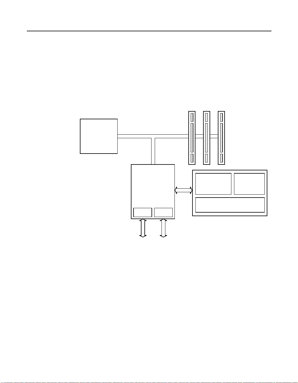
Figure 1.1 LSI53C1510 Block Diagram
32-Bit,
33 MHz
PCI Bus
132 Mbytes
160 Mbytes,
Memory
Interface
DRAM
DRAM
PCI
Interface
32-Bit
Memory
Controller
1-2 Introduction
Message
32-Bit RISC
ARM7TDMI
Processor
RAID
Parity Assist
Engine
I
2
Unit
O
SCSI
Core
SCSI
Core
80 Mbytes
Wide
Ultra2
SCSI Bus
80 Mbytes
Page 17

1.2 Module Overviews
This section provides an overview of the six major LSI53C1510 modules,
which consist of the PCI Interface, Memory Controller, I2O Messaging
Unit, ARM7TDMI RISC Processor, RAID PAE and SCSI Cores.
Chapter 2, “Functional Description,”provides a detailed description of the
functions of each module.
1.2.1 PCI Interface
The PCI interface is a 32-bit, 33 MHz host PCI bus. The PCI interface
supports Dual Address Cycle (DAC), PCI Power Management, and
Subsystem Vendor ID. The PCI interface also contains a PCI Master and
Slave control block, PCI configuration registers, and DMA channel
arbitration. This chip supports 64-bit addressing as a PCI master and
supports 32-bit addressing as a PCI slave.
1.2.2 Memory Controller
The memory controller provides access to Flash ROM, SRAM, and
32-bit EDO DRAM with parity (50 ns access time). It supports two
64 Mbytes (maximum configuration of 128 Mbytes) banks of DRAM. To
support the ROM and SRAM, there is a general purpose 8-bit expansion
memory bus that supports up to 4 Mbytes Flash ROM. It also supports
up to 2 Mbytes of SRAM and is designed to interface efficiently to an
external 8 K x 8 battery backed up SRAM.
1.2.3 I2O Message Unit
The messaging interface efficiently passes messages between the
LSI53C1510 and other I/O agents in an I2O enabled system. The
I2O Message Unit consists of the following four hardware FIFOs for the
message queuing lists: Request Free, Request Post, Reply Free, and
Reply Post. The LSI53C1510 provides control logic for the I2O Message
Unit and external local memory provides storage for the messages.
Module Overviews 1-3
Page 18

1.2.4 ARM7TDMI RISC Processor
The LSI53C1510 uses an optimized 32-bit ARM7 RISC Processor core
to control all RAID functionality. This frees the host CPU for other
processing activity and improves I/O performance. The RISC processor
and associated firmware contain the ability to manage an I/O from start
to finish without host intervention. The RISC processor also manages the
I2O message passing I/O interface.
1.2.5 RAID Parity Assist Engine (PAE)
The Hardware PAE offloads the parity generation and checking from the
host. It allows multiple parity operations to be queued for maximum
efficiency.
1.2.6 SCSI Cores
The integrated SCSI cores are high-performance dual wide Ultra2 SCSI
channels supporting either Single-Ended (SE) or Low Voltage Differential
(LVD) SCSI. The cores are based on the popular LSI53C8XX controllers
and are capable of up to Ultra2 transfer rates for each channel.
1.3 LSI53C1510 Features
The LSI53C1510 integrates a PCI bus master DMA core, two
high-performance SCSI cores, and two LSI Logic SCSI SCRIPTS™
processors to meet the broad requirements of Wide Ultra2 SCSI
standards. It is designed to implement multithreaded I/O algorithms with
a minimum of processor intervention, solving the protocol overhead
problems of previous intelligent and nonintelligent controller designs.
In nonintelligent mode, the LSI53C1510 is fully supported by the Storage
Device Management System (SDMS™), a software package that
supports the Advanced SCSI Protocol Interface (ASPI). SDMS software
provides BIOS and driver support for hard disk, tape, removable media
products, and CD-ROM under the major PC operating systems.
1-4 Introduction
Page 19

In intelligent mode, the LSI53C1510 is a complete, single chip RAID
solution for the motherboard—just add memory. The RAID product
solution consists of a RAID SYMplicity Storage Manager, SYMplicity
I2O RAID firmware with Wind River System IxWorks, and hardware.
1.3.1 Features List
• Highly integrated single chip RAID Controller
• I
• RAID PAE
• 32-bit/33 MHz host PCI Bus
• Two wide Ultra2 SCSI Channels
• 32-bit RISC ARM7TDMI Processor
• 32-bit Memory Controller
O Messaging Unit
2
–DAC
– PCI Power Management
– PCI cache commands (MRL, MRM, MWI)
– SE or LVD SCSI
– Based upon the popular LSI53C8XX controller
– Up to two banks of 64 Mbytes EDO (50 ns access time) DRAM
• General purpose 8-bit expansion bus
– Supports up to 4 Mbytes ROM
– Chip enable to support an external 8 K x 8 battery backed SRAM
1.4 LSI53C1510 Benefits
This section provides a description of the major LSI53C1510 benefits.
1.4.1 Ultra2 SCSI Benefits
Ultra2 SCSI is an extension of the SPI-2 draft standard that allows faster
synchronous SCSI transfer rates and defines a new physical layer, LVD
SCSI, that provides an incremental evolution from SCSI-2 and Ultra
SCSI. When enabled, Ultra2 SCSI (8-bit) performs transfers of
LSI53C1510 Benefits 1-5
Page 20

40 Mbytes/s, which results in approximately double the synchronous
transfer rate of Ultra SCSI. The LSI53C1510 can perform 16-bit (wide),
Ultra2 SCSI synchronous transfers as fast as 80 Mbytes/s. This
advantage is most noticeable in heavily loaded systems, or large block
size applications such as video on-demand and image processing.
An advantage of Ultra2 SCSI is that it significantly improves SCSI
bandwidth while preserving existing hardware and software investments.
1.4.2 LVDlink™ Benefits
The LSI53C1510 supports LVD SCSI, a signaling technology that
increases the reliability of SCSI data transfers over longer distances than
supported by SE SCSI. The low current output of LVD allows the I/O
transceivers to be integrated directly onto the chip. LVD provides the
reliability of High Voltage Differential (HVD) SCSI without the added cost
of external differential transceivers. Ultra2 SCSI with LVD allows a longer
SCSI cable and more devices on the bus, with the same cables defined
in the SCSI-3 parallel interface standard for Fast-20 (Ultra SCSI). LVD
provides a long-term migration path to even faster SCSI transfer rates
without compromising signal integrity, cable length, or connectivity.
For backward compatibility to existing SE devices, the LSI53C1510
features universal LVDlink transceivers that can switch between LVD
SCSI and SE modes. The LVDlink technology also supports high power
differential signaling in legacy systems, when external transceivers are
connected to the LSI53C1510. This allows the LSI53C1510 to be used
in both legacy and Ultra2 SCSI applications.
1.4.3 TolerANT®Technology Benefits
The LSI53C1510 features TolerANT technology, which includes active
negation on the SCSI drivers and input signal filtering on the SCSI
receivers. Through active negation, the SCSI Request, Acknowledge,
Data, and Parity signals are actively driven high rather than passively
pulled up by terminators. Active negation is enabled by setting bit 7 in
the STEST3 register.
TolerANT receiver technology improves data integrity in unreliable
cabling environments, where other devices are subject to data corruption.
TolerANT receivers filter the SCSI bus signals to eliminate unwanted
transitions, without the long signal delay associated with RC-type input
1-6 Introduction
Page 21

filters. This improved driver and receiver technology helps eliminate
double clocking of data, the single biggest reliability issue with SCSI
operations. TolerANT input signal filtering is a built-in feature of the
LSI53C1510 and all LSI Logic fast SCSI, Ultra SCSI, and Ultra2 SCSI
devices.
The benefits of TolerANT technology include increased immunity to noise
on the deasserting signal edge, better performance due to balanced duty
cycles, and improved Ultra2 SCSI transfer rates. In addition, TolerANT
SCSI devices do not cause glitches on the SCSI bus at power-up or
power-down, so other devices on the bus are also protected from data
corruption. TolerANT technology is compatible with both the Alternative
One and Alternative Two termination schemes proposed by the American
National Standards Institute.
1.4.4 I2O Benefits
The I2O-ready design of the LSI53C1510 improves system performance
by reducing interrupts to the host CPU and minimizing PCI bandwidth
through the packetized mailbox interface. These features are particularly
important in high-performance symmetric multiprocessing servers and
clustered computing systems. The benefits of the I2O architecture fully
compliment those of SCSI and include reduced host CPU I/O overhead
for better system performance, improved scalability, reduced time to
market for new I/O technology, reduced cost of integration and support
for I/O.
1.4.5 PAE Benefits
When the LSI53C1510 is in intelligent mode, the embedded PAE works
with RAID applications to perform parity generation or checking as
requested. The PAE writes any generated parity data block back into
local memory. The hardware PAE offloads the parity generation and
checking from the host and it generates parity faster than software
applications. The PAE allows multiple parity operations to be queued for
maximum efficiency. This frees the host CPU for other processing activity
and improves I/O performance.
LSI53C1510 Benefits 1-7
Page 22

1.4.6 ARM7TDMI RISC Processor Benefits
The ARM processor manages the I2O message passing I/O interface.
The embedded RISC processor (ARM7TDMI) improves system
performance by reducing interrupts to the host CPU and minimizing PCI
bandwidth. The ARM processor and associated software contain the
ability to manage an I/O from start to finish without host intervention. This
frees the host CPU for other processing activity and improves I/O
performance.
1.5 LSI53C1510 Benefits Summary
This section provides a summary of the PCI, SCSI, and RAID
performance benefits. It also provides a summary of the Testability,
Integration, and Reliability benefits.
1.5.1 PCI Performance
• Fully PCI 2.1 Specification compliant
• True multifunction device as defined in PCI 2.1 Specification in
nonintelligent mode and it presents only one load to the PCI bus
• Supports 32-bit word data bursts with variable burst lengths of 2, 4,
8, 16, 32, 64 or 128 Dwords across the PCI bus
• Prefetches up to 8 Dwords of SCSI SCRIPTS
• Performs zero wait-state bus master data bursts at 132 Mbytes/s
(@ 33 MHz)
• Supports PCI Cache Line Size register
• Supports PCI Memory Write and Invalidate, Memory Read Line, and
Memory Read Multiple commands
1.5.2 SCSI Performance
• Includes 4 Kbytes internal RAM on each SCSI channel for SCRIPTS
instruction storage, thus reducing PCI bus utilization
• Wide Ultra SCSI SE Interface
• Performs Wide Ultra2 SCSI synchronous transfers as fast as
80 Mbytes/s with LVD
1-8 Introduction
Page 23

• 816-byte DMA FIFO for more effective PCI and SCSI bus utilization
• SCSI synchronous offset of 31 levels for maximum performance in
long cable situations
• Supports variable block size and scatter/gather data transfers
• Minimizes SCSI I/O start latency
• Performs complex bus sequences without interrupts, including
restore data pointers
• Reduces ISR overhead through a unique interrupt status reporting
method
• Load/Store SCRIPTS instruction increases performance of data
transfers to and from chip registers
• Supports target disconnect and later reconnect with no interrupt to
the system processor
• Supports multithreaded I/O algorithms in SCSI SCRIPTS with fast
I/O context switching
• Expanded register Move instruction support
• Software (drivers and SCRIPTS) compatible with LSI53C8XX
• Integrated clock quadrupler enables Ultra2 SCSI with 40 MHz SCSI
clock input
1.5.3 RAID Performance
• Maximum transfer rate: 80 Mbytes/s with Wide Ultra2 SCSI
• Number of drives: 30 maximum (10 to 15 drives in typical application)
• Supports RAID levels 0, 1, 3, 5, 10 and JBOD
1.5.4 Testability
• Access to all SCSI signals through programmed I/O
• SCSI loopback diagnostics
• SCSI bus signal continuity checking
• Single-step mode operation
LSI53C1510 Benefits Summary 1-9
Page 24

1.5.5 Integration
1.5.6 Reliability
• Dual Channel SCSI Multifunction Controller
• 3.3 V/5 V PCI interface
• Full 32-bit PCI DMA bus master
• High-performance SCSI cores
• Integrated SCSI SCRIPTS processors
• ARM7TDMI 32-bit RISC processor
• RAID PAE
• I
O Message Unit
2
• 2 kV ESD protection on SCSI signals
• Typical 300 mV SCSI bus hysteresis
• Protection against bus reflections due to impedance mismatches
• Controlled bus assertion times (reduces RFI, improves reliability, and
eases FCC certification)
• Latch-up protection greater than 150 mA
• Voltage feed-through protection (minimum leakage current through
SCSI pads)
• Power and ground isolation of I/O pads and internal chip logic
• TolerANT technology provides:
– Active negation of SCSI Data, Parity, Request, and Acknowledge
signals for improved fast SCSI transfer rates
– Input signal filtering on SCSI receivers improves data integrity,
even in noisy cabling environments
1-10 Introduction
Page 25
1.6 Applications
There are many different applications and configurations for the
LSI53C1510 I2O-Ready PCI RAID Ultra2 SCSI Controller. Figure 1.2
illustrates a typical LSI53C1510 embedded motherboard application.
Figure 1.3 illustrates a typical LSI53C1510 host adapter board
application.
Figure 1.2 Typical LSI53C1510 Mainboard Applications
Host PCI
Bridge
32-bit, 33 MHz Primary PCI Bus
LSI53C1510
PCI to SCSI
I
O-Ready
2
RAID Controller
SCSI BSCSI A
Ultra2 SCSI Bus
1.6.1 Embedded Motherboard Application
The LSI53C1510 is ideally suited for embedded motherboard RAID
applications. The amount of motherboard space required to implement
such an application is critical. The limited space available on the
motherboard dictates a highly integrated solution like the LSI53C1510.
All of the major functional blocks of RAID controller including processor,
memory controller, XOR engine, and SCSI controllers are integrated into
the LSI53C1510. This greatly reduces the amount of board space
EDO DRAM
w/parity
(8–128 Mbyte)
8 Kbyte Battery Backed
SRAM w/RTC
Flash
(Up to
4 Mbyte)
Applications 1-11
Page 26
required to implement a RAID controller. Not only does this make RAID
on the motherboard a viable solution, it also greatly reduces the cost of
implementing it.
Because the LSI53C1510 supports both RAID and non-RAID operational
modes, it gives the motherboard designer the option of building a base
motherboard that uses the LSI53C1510 as a dual channel Ultra2 SCSI
controller. The additional memory and real time clock required for RAID
operation can then be provided on an optional RAID upgrade card that
plugs into a connector mounted on the motherboard.
Figure 1.3 Typical LSI53C1510 Host Adapter Board Application
VHDCI
Ultra2 SCSI Bus
VHDCI
Auto
Term
Auto
Term
Clock
NVRAM
68-pin
High Density
Ultra2 SCSI Bus
LSI53C1510
PCI to SCSI
I2O-Ready RAID
Controller
32-bit, 33 MHz PCI Bus
High Density
1.6.2 Host Adapter Board Application
The LSI53C1510 single chip RAID solution can be designed on an
add-in host adapter card. This provides a highly scalable solution where
additional storage and/or performance can be obtained by adding
additional host adapter cards.
68-pin
Battery Backed
SRAM
(8 K x 8) w/RTC
Flash
(2 to 4 Mbyte)
EDO DRAM
w/parity
(8 to 128 Mbyte)
Memory
Back-up
1-12 Introduction
Page 27

Chapter 2
Functional Description
The chapter contains the following sections:
• Section 2.1, “Modes of Operation,” page 2-2
• Section 2.2, “The Host Interface,” page 2-11
• Section 2.3, “LSI53C1510 Protocol Engine,” page 2-16
• Section 2.4, “Support Components,” page 2-18
The LSI53C1510 contains an ARM7 32-bit RISC Processor, a RAID
PAE, and a DMA engine. The RISC processor frees the host CPU for
other processing activity and improves performance. The RISC
processor and associated software contain the ability to manage an I/O
from start to finish without host intervention. The RISC processor also
manages the I2O message passing I/O interface. The DMA engine
moves blocks of data between system memory and the LSI53C1510
local memory.
The LSI53C1510 uses a 32-bit PCI interface for communication with the
host CPUs and system memory. The host interface to the LSI53C1510
is designed to minimize the amount of PCI bandwidth required to support
I/O requests. A packetized message passing I/O interface is used to
reduce the number of single cycle PCI bus cycles. All data traffic across
the PCI bus occurs with zero wait-state bursts.
The intelligent LSI53C1510 architecture allows the host to specify I/Os at
a very high level. Complete SCSI functionality is provided in the
LSI53C1510, relieving the host CPU(s) from managing I/Os.
LSI53C1510 I2O-Ready PCI RAID Ultra2 SCSI Controller 2-1
Page 28

2.1 Modes of Operation
The LSI53C1510 has two modes of operation: intelligent or nonintelligent
mode. In intelligent mode, the LSI53C1510 functions as an embedded
RAID controller on a motherboard or as an add-in RAID host adapter
board. In nonintelligent mode the LSI53C1510 functions as a PCI to
SCSI dual channel wide Ultra2 controller. These modes are entered
during the initialization of the LSI53C1510 on power-up. The presence or
absence of external memory determines which mode is entered. In
intelligent mode, the LSI53C1510 uses its built-in ARM processor. In
nonintelligent mode, the ARM processor is disabled. Table 2.1 shows the
LSI53C1510 modes of operation.
Table 2.1 LSI53C1510 Modes
Modes External Memory Configurations
Intelligent I
Controller
Nonintelligent Dual
Channel Controller
O RAID
2
Yes RAID
No Dual Channel Wide
Ultra2 SCSI Controller
2-2 Functional Description
Page 29
2.1.1 LSI53C1510 Overview
Figure 2.1 LSI53C1510 Block Diagram
Host PCI Bus (32-bit, 33 MHz)
PCI Master and Slave Control Block, PCI Configuration Registers (1/2 sets), and DMA Channel Arbitration
Ultra2 SCSI Controller
8 Dword
SCRIPTS
Prefetch Buffer
816 Byte
DMA FIFO
SCSI FIFO and SCSI Control Block
SCRIPTS
Processor
LVDlink Drivers and Receivers
SCSI
4 Kbyte
SCRIPTS RAM
Operating
Registers
Wide Ultra2 SCSI Bus
(A Channel)
Figure 2.1 illustrates the major components of the LSI53C1510 controller.
A dual channel PCI interface function block provides slave access
steering between the two SCSI cores when operating in nonintelligent
mode.
Buffer Buffer
Serial
EEPROM
and Auto-
Configuration
I2O
Msg Unit
8 Kbyte ARM
Instruction/
Data Buffer
ARM RISC
Processor
Internal Module Bus
Parity
Assist
Engine
JTAG
DMA
DRAM
Engine
Slave
Flash ROM
JTAG
ARM Debug
2-Wire Serial
EEPROM Bus
Flash ROM/DRAM
Memory Bus
Memory
Control
External
Interrupt Pin
Ultra2 SCSI Controller
SCSI
8 Dword
SCRIPTS
Prefetch Buffer
Operating
Registers
4 Kbyte
SCRIPTS RAM
816 Byte
DMA FIFO
SCSI FIFO and SCSI Control Block
SCRIPTS
Processor
LVDlink Drivers and Receivers
Wide Ultra2 SCSI Bus
(B Channel)
The Slave Access and Messaging Unit utilizes a FIFO for fast host
system service and for speed matching between the 33 MHz domain of
the PCI bus and the 40 MHz clock domain of the memory controller. The
DMA unit contains a single data FIFO for both read and write operations.
The SCSI cores each contain control registers and 4 Kbytes SCRIPTS
RAM. When operating in nonintelligent mode, these are mapped
Modes of Operation 2-3
Page 30

according to the Memory 0 and Memory 1 Base Address registers. When
in intelligent mode, the control registers are mapped into Memory 0 Base
Address registers.
The PAE accesses data and parity in the LSI53C1510 local memory and
performs XOR operations to generate parity and data blocks. Multiple
sources can be specified for each operation and multiple operations can
be queued within the unit.
The memory controller includes a 32-bit with parity EDO DRAM interface,
plus an 8-bit utility interface supporting SRAM, Flash ROM, plus
user-defined external components.
2.1.2 Configuration and Initialization
The LSI53C1510 initializes as a nonintelligent dual channel SCSI
controller, or as an intelligent I/O Processor (IOP). External pins are
sensed at power-on and either nonintelligent mode or intelligent mode is
selected. The power-on mode also determines which set of PCI
configuration register values will be used. When in nonintelligent mode,
the LSI53C1510 is a dual function PCI device with two sets of
configuration registers. When in intelligent mode, the LSI53C1510 is a
single function device with a single set of PCI configuration registers.
The MEM_ADDR bus is used to determine power-on configuration.
During power-on, internal 25 µA pull-downs are activated. If desired,
these pull-downs can be overridden using 10 kΩ external pull-up
resistors. This will change the default power-up conditions of the part.
Table 2.2 shows the ROM size configurations the eight MEM_ADDR lines
generate. The eight MEM_ADDR lines control the following configuration
options. Options shown in Table 2.3 are enabled using pull-up resistors.
2-4 Functional Description
Page 31

Table 2.2 ROM Size Configurations
MEM_ADDR [3:0] Options
0000 16 Kbytes ROM Size (No external pull-ups)
0001 32 Kbytes ROM Size
0010 64 Kbytes ROM Size
0011 128 Kbytes ROM Size
0100 256 Kbytes ROM Size
0101 512 Kbytes ROM Size
0110 1024 Kbytes ROM Size
0111 2048 Kbytes ROM Size
1000 4096 Kbytes ROM Size
1001–1110 Reserved
1111 No ROM present
Table 2.3 Configuration Options
MEM_ADDR [4:9] Options
Bit 4 Disable boot
Bit 5 RAID_MODE, based on SIMM/memory population
Bit 6 Disables SCSI SCRIPTS RAM
Bit 7 Disables EEPROM downloads
Bit 8 Reserved
Bit 9 Channel B uses INTA instead of INTB
Modes of Operation 2-5
Page 32

2.1.3 I2O Overview
When the LSI53C1510 is in intelligent mode, the RISC processor
manages the I2O message passing I/O interface. I2O defines a standard
architecture for intelligent I/O, where low level interrupts are offloaded
from the host CPU to the ARM IOP designed specifically to handle I/O.
With support for message passing between multiple independent
processors, the I2O architecture relieves the host of interrupt intensive
I/O tasks, greatly improving I/O performance in high bandwidth
applications such as RAID. I2O imposes no restrictions on where layered
modules execute, providing support for single processor, multiprocessor
and clustered systems.
The I2O specification also defines a “split driver” model for creating
drivers that are portable across multiple OSs and host platforms.
Through the split driver model, I2O significantly decreases the number of
drivers required. OS vendors write a single I2O-ready driver for each
class of device, such as SCSI Peripheral Class or Random Block Storage
Class. Device manufacturers, like LSI Logic, write a single I2O software
program for each device, such as the LSI53C1510, which works for any
OS that supports I2O.
2.1.4 I2O Conceptual Overview
The split I2O drivers are composed of two parts: the Operating System
Services Module (OSM), that resides on and interfaces to the host OS;
and the Hardware Device Module (HDM), that resides on and interfaces
with the LSI53C1510 adapter to be managed by the driver. The HDM and
the Intermediate Service Module (ISM) are often referred to collectively
as DDMs. The ISM is a driver an independent software vendor can
supply to add value or a specialized function to the LSI53C1510. These
modules interface with each other through a communication system
comprised of two layers: a Message Layer that sets up a communication
session, and a Transport Layer that defines how information will be
shared. Much like a standard communications protocol, the Message
Layer resides on top of the Transport Layer.
2-6 Functional Description
Page 33

2.1.5 I2O Benefits
The I2O operating environment of the LSI53C1510 provides two main
advantages. First, it enables the system vendor, LSI Logic, to create an
I/O platform that can support a number of intelligent configurations. The
second advantage is the capability of stacked drivers, that enable a third
party software vendor to provide value added expansion capability,
independent of both the OS and the hardware. Figure 2.2 illustrates
various ways the LSI53C1510 can be configured.
Figure 2.2 Example of LSI53C1510 Physical Configurations
Host System
Disk
Drive
Disk
Drive
Disk
Drive
SCSI
Channel
A
SCSI Bus A
Processor
Disk
Drive
Disk
Drive
Disk
Drive
LSI53C1510
RISC
System Bus
IOP
Memory
(Shared
Memory)
Other
Modules
System Memory
Disk
Drive
Disk
Drive
SCSI
Channel
B
Disk
Drive
SCSI Bus B
Modes of Operation 2-7
Page 34

2.1.6 The I2O Communications Model
The communications model for the I2O architecture is a message
passing system. The communication model defines how two entities
exchange messages by using the Message Layer to set up a connection
and exchange data and control.
When the OSM is presented with a request from the host OS, it
translates the request into an I2O message and dispatches it to the
LSI53C1510 for processing. Upon completion of the request, the
LSI53C1510 dispatches the result back to the OSM by sending a
message through the I2O Message Layer. To the host OS, the OSM
appears just like any other device driver. See Section 2.2.1, “Messages,”
later in this chapter for more detail.
2.1.7 Operational Overview
After power-on, the LSI53C1510 is configured as either a nonintelligent
or intelligent controller. In intelligent mode, the LSI53C1510 initializes
from local ROM and then issues and responds to I2O messages
exchanged with the host system. Messages are decoded into local
actions, usually involving the transfer of data. Data may be moved
between the host system and the LSI53C1510 local memory through the
LSI53C1510’s DMA controller, or by the host system. The two SCSI
cores transfer data between disk and local memory or between disk and
host system memory.
2.1.8 System Interface
The LSI53C1510 architecture features a generic, message passing I/O
interface. The LSI53C1510 Protocol Engine provides a set of four
hardware FIFOs for Message Queuing between the LSI53C1510 and the
primary host (or other hosts and peers). The four FIFOs are:
• Request Free List
• Request Post List
• Reply Free List
• Reply Post List
These FIFOs are used to manage how/where messages are sent and
received.
2-8 Functional Description
Page 35

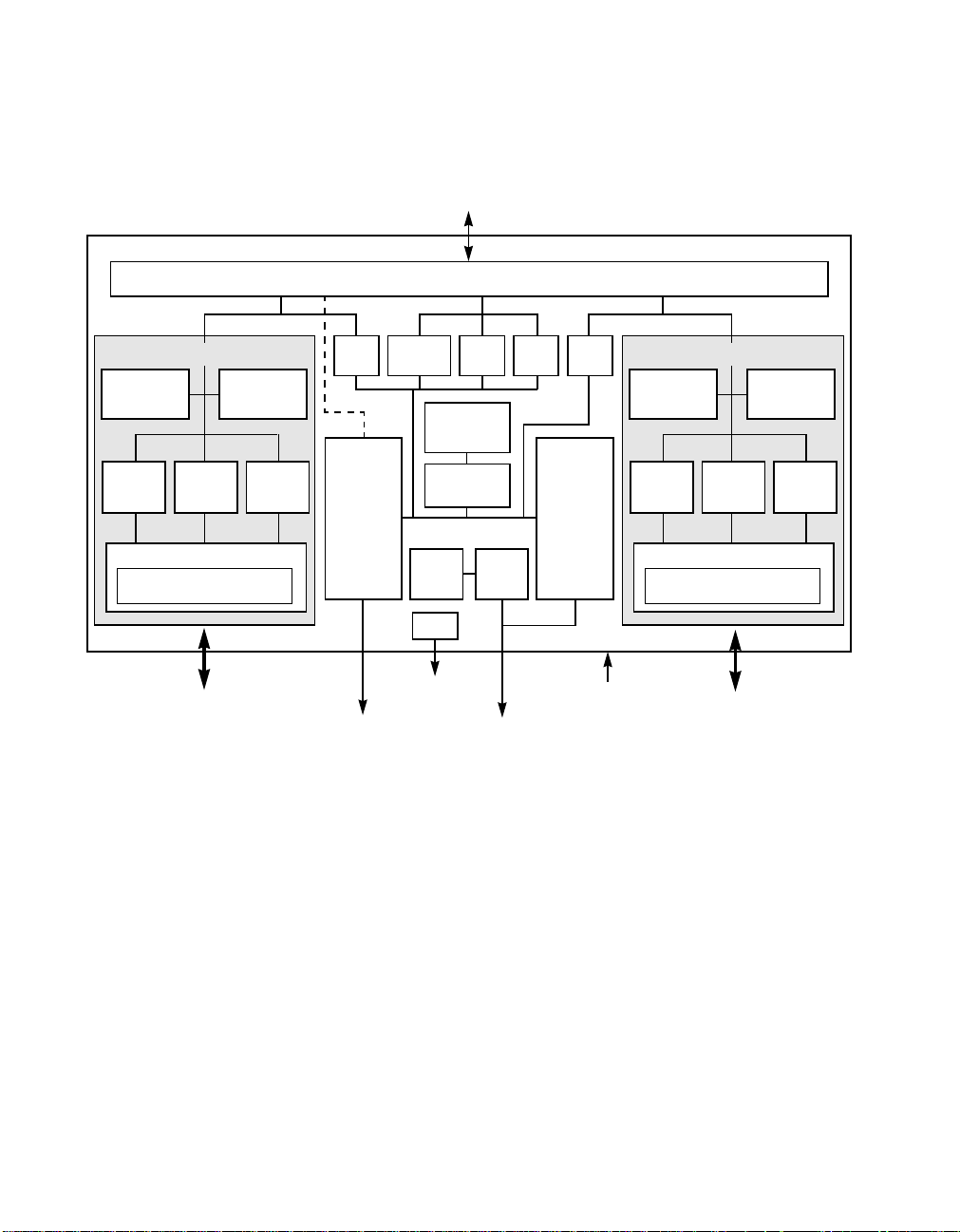
Control logic for the four hardware FIFOs is provided within the Protocol
Engine. Storage for the FIFO entries is provided in external local
memory. Each element within each of these FIFOs contains a Message
Frame Address (MFA). The MFA is the offset from the first memory base
address register (Memory 0 Base Address) where a Message Frame is
located (Push model). The number of FIFO elements is configurable.
Supported FIFO depths are powers of two between 256 and 4096.
In addition to the hardware FIFOs, a region of shared memory is
provided (the LSI53C1510 local memory mapped to System Addresses)
for the host to write Request Message Frames into. This is the default
method (Push model) for Request Message Frame transport, where the
host itself copies the Request Message Frame into the LSI53C1510 local
memory.
To support shared memory access (read/write), the LSI53C1510
Protocol Engine includes a slave burst FIFO (depth of 128 bytes), slave
burst logic including address capture and increment, and address
translation between System and Local memory addresses.
Reply Message Frames are always pushed from the LSI53C1510
Protocol Engine to System memory; the Protocol Engine includes a DMA
channel for transferring Reply Message Frames. This DMA channel may
also be used for other purposes such as downloading software or
uploading trace information. Also present within the Protocol Engine is a
System Read/Write interface which provides the ARM processor the
ability to read/write a single arbitrary Dword from system memory. See
Figure 2.3 for an illustration of the FIFOs and memory in the Protocol
Engine and External Memory.
2.1.8.1 LSI53C1510 Protocol Engine Overview
The LSI53C1510 Protocol Engine contains an ARM processor core, a
local bus and controller, an 8 Kbytes Instruction Cache, an 8 Kbyte
Instruction/Data Buffer, an External Memory Controller, an Instruction
Prefetch Unit, a write Buffer, an interface to the host system, and a
Timer/Control block. The LSI53C1510 Protocol Engine functions as an
intelligent IOP. It receives Request Messages from the host CPU,
processes them, and sends Reply Messages back to the host.
Processing of Request Messages typically involves an I/O transaction;
the Protocol Engine and associated software together contain the ability
to manage an I/O from start to finish without host intervention.
Modes of Operation 2-9
Page 36

Figure 2.3 Hardware Messaging Unit
Protocol Engine
PCI Interface
External Memory
Request Free List FIFO Control
Request Post List FIFO Control
Reply Free List FIFO Control
Reply Post List FIFO Control
Slave Burst FIFO
Master Burst FIFO
Request Free List FIFO Data
Request Post List FIFO Data
Reply Free List FIFO Data
Reply Post List FIFO Data
Shared Memory
(Request Message Frames)
Private Memory
(Code + Data)
2-10 Functional Description
Page 37

2.2 The Host Interface
The LSI53C1510 host interface is compliant with the I2O Specification,
Revision 1.5. This host interface is a high-performance, packetized,
mailbox architecture which leverages intelligence in the LSI53C1510 to
minimize traffic on PCI. See http:\\www.i2osig.org on the I2O Special
Interest Group (SIG) web site for more information.
SYMplicity is the LSI Logic implementation of I2O architecture. There are
two basic constructs in I2O. The first construct, the Message, is used to
communicate between the host and the LSI53C1510. Messages are
moved between the host(s) and the LSI53C1510 using the second
construct, a Transport mechanism.
2.2.1 Messages
The LSI53C1510 uses Request and Reply Messages to communicate
with the host. Request messages are created by the host to “request” an
action by the LSI53C1510. Reply messages are used by the
LSI53C1510 to send status information back to the host.
Request message data structures are 128 bytes in length. The message
includes a message header and a payload. The header includes
information to uniquely identify the message. The message header
information is sophisticated enough to support multiple hosts and targets.
The payload may be any one of three different mechanisms to
communicate scatter/gather information to the LSI53C1510.
2.2.2 Message Transport
Request and Reply Messages reside in preallocated message frames.
Message frames may reside in PCI shared memory local to the
LSI53C1510 or in host memory.
The host selects where the Request and Reply messages are located
during the LSI53C1510 initialization. The default, power-up configuration,
places Request messages in PCI shared memory local to the
LSI53C1510. As an option, the Request messages can reside in host
memory. The Reply messages, however, always reside in host memory.
The Host Interface 2-11
Page 38

Pointers that point to the Request and Reply Messages are called MFAs.
The LSI53C1510 is responsible for the initialization and management of
the MFAs in the default model. The LSI53C1510 includes a set of four
FIFOs which are used to track the Request and Reply MFAs. The four
FIFOs are:
• Request Free List
• Request Post List
• Reply Free List
• Reply Post List
Each element within the FIFOs contains the 32-bit MFAs. The Free List
FIFO contains MFAs to memory locations which are “free” to be used for
new messages. The LSI53C1510 first enters these MFAs into the
Request Free List FIFO at initialization. The Host initializes the Reply
Free List by writing the MFAs for the Reply messages into the Reply
Register. The act of writing to this register pushes the MFA into the FIFO.
The Post List FIFOs contain pointers to memory locations which contain
new messages. The presence of a MFA in the Post FIFO indicates to the
host or to the LSI53C1510 that a message is pending. The depth of the
FIFOs determines the number of outstanding Request Messages which
may be pending. The total number of outstanding or open I/Os is limited
by the number of Request Messages. Therefore, the maximum number
of open I/Os is determined by the size or depth of the FIFOs. The depth
of the FIFOs in the LSI53C1510 is software configurable, from 256 to
4096, in powers of two. The storage elements for the FIFO are in the
local DRAM external to the chip. Therefore, the size of the FIFOs will
have an impact on the total amount of DRAM required. See
Section 2.4.1, “DRAM Memory,” later in the chapter for more information
regarding local DRAM requirements.
2.2.3 Request Message
The LSI53C1510 maintains a list of pointers to memory structures. The
pool of pointers (MFAs) are stored in the LSI53C1510 Free FIFO. The
top FIFO entry is provided to the host driver by reading the LSI53C1510
Request Register. In the default operation, the LSI53C1510 provides
MFAs to the LSI53C1510 local memory, mapped as shared memory. The
2-12 Functional Description
Page 39

process of the host writing to shared memory local to the LSI53C1510 is
analogous to “pushing” messages down the PCI hierarchy to the
LSI53C1510. This process may be referred to as the Push model.
Alternatively, the LSI53C1510 may be configured to provide MFAs to
memory located on the host. Once configured as such, the LSI53C1510
will “pull” the messages to memory local to the LSI53C1510 using PCI
bus master cycles. This process may be referred to as the Pull model.
The LSI Logic I2O RAID software uses the Push model.
2.2.3.1 To Send a Request Message
Figure 2.4 illustrates the LSI53C1510 Request Message Transport.
1. The host driver reads the LSI53C1510 Request Register to retrieve
a pointer to the next available message structure. If the Message
structure resides in PCI shared memory local to the LSI53C1510 (the
default), the host reads the offset of the Message structure with
shared memory. Device drivers may be written to request several
pointers through a series of fast back-to-back PCI slave read cycles.
If there are no available message structures, Request Register reads
return the value of FFFF–0xFFFF.
2. The host driver then builds the Request Message(s) and writes the
contents to the available message structure(s).
3. When the Request Message is built, the host driver writes the
MFA(s) back to the LSI53C1510 Request Register. This action
creates a queued entry in the LSI53C1510 Post FIFO. Host drivers
may post several MFAs during fast back-to-back PCI write cycles.
4. The LSI53C1510 Protocol Engine is interrupted on the first post
creating a “Request Post FIFO Not Empty” condition.
5. The LSI53C1510 removes all of the MFAs from the Post FIFO.
6. If the LSI53C1510 is operating under the Pull model, then the
LSI53C1510 arbitrates for the PCI bus with the intent to copy the
Request Message(s) in host memory using burst read cycles to
memory local to the LSI53C1510. The LSI53C1510 will immediately
start operating on request message(s) already written to local PCI
shared memory, if it is operating in the Push model.
The Host Interface 2-13
Page 40

7. Finally, the LSI53C1510 frees the memory associated with the
message request by placing the MFA back in the Request Free FIFO.
If the operation requested by the Request Message requires a Reply
Message from the LSI53C1510 to the host, then a similar message
transfer process is initiated (see Section 2.2.4, “Reply Message”).
The host driver may choose to poll the Reply Messages or have the
LSI53C1510 interrupt on exception conditions.
Figure 2.4 LSI53C1510 Request Message Transport
MF_1
MF_2
MF_3
MF_N
REQUEST
Message Frames
2
MFA_1
MFA_2
MFA_N
Free FIFO
6
2.2.4 Reply Message
The Reply Queue provided by the LSI53C1510 is managed similarly,
except the LSI53C1510 generates the Reply Messages. The host has
the responsibility to allocate the Reply Message Pool, and post the MFA
of each message frame to the Reply Register.
2.2.4.1 To Send a Reply Message
Host Driver
1
1 3
Request Register
7
LSI53C1510
3
4
5
MFA_1
MFA_2
MFA_N
Post FIFO
Figure 2.5 illustrates the LSI53C1510 Reply Message Transport.
1. The LSI53C1510 retrieves a MFA to the next free message frame
from the Reply Message Free FIFO.
2. The LSI53C1510 then writes the message to the Reply Message
frame queue.
2-14 Functional Description
Page 41

3. When the Reply Message is written into the queue, the LSI53C1510
writes the pointer into the LSI53C1510 Post FIFO.
4. The LSI53C1510 Protocol Engine causes an interrupt to the host
when the Reply Message is posted.
5. The host driver reads the Reply Register to retrieve the Reply
Message pointer from the Post FIFO. If there are no posted
messages when the host reads the Reply Register, the host receives
the value FFFF–0xFFFF.
6. The host driver then retrieves the Reply Message.
7. Finally, the host driver writes the MFA (now a free message frame)
to the Reply Register.
Figure 2.5 LSI53C1510 Reply Message Transport
MFA_1
MFA_2
MFA_N
Free FIFO
7
4
1
2.2.4.2 The “Push” Model
The “Push” model for the data transfer defines the host’s “push” of
request messages down to the PCI shared memory local to the
LSI53C1510. The location to which the host writes is provided by the
Request Free List.
Host Driver
7
Reply Register
LSI53C1510
5
3
5
6
MFA_1
MFA_2
MFA_N
Post FIFO
MF_1
MF_2
MF_3
2
MF_N
REPLY
Message Frames
The Host Interface 2-15
Page 42

2.3 LSI53C1510 Protocol Engine
The LSI53C1510 provides a Protocol Engine to manage the execution of
various I2O protocols. The Protocol Engine offloads the host processor
from management of the I2O protocol by providing a higher level of
abstraction for the SCSI protocols. This abstraction allows multiple SCSI
protocols to operate simultaneously, with no coordination required
between the host-based drivers.
Each of the abstracted classes of service has well defined Request and
Reply Message protocols. The SYMplicity I2O RAID software supports
the Random Block Storage Class. This class provides a high level
abstraction for random access block-oriented storage devices.
2.3.1 Random Block Storage Class
The Random Block Storage Class provides a high level abstraction for
random access block-oriented storage media. The class definition
abstracts normal I/O operation using a message that consists of the
starting logical block address, the number of bytes, the data buffer, the
operation code, and the device handle on which to operate. The
LSI53C1510 optimizes the request processing by attempting to sort and
concatenate different requests, thereby reducing seek and latency time
on the drives, and overall command overhead per request. Each request
is managed as a single exchange and appropriate error recovery and
reporting is provided. Table 2.4 lists the base messages that comprise
the Random Block Storage Class message protocol.
2-16 Functional Description
Page 43

Table 2.4 Supported Random Block Storage Messages
Function Description
BsaBlockRead Read from device to memory
BsaBlockReassign Reassign block addresses
BsaBlockWrite Write to device from memory
BsaBlockWriteVerify Write to device from memory then verify
BsaCacheFlush Write dirty cache to media
BsaDeviceReset Reset the device
BsaMediaFormat Not defined at this time
BsaMediaVerify Verify accessibility of data
BsaPowerMgt Power Management
BsaStatusCheck Check device status
In addition to the base messages for each class, the class definitions
also provide utility messages to allow for management and configuration
of devices. A generic user interface scripting language is used to allow
for building generic configuration and management applications.
LSI53C1510 Protocol Engine 2-17
Page 44

2.4 Support Components
The memory controller block within the LSI53C1510 provides access to
external local memory resources. External memory devices supported
include Flash ROM, DRAM, and SRAM.
The sections below provide guidance in choosing the support
components necessary for a fully functional implementation using the
LSI53C1510. A LSI53C1510 typical implementation diagram is shown
below in Figure 2.6 for reference.
Figure 2.6 Typical Implementations
VHDCI
Ultra2 SCSI Bus
VHDCI
Auto
Term
Auto
Term
Clock
NVRAM
68-pin
High Density
Ultra2 SCSI Bus
LSI53C1510
PCI to SCSI
I2O-Ready RAID
Controller
32-bit, 33 MHz PCI Bus
68-pin
High Density
Battery Backed
SRAM
(8 K x 8) w/RTC
Flash
(2 to 4 Mbyte)
EDO DRAM
w/parity
(8 to 128 Mbyte)
Memory
Backup
2-18 Functional Description
Page 45

2.4.1 DRAM Memory
The DRAM memory stores a run time image of the LSI53C1510
software. This memory also provides a data cache for RAID operations.
The LSI53C1510 uses a 32-bit demultiplexed memory bus to access the
DRAM. This memory bus has the capability to address up to 128 Mbytes
of EDO DRAM. The memory controller managing this bus has the
flexibility to support variable DRAM access speeds. The speed of the
DRAMs will have a dramatic impact on the performance of the
LSI53C1510 and 50 ns EDO DRAM is required. The LSI53C1510
memory controller also supports optional byte-wide parity error detection.
2.4.2 Flash ROM
The memory controller in the LSI53C1510 manages an optional Flash
ROM. If present, the Flash ROM is used to store the software for the
LSI53C1510 Protocol Engine and INT 0x13 boot software.
If the Flash ROM is not used, then the host platform is responsible for
downloading the Protocol Engine software to the LSI53C1510 through
the PCI interface. The LSI53C1510 supports a diagnostic interface that
is enabled through a sequence of commands issued to the WRSEQ
register in the host interface register set. Software may be directly written
to the LSI53C1510 internal memory and external DRAM through the
diagnostic interface. Details of this implementation are not currently
defined; therefore, LSI Logic recommends using Flash ROM for software
storage.
The Flash ROM is accessed using the lower 8 bits of the DRAM Memory
Interface.
2.4.3 Serial EEPROM
The serial EEPROM is primarily used during nonintelligent mode
operations. It can be programmed using the host interface of the
LSI53C1510.
Support Components 2-19
Page 46

2-20 Functional Description
Page 47

Chapter 3
Software Description
This chapter describes the software features, firmware features, and
memory requirements for the LSI53C1510 in the following sections:
• Section 3.1, “PCI RAID Software Solutions,” page 3-1
• Section 3.2, “Management Software Features,” page 3-3
• Section 3.3, “RAID Firmware Features,” page 3-3
• Section 3.4, “SDMS Software,” page 3-8
• Section 3.5, “Memory Requirements,” page 3-8
3.1 PCI RAID Software Solutions
The LSI53C1510 is the first in high-integration RAID processor. LSI Logic
offers a full PCI RAID software solution consisting of the LSI Logic RAID
DDM, SYMplicity Storage Manager utility, and Wind River Systems’
IxWorks RTOS. These applications run in the LSI53C1510 intelligent
mode.
3.1.1 PCI RAID
Operating in intelligent mode, the LSI53C1510 can use the LSI Logic PCI
RAID software package.
Leveraging third generation software from the LSI Logic established and
successful bridge controllers and subsystems, the LSI Logic RAID
software for the LSI53C1510 provides an extremely stable, feature rich,
high availability platform.
LSI53C1510 I2O-Ready PCI RAID Ultra2 SCSI Controller 3-1
Page 48

3.1.2 SYMplicity Storage Manager
SYMplicity Storage Manager provides host-based, transparent
management of disk array controllers and the following features.
• Common Features
– Obtaining a RAID Module Profile
– Naming a RAID Module (user-defined)
– Locating a RAID Module
• Configuration
– LUN creation, deletion using GUI or command line
– Easy default configurations or detailed parameter options
available
– Manages multiple RAID modules
– Hot Spare Creation/Deletion
– Dynamic Reconfiguration features
• Status
– Event logging in system log or Storage Manager (specific log)
– Scriptable error notification_SNMP, email, etc.
– LUN Reconstruction progress and in-progress tuning
– Performance Monitor
◊ GUI displays key statistics for a card and its logical units
◊ Command line interface captures full set of detailed data
• Recovery
– Health Check for immediate report of component failures
– Lead-through Recovery Steps from Single or Multiple Failures
• Maintenance/Tuning
– Cache Management
– Parity Check and Repair
– Set LUN Reconstruction Rates
3-2 Software Description
Page 49

3.1.3 Wind River Systems’ IxWorks RTOS
Wind River Systems has ported IxWorks to the LSI53C1510. This
version of IxWorks has been tuned for optimal performance.
3.2 Management Software Features
Management software has the following features:
• Supported by SYMplicity Storage Manager
• Client/Server Model (Windows NT/Win95 Client with Windows NT,
Netware, or UNIXWare Server)
• Compatible with Microsoft Cluster Server (Wolfpack)
• Online maintenance and event notification
• BBU Support with Utility level software
• Remote Diagnostic Capability
• Configurable Drive Rebuild rate
• Recovery Guru
3.3 RAID Firmware Features
RAID firmware has the following features:
• RAID Levels 0, 1, 3, 5, and 10
• Caching
– Caching (Read-ahead, write through, or write back)
– Cache memory options of 8 Mbyte to 128 Mbyte
• Runs in optimal and degraded mode
• Hardware Assisted Parity Calculation
• Variable Stripe Size
• Tagged Command Queuing
• Global hot spare drives
• Drive hot swap with automatic, transparent reconstruction
Management Software Features 3-3
Page 50

• Online Dynamic Capacity Expansion
• Online RAID Level Migration/Reconfiguration
• Battery Backup Support and Cache Recovery
• Supports SCSI Accessed Fault-Tolerant Enclosure (SAF-TE)
3.3.1 RAID Levels 0, 1, 3, 5, and 10
This section describes RAID and the different RAID levels.
3.3.1.1 RAID (Redundant Array of Independent Disks)
A disk array in which part of the storage capacity is used to store
redundant information about user data stored on the remainder of the
storage capacity. The redundant information enables regeneration of
user data if one of the disk drives in the drive group fails.
3.3.1.2 RAID Level
Indicates the way the controller reads and writes data and array parity
on the drives. The LSI53C1510 controller can create RAID Level 0, 1, 3,
and 5 logical units. These levels DO NOT indicate any certain hierarchy
or preference.
3.3.1.3 RAID Level 0
RAID Level 0 is a nonredundant RAID Level where data, without parity,
is striped across a drive group/LUN. All drives are available for storing
user data. Any single drive failure causes data loss and a logical unit
status of Dead.
3.3.1.4 RAID Level 1
RAID Level 1 or disk mirroring, protects data against disk failure by
replicating all data stored on the virtual disk at least once. For some I/O
intensive applications, a RAID Level 1 can improve performance
significantly over a single disk. As implemented by LSI Logic, RAID 1
combines both striping and mirroring. The striping and mirroring
combination is also referred to as RAID 0+1 or RAID 10.
3-4 Software Description
Page 51

3.3.1.5 RAID Level 3
RAID Level 3 adds parity to a striped array, permitting user data to be
regenerated in the event of a failure. RAID Level 3 arrays use normal disk
mechanisms for failure detection and the parity for data regeneration in
the event of a failure. RAID Level 3 relies on close coordination of
member disk activities.
3.3.1.6 RAID Level 5
RAID Level5 is another independent access RAID Level. It is functionally
equivalent to RAID Level 4, using a single parity strip to protect data
stored on severaldata strips in the same stripe. It differs from RAID Level
4 in that its parity strips are distributed across multiple array members
rather than being concentrated on a dedicated parity disk. This provides
some relief from the write bottleneck that characterizes RAID Level 4,
and is the reason that RAID 5 is most often implemented in independent
access RAID array products rather than RAID Level 4.
3.3.2 Caching
Cache memory is an area on the controller used for intermediate storage
of read and write data. By using cache, you can increase system
performance because the data for a read or write operation from the host
may already be in the cache from a previous operation (thus the need to
access the drive itself is eliminated), or the write operation is considered
complete once it is written to the cache. The following caching options
are supported.
• Caching (Read-ahead, write through, or write back)
• Cache memory options of 8 Mbyte to 128 Mbyte
3.3.3 Runs in Optimal and Degraded Mode
The software permits your RAID system to produce optimal performance.
If a failure occurs, the system can run in a degraded mode until
replacement of the failed unit occurs.
RAID Firmware Features 3-5
Page 52

3.3.4 Hardware Assisted Parity Calculation
RAID firmware uses the Hardware PAE in the LSI53C1510 to offload
parity generation and checking from the host. The PAE calculates the
parity for write operations much faster than what can be done in
software/firmware. It also allows multiple parity operations to be queued
for maximum efficiency.
3.3.5 Tagged Command Queuing
Tagged command queuing provides the capability for the host to issue
multiple commands to a logical unit. This capability is essential for an
array logical unit that is made up of multiple devices. Without tagged
queuing, the controller can only execute one operation on the logical unit
at a time, even though there are multiple drives available for overlapped
operations. The maximum number of commands which can be queued
in the controller (the sum of all logical units) is 256. This is the number
of available structures the controller has for operations received from the
host. If the host attempts to issue more commands to the controller than
it has structures available for, a Queue Full status will be returned.
The controller maintains a queue for each logical unit and a queue for
each drive in the logical unit. How a command moves from queue to
queue is dependent on the type of queue tag received with the
command.
3.3.6 Global Hot Spare Drives
This drive contains no valid data but if a failure occurs, the controller can
automatically reconstruct and use the global hot spare drive to replace a
failed drive. Hot spare drive allows full performance and data redundancy
to be restored without user intervention. The user simply replaces the
failed drive at a later time. This is an important feature because it can
significantly reduce mean time to data loss. A global hot spare drive can
replace a failed drive of the same or smaller capacity anywhere on the
disk array.
3-6 Software Description
Page 53

3.3.7 Hot Swap Drive with Automatic, Transparent Reconstruction
This disk drive replaces a failed drive. Hot Swap technology makes it
possible to remove and replace an array component while power is
applied and data activity to and from the system continues. The controller
automatically reconstructs data on the new drive, or initiates copying
back the data from the global hot spare drive that is standing in for the
failed drive. This data reconstruction is transparent to the user and allows
full performance and data redundancy to be restored.
3.3.8 Variable Stripe Size
The Dynamic Segment Sizing (DSS) feature provides the ability to
change the segment size for a LUN. Changing the segment size causes
the LUN to be reconfigured such that the data is mapped according to
the new segment size. This feature is provided while allowing full user
data availability and accessibility. The RAID firmware allows variable
stripe size. A striped array is also known as a RAID Level 0 array.
3.3.9 Online Dynamic Capacity Expansion
The Dynamic Capacity Expansion feature provides the ability to add
drives to a drive group. Adding drives to a drive group causes the LUNs
on that drive group to be reconfigured such that the data is spread onto
the additional drives.After reconfiguration, the additional capacity may be
used to create additional LUNs on the drive group. This feature is
provided while allowing full user data availability and accessibility.
3.3.10 Online RAID Level Migration/Reconfiguration
The Dynamic RAID Migration (DRM) feature provides the ability to
change the RAID Level for a drive group. Changing the RAID Level
causes the LUNs in the drive group to be reconfigured such that the data
is mapped according to the definition of the new RAID Level. This feature
is provided while allowing full user data availability and accessibility. Valid
RAID Level Migrations are: 0>1, 0>3, 0>5, 1>0, 1>3, 1>5, 3>0, 3>1, 3>5,
5>0, 5>1, and 5>3.
RAID Firmware Features 3-7
Page 54

3.3.11 Battery Backup Support and Cache Recovery
The Battery Backup feature allows data in cache memory to be saved
and then recovered following a power failure.
3.3.12 Supports SAF-TE
SAF-TE support has been added to the destination (drive) side of the
controller. This allows attachment of drive enclosures that support
SAF-TE.
3.4 SDMS Software
Operating in nonintelligent mode, the LSI53C1510 can use the SDMS
software package.
SDMS software is a complete software package that solves the
increasingly complex problem of managing system I/O. It seamlessly
addresses hardware and software interfaces by supporting the LSI Logic
family of SCSI processors and controllers, and a wide range of SCSI
peripheral devices, while offering interoperability across application
programs, operating systems, and host platforms. SDMS software
consists of a resident SCSI BIOS that manages all SCSI controller or
processor specific functions, and a series of SCSI device drivers that
provide operating system and peripheral specific support.
SDMS software provides a standard method to interface SCSI I/O
subsystems with devices, operating systems, and application software. It
also enhances system capabilities already provided by SCSI controllers
and processors by facilitating multithreaded I/O support, system wide
SCSI device access, and the creation of new applications.
3.5 Memory Requirements
To run the LSI53C1510 in intelligent mode, with the PCI RAID software
solutions (LSI Logic RAID DDM, SYMplicity Storage Manager utility, and
Wind River Systems’ IxWorks RTOS), your memory should meet the
following requirements.
3-8 Software Description
Page 55

• EDO DRAM (with parity) - 8 Mbytes to 128 Mbytes
• Flash ROM - minimum of 2 Mbytes
• NVRAM (with real time clock) - 8 Kbytes
(equivalent to SGS-Thomson MK48T18)
To run the LSI53C1510 in nonintelligent mode, with LSI Logic the SDMS
software package, your memory should meet the following requirements.
• Two Serial EEPROM - 2 Kbytes
• Flash ROM - 128 Kbytes
Memory Requirements 3-9
Page 56

3-10 Software Description
Page 57

Chapter 4
Signal Descriptions
This chapter presents the LSI53C1510 pin configuration and signal
definitions using tables and illustrations. Figure 4.1 is the functional
signal grouping. The signal descriptions are organized into functional
groups:
• Section 4.1, “Signal Groupings,” page 4-2
• Section 4.2, “PCI Interface Signals,” page 4-4
• Section 4.3, “SCSI Interface Signals,” page 4-10
• Section 4.4, “Memory Interface Signals,” page 4-15
• Section 4.5, “Miscellaneous Interface Signals,” page 4-18
A slash (/) at the end of a signal name indicates that the active state
occurs when the signal is at a LOW voltage. When the slash is absent, the
signal is active at a HIGH voltage.
All signals/pins described in this chapter are identified by a pin type
described in Table 4.1.
Table 4.1 Pin Type Description
Type Description
I Input, a standard input only signal
O Totem Pole Output, a standard output driver
I/O Input and Output (bidirectional)
T/S 3-state, a bidirectional, 3-state input/output signal
S/T/S Sustained 3-state, an active LOW 3-state signal
LSI53C1510 I2O-Ready PCI RAID Ultra2 SCSI Controller 4-1
owned and driven by one and only one agent at a
time
Page 58

4.1 Signal Groupings
The LSI53C1510 signals fall into the following groups. These groups are
illustrated in Figure 4.1.
• PCI Interface Signals
– System Signals
– Address and Data Signals
– Interface Control Signals
– Arbitration Signals
– Interrupt Signals
– Error Reporting Signals
– Power Management Event Signals
• SCSI Interface Signals
– A-Channel
– B-Channel
• Memory Interface Signals
– ROM/SRAM Signals
– EDO DRAM Signals
• Miscellaneous Interface Signals
– SCSI GPIO Function Signals
– UART Signals
– JTAG Signals
– ARM Debug Signals
– ARM
– RAID Mode
• Power and Ground Signals
4-2 Signal Descriptions
Page 59

Figure 4.1 LSI53C1510 Functional Signal Groupings
PCI
Bus
Interface
32-bit
33 MHz
Memory
Interface
System
Address
and
Data
Interface
Control
Arbitration
Interrupt
Error
Reporting
Power
Management
Event
ROM
SRAM
Signals
EDO
DRAM
Signals
CLK
LSI53C1510
RST/
PCI_AD[31:0]
C_BE[3:0]/
PAR
A_SCTRL/
FRAME/
TRDY/
IRDY/
STOP/
DEVSEL/
IDSEL/
REQ/
GNT/
INTA/
INTB/
SERR/
PERR/
PME/
B_SCTRL/
MCE2_RD/
MCE2_WR/
MEM_CE[2:0]
MEM_WE/
MOE/_TESTOUT
MEM_ADDR[12:0]
MEM_DATA[7:0]
SCANMODE
SCAN_EN
SCAN_RAM_EN
SCAN_RST_EN
SCAN_TEST_CLK_EN
TEST_HSC
TEST_DRAMCLK
TESTIN
DRAM_CASFB_A
DRAM_CASFB_B
DRAM_WE/
DRAM_OE/
DRAM_ADDR[12:0]
DRAM_DATA[31:0]
DRAM_PAR[3:0]
DRAM_RAS/[3:0]
DRAM_CAS/[7:0]
A_SD[15:0] /
A_SDP[1:0] /
A_SC_D /
A_SI_O /
A_SMSG /
A_SREQ /
A_SACK /
A_SBSY /
A_SATN /
A_SRST /
A_SSEL /
A_DIFFSENS
A_RBIAS
SCLK
B_SD[15:0] /
B_SDP[1:0] /
B_SC_D /
B_SI_O /
B_SMSG /
B_SREQ /
B_SACK /
B_SBSY /
B_SATN /
B_SRST /
B_SSEL /
B_DIFFSENS
B_RBIAS
A_GPIO[4:0]
B_GPIO[4:0]
RXT
TXT
TCK
TMS
TDI
TDO
TRST/
ARM_TMS
ARM_TDO
ARM_TRST/
XINT
POWER_FAIL/
SCSI LVD
Channel
A
SCSI
Interface
SCSI LVD
Channel
B
SCSI
GPIO
Functions
UART
JTAG
Misc.
Interface
ARM
Debug
ARM
RAID Mode
Signal Groupings 4-3
Page 60

4.2 PCI Interface Signals
The PCI Bus Interface Signals section contains tables describing the
signals for the following signal groups: System Signals, Address and
Data Signals, Interface Control Signals, Arbitration Signals, Interrupt
Signals, the ARM Signal, Error Recording Signals, the Power
Management Signal, and GPIO Interface Signals.
4.2.1 System Signals
Table 4.2 describes the System signals.
Table 4.2 System Signals
Name Bump Type Strength Description
CLK F25 I N/A Clock provides timing for all transactions on the PCI bus and
RST/ N24 I N/A Reset forces the PCI sequencer of each device to a known
is an input to every PCI device. All other PCI signals are
sampled on the rising edge of CLK, and other timing
parameters are defined with respect to this edge. Clock can
optionally serve as the SCSI core clock, but this may effect fast
SCSI transfer rates.
state. All T/S and S/T/S signals are forced to a high impedance
state, and all internal logic is reset. The RST/ input is
synchronized internally to the rising edge of CLK. The CLK
input must be active while RST/ is active to properly reset the
device.
4-4 Signal Descriptions
Page 61

4.2.2 Address and Data Signals
Table 4.3 describes the Address and Data signals.
Table 4.3 Address and Data Signals
Name Bump Type Strength Description
PCI_AD[31:0] M25, M24, M26,
L25, L24, L26, K23,
K25, J25, H25, J24,
H26, H23, G25,
G26, H24, C25,
D24, A25, C23, B24,
A24, D22, B23, B22,
A22, D20, B21, A21,
C21, B20, A20
C_BE[3:0]/ K26, G23, E24, A23 T/S 16 mA
PAR C26 T/S 16 mA
T/S 16 mA
PCI
PCI
PCI
Physical dword PCI Address and Data are
multiplexed on the same PCI pins. During
the first clock of a transaction, AD[31:0]
contain a physical byte address. During
subsequent clocks, AD[31:0] contain data.
A bus transaction consists of an address
phase followed by one or more data
phases. PCI supports both read and write
bursts. AD[7:0] define the least significant
byte, and AD[31:24] define the most
significant byte.
Bus Command and Byte Enables are
multiplexed on the same PCI pins. During
the address phase of a transaction,
C_BE[3:0]/ define the bus command.
During the data phase, C_BE[3:0]/ are
used as byte enables. The byte enables
determine which byte lanes carry
meaningful data. C_BE[0]/ applies to byte
0, and C_BE[3]/ to byte 3.
Parity is even parity across the AD[31:0]
and C_BE[3:0]/ lines. During the address
phase, both the address and command bits
are covered. During data phase, both data
and byte enables are covered.
PCI Interface Signals 4-5
Page 62

4.2.3 Interface Control Signals
Table 4.4 describes the Interface Control signals.
Table 4.4 Interface Control Signals
Name Bump Type Strength Description
FRAME/ G24 S/T/S 16 mA
PCI
IRDY/ E26 S/T/S 16 mA
PCI
TRDY/ E25 S/T/S 16 mA
PCI
STOP/ D26 S/T/S 16 mA
PCI
DEVSEL/ F24 S/T/S 16 mA
PCI
Cycle Frame is driven by the current master to indicate the
beginning and duration of an access. FRAME/ is asserted
to indicate that a bus transaction is beginning. While
FRAME/ is deasserted, either the transaction is in the final
data phase or the bus is idle.
Initiator Ready indicates the initiating agent’s (bus
master’s) ability to complete the current data phase of the
transaction. IRDY/ is used with TRDY/. A data phase is
completed on any clock when both IRDY/ and TRDY/ are
sampled asserted. During a write, IRDY/ indicates that valid
data is present on AD[31:0]. During a read, it indicates that
the master is prepared to accept data. Wait cycles can be
inserted until both IRDY/ and TRDY/ are asserted together.
Target Ready indicates the target agent’s (selected
device’s) ability to complete the current data phase of the
transaction. TRDY/ is used with IRDY/. A data phase is
completed on any clock when both TRDY/ and IRDY/ are
sampled asserted. During a read, TRDY/ indicates that valid
data is present on AD[31:0]. During a write, it indicates that
the target is prepared to accept data. Wait cycles can be
inserted until both IRDY/ and TRDY/ are asserted together.
Stop indicates that the selected target is requesting the
master to stop the current transaction.
Device Select indicates that the driving device has
decoded its address as the target of the current access. As
an input, it indicates to a master whether any device on the
bus has been selected.
IDSEL K24 I N/A Initialization Device Select is used as a chip select in
place of the upper 24 address lines during configuration
read and write transactions.
4-6 Signal Descriptions
Page 63

4.2.4 Arbitration Signals
Table 4.5 describes the Arbitration signals.
Table 4.5 Arbitration Signals
Name Bump Type Strength Description
REQ/ N26 O 16 mA
PCI
GNT/ M23 I N/A Grant indicates to the agent that access to the PCI bus has
Request indicates to the arbiter that this agent desires use
of the PCI bus. Both SCSI functions share the REQ/ signal.
been granted. Both SCSI functions share the GNT/ signal in
nonintelligent mode.
In intelligent mode, the GNT/ signal is shared by the Internal
Module Bus (IMB) bus agents.
4.2.5 Interrupt Signals
Table 4.6 describes the Interrupt signals.
Table 4.6 Interrupt Signals
Name Bump Type Strength Description
INTA/ P24 O 16 mA
PCI
INTB/ N23 O 16 mA
PCI
Interrupt Function A. This signal, when asserted LOW,
indicates an interrupting condition in SCSI Function A and that
service is required from the host CPU. The output drive of this
pin is open drain. If the SCSI Function B interrupt is rerouted
at power-up using the INTA/ enable sense resistor (pull-down
on MEM_ADDR9), this signal indicates that an interrupting
condition has occurred in either the SCSI Function A or SCSI
Function B.
Interrupt Function B. This signal, when asserted LOW,
indicates an interrupting condition in SCSI Function B and that
service is required from the host CPU. The output drive of this
pin is open drain. This interrupt can be rerouted to INTA/ at
power-up using the INTA/ enable sense resistor (pull-down on
MEM_ADDR9). This causes the LSI53C1510 to program the
SCSI Function B PCI register Interrupt Pin (3D) to 0x01.
In intelligent mode, this signal is not used.
PCI Interface Signals 4-7
Page 64

4.2.6 ARM Signal
Table 4.7 describes the ARM signal.
Table 4.7 ARM Signal
Name Bump Type Strength Description
XINT N25 I – External Interrupt. This pin, when asserted, indicates that
an interrupting condition is pending.
4.2.7 Error Recording Signals
Table 4.8 describes the Error Recording signals.
Table 4.8 Error Recording Signals
Name Bump Type Strength Description
PERR/ D25 S/T/S 16 mA
PCI
SERR/ E23 O 16 mA
PCI
Parity Error. This may be pulsed active by an agent that
detects a data parity error. PERR/ can be used by any
agent to signal data corruption. However, on detection of a
PERR/ pulse, the central resource may generate a
nonmaskable interrupt to the host CPU, which often implies
the system is unable to continue operation once error
processing is complete.
System Error. This output is used to report address and
data parity errors.
4.2.8 Power Management Signal
Table 4.9 describes the Power Management signal.
Table 4.9 Power Management Signal
Name Bump Type Strength Description
PME/ TI O 16 mA
PCI
4-8 Signal Descriptions
Power Management Event. This signal, when asserted
LOW, indicates a power management event has occurred.
Page 65

4.2.9 GPIO Interface Signals
Table 4.10 describes the GPIO Interface signals.
Table 4.10 GPIO Interface Signals
Name Bump Type Strength Description
A_GPIO [4:0] W24,
V26,V25,
V24, U26
B_GPIO [4:0] W2, V1,
U3, U1,
U2
I/O 24 mA A General Purpose I/O. Signals GPIO0–GPIO3
default to input mode on reset. Signal GPIO4 defaults
to output mode on reset. These signals are controlled
or observed by firmware and may be configured as
inputs or outputs.
I/O 24 mA B General Purpose I/O. Signals GPIO0–GPIO3
default to input mode on reset. Signal GPIO4 defaults
to output mode on reset. These signals are controlled
or observed by firmware and may be configured as
inputs or outputs.
PCI Interface Signals 4-9
Page 66

4.3 SCSI Interface Signals
The SCSI Bus Interface Signals section contains tables describing the
signals for the following signal groups: the SCSI Clock Signal,
SCSI A-Channel Interface Signals, and SCSI B-Channel Interface
Signals.
4.3.1 SCSI Clock Signal
Table 4.11 describes the SCSI Clock signal.
Table 4.11 SCSI Clock Signal
Name Bump Type Strength Description
SCLK AD13 I N/A SCSI Clock is used to derive all SCSI related timings. The
speed of this clock is determined by the application’s
requirements. The clock supplied to SCLK must be at
40 MHz. This frequency is doubled to create the 80 MHz
clock required by both SCSI functions. For Ultra2, this
frequency is quadrupled to create 160 MHz.
4.3.2 SCSI A-Channel Interface Signals
Table 4.12 describes the SCSI A-Channel Interface signals.
SCSI
1
SCSI Function A Data.
LVD Mode: A_SD[15:0]−/ signals are the
negative half of the LVDlink 16-bit pair of
SCSI data lines.
SE Mode: The SE interface uses only the
plus signals, therefore, these signals are
not used.
Table 4.12 SCSI A-Channel Interface Signals
Name Bump Type Strength Description
A_SD[15:0]−/ AA26, Y25, Y24,
W26, AF14, AD15,
AE16, AF16, AE23,
AF24, AE24, AE26,
AD25, AB23, AC26,
AB25
I/O 48 mA
4-10 Signal Descriptions
Page 67

Table 4.12 SCSI A-Channel Interface Signals1(Cont.)
Name Bump Type Strength Description
A_SD[15:0]+/ AA24, Y26, W25,
W23, AE15, AF15,
AD16, AC17, AC22,
AD22, AD23, AC24,
AD26, AC25, AB24,
AB26
A_SDP[1:0]−/ Y23, AD21 I/O 48 mA
A_SDP[1:0]+/ AA25, AF23 I/O 48 mA
A_DIFFFSENS AD14 I N/A SCSI Function A Differential Sense.
I/O 48 mA
SCSI
SCSI
SCSI
SCSI Function A Data.
LVD Mode: A_SD[15:0]+/ signals are the
positive half of the LVDlink 16-bit pair of
SCSI data lines.
SE Mode: The SE interface uses only the
plus signals as the 16-bit SCSI data and
parity bus.
SCSI Function A Data Parity.
LVD Mode: A_SDP[1:0]−/ are the negative
half of the LVDlink pair for SCSI data
parity lines.
SE Mode: The SE interface uses only the
plus signals, therefore, these signals are
not used.
SCSI Function A Data Parity.
LVD Mode: A_SDP[1:0]+/ are the positive
half of the LVDlink pair for SCSI data
parity lines.
SE Mode: The SE interface uses only the
plus signals as the 16-bit SCSI data and
parity bus.
This pin detects the presence of a SE
device on a differential system. When
external differential transceivers are used,
and a zero is detected on this pin, all SCSI
Function A chip outputs are 3-stated to
avoid damage to the transceivers. Tie this
pin HIGH during SE operation.
A_SC_D / AE19, AF18 I/O 48 mA
SCSI
A_SI_O / AF17, AE17 I/O 48 mA
SCSI
A_SMSG / AE20, AC19 I/O 48 mA
SCSI
SCSI Interface Signals 4-11
Control/Data. The target asserts this
signal with the MSG/ and C_D signals to
determine the information transfer phase.
Input/Output. The target asserts this
signal with the MSG/ and C_D signals to
determine the information transfer phase.
Message. The target asserts this signal
with the I_O and C_D signals to determine
the information transfer phase.
Page 68

Table 4.12 SCSI A-Channel Interface Signals1(Cont.)
Name Bump Type Strength Description
A_SREQ / AE18, AE17 I/O 48 mA
SCSI
A_SACK / AF21, AC20 I/O 48 mA
SCSI
A_SBSY / AD20, AE21 I/O 48 mA
SCSI
A_SATN / AE22, AF22 I/O 48 mA
SCSI
A_SRST / AD19, AF20 I/O 48 mA
SCSI
A_SSEL / AF, AD18 I/O 48 mA
SCSI
1. The SE interface uses only the − signals. LVD interface uses both the + and − signals.
Request. This signal is a data handshake
line from a target device. The target
asserts this signal when requesting a data
transfer.
Acknowledge. This signal is a data
handshake signal from initiator device.
The initiator asserts this signal in response
to the REQ/ signal to acknowledge a data
transfer.
Busy. This signal is asserted when the
SCSI bus is busy. When a device wants to
arbitrate to use the SCSI bus, BSY/ is
driven active. Once the arbitration and
selection phases are complete, the target
drives this signal active.
Attention. The initiator asserts this signal
when requesting a message out phase.
Reset. This signal performs a SCSI bus
reset when asserted.
Select. This signal selects or reselects
another SCSI device when asserted.
4-12 Signal Descriptions
Page 69

4.3.3 SCSI B-Channel Interface Signals
Table 4.13 describes the SCSI B-Channel Interface signals.
Table 4.13 SCSI B-Channel Interface Signals
Name Bump Type Strength Description
B_SD[15:0]−/ AE11, AD11,
AF13, AD12,
W1, Y2, W3,
AA1, AE6, AD6,
AF7, AE8, AC8,
AF9, AD9, AE10
B_SD[15:0]+/ AC10, AF12,
AE12, AE13,
V3, W4, Y1, Y4,
AC7, AF6, AE7,
AD7, AF8, AD8,
AE9, AF10
B_SDP[1:0]−/ AF11, AF5 I/O 48 mA
I/O 48 mA
SCSI
I/O 48 mA
SCSI
SCSI
1
SCSI Function B Data.
LVD Mode: B_SD[15:0]−/ signals are the
negative half of the LVDlink 16-bit pair of
SCSI data lines.
SE Mode: The SE interface uses only the plus
signals, therefore, these signals are not used.
SCSI Function B Data.
LVD Mode: B_SD[15:0]+/ signals are the
positive half of the LVDlink 16-bit pair of SCSI
data lines.
SE Mode: The SE interface uses only the plus
signals as the 16-bit SCSI data and parity
bus.
SCSI Function B Data Parity.
LVD Mode: B_SDP[1:0]−/ are the negative
half of the LVDlink pair for SCSI data parity
lines.
SE Mode: The SE interface uses only the plus
signals, therefore, these signals are not used.
B_SDP[1:0]+/ AD10, AE5 I/O 48 mA
SCSI
B_DIFFFSENS AC12 I N/A SCSI Function B Differential Sense.
SCSI Function B Data Parity.
LVD Mode: B_SDP[1:0]+/ are the positive half
of the LVDlink pair for SCSI data parity lines.
SE Mode: The SE interface uses only the plus
signals as the 16-bit SCSI data and parity
bus.
This pin detects the presence of a SE device
on a differential system. When external
differential transceivers are used, and a zero
is detected on this pin, all SCSI Function B
chip outputs are 3-stated to avoid damage to
the transceivers. Tie this pin HIGH during SE
operation.
SCSI Interface Signals 4-13
Page 70

Table 4.13 SCSI B-Channel Interface Signals1(Cont.)
Name Bump Type Strength Description
B_SC_D / AA3, AC1 I/O 48 mA
SCSI
B_SI_O / AA2, Y3 I/O 48 mA
SCSI
B_SMSG / AD1, AB3 I/O 48 mA
SCSI
B_SREQ / AB1, AB2 I/O 48 mA
SCSI
B_SACK / AF2, AD4 I/O 48 mA
SCSI
B_SBSY / AE3, AF3 I/O 48 mA
SCSI
B_SATN / AC5, AE4 I/O 48 mA
SCSI
Control/Data. The target asserts this signal
with the MSG/ and C_D signals to determine
the information transfer phase.
Input/Output. The target asserts this signal
with the MSG/ and C_D signals to determine
the information transfer phase.
Message. The target asserts this signal with
the I_O and C_D signals to determine the
information transfer phase.
Request. This signal is a data handshake line
from a target device. The target asserts this
signal when requesting a data transfer.
Acknowledge. This signal is a data
handshake signal from initiator device. The
initiator asserts this signal in response to the
REQ/ signal to acknowledge a data transfer.
Busy. This signal is asserted when the SCSI
bus is busy. When a device wants to arbitrate
to use the SCSI bus, BSY/ is driven active.
Once the arbitration and selection phases are
complete, the target drives this signal active.
Attention. The initiator asserts this signal
when requesting a message out phase.
B_SRST / AD2, AC3 I/O 48 mA
SCSI
B_SSEL / AC2, AB4 I/O 48 mA
SCSI
1. The SE interface uses only the − signals. LVD interface uses both the + and − signals.
Reset. This signal performs a SCSI bus reset
when asserted.
Select. This signal selects or reselects
another SCSI device when asserted.
4-14 Signal Descriptions
Page 71

4.4 Memory Interface Signals
The Memory Interface Signals section contains tables describing the
signals for the following groups: ROM/SRAM Interface Signals, SCAN
Signals, and DRAM Interface Signals.
4.4.1 ROM/SRAM Interface Signals
Table 4.14 describes the ROM/SRAM Interface signals.
Table 4.14 ROM/SRAM Interface Signals
Name Bump Type Strength Description
MCE2_RD/ K4 O 8 mA Memory Signal for MEM_CE(2).
MCE2_WR/ L2 O 8 mA Memory Signal for MEM_CE(2).
MEM_CE/[2:0] K3, K2, K1 O 8 mA Memory Chip Enable. These pins are used
MEM_WE/ M1 O 8 mA Memory Write Enable. This pin is used as
MOE/_TESTOUT J3 O 8 mA Memory. This pin is used as an output
MEM_ADDR [12:0] J2, J1, H3,
H1, H2, G3,
G1, G2, F3,
F1, F2, G4,
E1
MEM_DATA [7:0] N3, M4, P2,
M3, N2, N1,
M2, L3
O24mAMemory Address. The memory address bus
I/O 8 mA Memory Data lines.
as chip enable signals to external memory
devices.
a write enable signal to external memories
selected by MEM_CE[2:0].
enable signal to external memories during
read operations.
provides a total of 8 K addressing of general
purpose memory addressing. The memory
address bus is also used for power-on
configuration with pull-up/pull-down resistors.
The resistors determine the ROM size. Is
concatenated with DRAM_ADDR for
MEM_CE cycles. Mirrors DRAM_ADDR
signals for DRAM cycles.
Memory Interface Signals 4-15
Page 72

4.4.2 SCAN Signals
Table 4.15 describes the SCAN signals.
Table 4.15 SCAN Signals
Name Bump Type Strength Description
SCANMODE R1 I N/A Scan Mode Enable. Used for manufacturing
SCAN_EN R3 I N/A Scan Enable. Used for manufacturing test.
SCAN_RAM_EN P3 I N/A Scan RAM Enable. Used for manufacturing test.
SCAN_RST_EN R2 I N/A Scan Reset Enable. Used for manufacturing
SCAN_TEST_CLK_EN R4 I N/A Scan Test Clock Enable. Used for
SCAN_TRI_EN P1 I N/A Scan 3-State Enable. Used for manufacturing
test.
test.
manufacturing test.
test.
4-16 Signal Descriptions
Page 73

4.4.3 DRAM Interface Signals
Table 4.16 describes the DRAM Interface signals.
Table 4.16 DRAM Interface Signals
Name Bump Type Strength Description
DRAM_CASFB_A A5 I N/A DRAM Column Address Strobe
DRAM_CASFB_B C7 I N/A DRAM Column Address Strobe
DRAM_WE/ B4 O 24 mA DRAM Write Enable. Indicates the
DRAM_OE/ A4 O 16 mA DRAM Output Enable.
DRAM_ADDR [12:0] E3, D1, D2, E4,
C1, C2, D3, B1,
C4, B3, C5, A3,
D5
DRAM_DATA [31:0] B19, D19, A18,
C18, B17, A16,
B16, C16, A14,
C15, D15, D13,
D12, B12, A12,
C11, A19, C19,
B18, A17, C17,
D17, A15, B15,
B14, B13, C14,
C13, A13, C12,
B11, ALL
DRAM_PAR[3:0] D10, A10, B10,
C10
O24mADRAM Memory Address lines.
I/O 8 mA DRAM Data lines.
I/O 8 mA DRAM Data Parity. These bits provide
Feedback.
Feedback.
direction data is to be transferred
to/from DRAM.
one parity bit for each byte of data.
DRAM_RAS[3:0]/ C6, B5, A9, B8 O 24 mA DRAM Row Address Strobe.
DRAM_CAS[7:0]/ C9, D8, A7, D7,
A8, B7, C8, B6
O26mADRAM Column Address Strobe.
Indicates the presence of a valid row
address.
Indicates the presence of a valid
column address.
Memory Interface Signals 4-17
Page 74

4.5 Miscellaneous Interface Signals
The Miscellaneous Interface Signals section contains tables describing
the signals for the following signal groups: UART Interface Signals, JTAG
Interface Signals, ARM Debug Interface Signals, the RAID Interface
Signal and Power and Ground Signals.
4.5.1 UART Interface Signals
Table 4.17 describes the UART Interface signals.
Table 4.17 UART Interface Signals
Name Bump Type Strength Description
RXT P25 I N/A Receive Data.
TXT R24 O 4 mA Transmit Data.
4.5.2 JTAG Interface Signals
Table 4.18 describes the JTAG Interface signals.
Table 4.18 JTAG Interface Signals
Name Bump Type Strength Description
TCK T25 I N/A Test Clock. This signal provides the clock for the
TMS T24 I 4 mA Test Mode Select. This signal is decoded to select
TDI R26 I N/A Test Data Input. This signal is the serial input signal
TDO P26 O 4 mA Test Data Output. This signal is the serial output
TRST/ R25 I N/A Test Reset. This signal resets the JTAG logic.
TESTIN P4 I N/A Test In. For test purposes only. This signal, when
4-18 Signal Descriptions
JTAG test logic.
the JTAG test operation.
for JTAG. It receives the JTAG test logic instructions.
signal for test instructions and data from the JTAG test
logic.
driven HIGH, is used for manufacturing test. It should
be pulled LOW or left unconnected for normal
operation.
Page 75

Table 4.18 JTAG Interface Signals (Cont.)
Name Bump Type Strength Description
TEST_HSC AC14 I N/A Test HSC. For test purposes only.
TEST_DRAMCLK E2 I N/A Test DRAM Clock. For test purposes only.
4.5.3 ARM Debug Interface Signals
Table 4.19 describes the ARM Debug Interface signals.
Table 4.19 ARM Debug Interface Signals
Name Bump Type Strength Description
ARM_TMS U23 I N/A ARM Test Mode Select. This signal is decoded to select
ARM_TDO U24 O N/A ARM Test Data Output. This signal is the serial output
ARM_TRST/ T26 I N/A ARM Test Reset. This signal resets the ARM test logic.
the test operation.
for test instructions and data from the ARM test logic.
4.5.4 RAID Interface Signal
Table 4.20 describes the signal for the RAID Interface signal.
Table 4.20 RAID Interface Signal
Name Bump Type Strength Description
POWER_FAIL/ T3 I N/A Power Fail.
Miscellaneous Interface Signals 4-19
Page 76

4.5.5 Power and Ground Signals
Table 4.21 describes the signals for the Power and Ground signals.
Table 4.21 Power and Ground Signals
Name Bump Type Strength Description
V
dd
V
-A
dd
V
CORE [5:0]
dd
V
SS
D6, D11, D16,
D21, F4, F23, L4,
L23, T4, T23,
AA4, AA23, AC6,
AC11, AC16,
AC21
AC15
V2, H4, A6, C20,
J26, U25
A1, A2, A26, B2,
B25, B26, C3,
C24, D4, D9, D14,
D18,D23,J4,J23,
L11, L12, L13,
L14, L15, L16,
M11, M12, M13,
M14, M15, M16,
N4, N11, N12,
N13, N14, N15,
N16, P11, P12,
P13, P14, P15,
P16, P23, R11,
R12, R13, R14,
R15, R16, T11,
T12, T13, T14,
T15, T16, V4,
V23, AC4, AC9,
AC13, AC18,
AC23, AD3,
AD24, AE1, AE2,
AE25, AF1, AF25,
AF26
P N/A Power for PCI bus drivers/receivers, SCSI
bus drivers/receivers, local memory
interface drivers/receivers, and other I/O
pins.
P
N/A
Power for analog cells (clock quadrupler
and DIFFSENS logic).
P
G
N/A
N/A
Power for core logic.
Ground for PCI bus drivers/receivers, SCSI
bus drivers/receivers, local memory
interface drivers, and other I/O pins.
VSS-A
V
CORE [5:0]
SS
AE14
U4, L1, B9, C22,
F26, R23
4-20 Signal Descriptions
G
N/A
Ground for analog cells (clock quadrupler
and DIFFSENS logic).
G
N/A
Ground for core logic.
Page 77

Chapter 5
Registers
(Nonintelligent Mode)
This chapter contains the following sections:
• Section 5.1, “PCI Functional Description (Nonintelligent Mode),”
page 5-3
• Section 5.2, “PCI Configuration Registers (Nonintelligent Mode),”
page 5-10
• Section 5.3, “Differences from the LSI53C895 and the LSI53C896,”
page 5-26
After power-on, the LSI53C1510 is configured as either a nonintelligent
or intelligent controller. This chapter describes the PCI and host interface
registers that are visible to the host in nonintelligent mode. In
nonintelligent mode the LSI53C1510 operates similar to the LSI53C896
product. Therefore, for detailed information, see the
Dual Channel Ultra2 SCSI Multifunction Controller Technical Manual
nonintelligent mode, two Base Address regions (one for control and one
for SCRIPTS RAM registers) are defined for each SCSI core. Figure 5.1
illustrates which modules are used in the nonintelligent mode.
LSI53C896 PCI to
.In
LSI53C1510 I2O-Ready PCI RAID Ultra2 SCSI Controller 5-1
Page 78

Figure 5.1 LSI53C1510 Block Diagram in Nonintelligent Mode
Host PCI Bus (32-bit, 33 MHz)
PCI Master and Slave Control Block, PCI Configuration Registers (2 sets), and DMA Channel Arbitration
Ultra2 SCSI Controller Ultra2 SCSI Controller
8 Dword
SCRIPTS
Prefetch Buffer
816 Byte
DMA FIFO
SCSI FIFO and SCSI Control Block
SCRIPTS
Processor
LVDlink Drivers and Receivers
Wide Ultra2 SCSI Bus
(A Channel)
SCSI
4 Kbyte
SCRIPTS RAM
Operating
Registers
Buffer BufferSlaveDMA
Serial
EEPROM
and Auto-
Configuration
2-Wire Serial
EEPROM Bus
I2O
Msg Unit
Modules
8 Kbyte ARM
Not Used
Instruction/
Data Buffer
ARM RISC
Processor
Internal Module Bus
Parity
Assist
Engine
JTAG
JTAG
Flash ROM/DRAM
Memory Bus
DRAM
Engine
Flash ROM
Memory
Control
4 Kbyte
SCRIPTS RAM
816 Byte
DMA FIFO
SCSI FIFO and SCSI Control Block
LVDlink Drivers and Receivers
Wide Ultra2 SCSI Bus
SCSI
SCRIPTS
Processor
(B Channel)
This section contains descriptions of the LSI53C1510 PCI and host
interface commands and registers. In the descriptions the term “set” is
used to refer to bits that are programmed to a binary one. Similarly, the
terms “clear” and “reset” are used to refer to bits that are programmed
to a binary zero. Do not set reserved bits. Reserved bit functions may
change at any time. Unless otherwise indicated, all bits in registers are
active high, that is, the feature is enabled by setting the bit. The bottom
row of every register diagram shows the default register values, which
are enabled after the chip is powered on or reset.
8 Dword
SCRIPTS
Prefetch Buffer
Operating
Registers
5-2 Registers (Nonintelligent Mode)
Page 79

5.1 PCI Functional Description (Nonintelligent Mode)
In nonintelligent mode, the LSI53C1510 implements two PCI to Wide
Ultra2 SCSI controllers in a single package. This configuration presents
only one load to the PCI bus and uses one REQ/ - GNT/ pair to arbitrate
for PCI bus mastership. However, separate interrupt signals are
generated for SCSI Function A and SCSI Function B.
5.1.1 PCI Addressing
There are three physical PCI defined address spaces:
• Configuration Space
• I/O Space
• Memory Space
5.1.1.1 Configuration Space
The host processor uses this configuration space to initialize the
LSI53C1510. Two independent sets of PCI configuration space registers
are defined, one set for each SCSI function. The PCI configuration space
registers are accessible only by system BIOS during PCI configuration
cycles. Each configuration space is a contiguous 256 x 8-bit set of
addresses. Decoding C_BE/[3:0] determines if a PCI cycle is intended to
access the configuration register space. The IDSEL bus signal is a “chip
select” that allows access to the configuration register space only. A
configuration read/write cycle without IDSEL is ignored. The eight lower
order addresses AD[7:0] are used to select a specific 8-bit register. Since
the LSI53C1510 is a PCI multifunction device, AD[10:8] decodes either
SCSI Function A configuration register (AD[10:8] = 000 binary) or SCSI
Function B configuration register (AD[10:8] = 001 binary).
PCI Functional Description (Nonintelligent Mode) 5-3
Page 80

At initialization time, each PCI device is assigned a base address for
memory accesses and I/O accesses. This is accomplished using
registers in the configuration space. On every nonconfiguration space
access, the LSI53C1510 compares its assigned base addresses with the
value on the Address/Data bus during the PCI address phase. If there is
a match of the upper 24 bits, the access is for the LSI53C1510 and the
low order eight bits to define the register to be accessed. A decode of
C_BE/[3:0] determines which registers and what type of access is to be
performed.
5.1.1.2 I/O Space
The PCI specification defines I/O space as a contiguous 32-bit I/O
address that is shared by all system resources, including the
LSI53C1510. Base Address Register Zero (I/O) register determines
which 256 byte I/O area this device occupies.
5.1.1.3 Memory Space
The PCI specification defines memory space as a contiguous 32-bit
memory address that is shared by all system resources, including the
LSI53C1510. Base Address Register One (MEMORY) register
determines which 1 Kbyte memory area this device occupies. Each SCSI
function uses a 4 K SCRIPTS RAM memory space. Base Address
Register Two (SCRIPTS RAM) register determines the 4 Kbyte memory
area that the SCRIPTS RAM occupies.
5-4 Registers (Nonintelligent Mode)
Page 81

5.1.2 PCI Bus Commands and Functions Supported
Bus commands indicate to the target the type of transaction the master
is requesting. Bus commands are encoded on the C_BE/[3:0] lines
during the address phase. PCI bus command encoding and types appear
in Table 5.1. Reserved commands are shaded.
Table 5.1 PCI Bus Commands Encoding
C_BE[3:0]/ Command Type
0000 Interrupt Acknowledge No No
0001 Special Cycle No No
0010 I/O Read Yes Yes
0011 I/O Write Yes Yes
0100
0101
0110 Memory Read Yes Yes
0111 Memory Write Yes Yes
1000
1001
1010 Configuration Read No Yes
1011 Configuration Write No Yes
1100 Memory Read Multiple Yes Yes (defaults to 0110)
1101 DAC Yes Yes
Reserved N/A N/A
Reserved N/A N/A
Reserved N/A N/A
Reserved N/A N/A
Supported
as Master
Supported
as Slave
1110 Memory Read Line Yes Yes (defaults to 0110)
1111 Memory Write and Invalidate Yes Yes (defaults to 0111)
5.1.2.1 Interrupt Acknowledge Command
The LSI53C1510 does not respond to this command as a slave and it
never generates this command as a master.
PCI Functional Description (Nonintelligent Mode) 5-5
Page 82

5.1.2.2 Special Cycle Command
The LSI53C1510 does not respond to this command as a slave and it
never generates this command as a master.
5.1.2.3 I/O Read Command
The LSI53C1510 uses the I/O Read command to read data from an
agent mapped in I/O address space.
5.1.2.4 I/O Write Command
The LSI53C1510 uses the I/O Write command to write data to an agent
mapped in I/O address space.
5.1.2.5 Reserved Command
The LSI53C1510 does not respond to this command as a slave and it
never generates this command as a master.
5.1.2.6 Memory Read Command
The LSI53C1510 uses the Memory Read command to read data from an
agent mapped in the Memory Address Space. The target is free to do
an anticipatory read for this command only if it can guarantee that such
a read has no side effects.
5.1.2.7 Memory Write Command
The LSI53C1510 uses the Memory Write command to write data to an
agent mapped in the Memory Address Space. When the target returns
“ready”, it assumes responsibility for the coherency (which includes
ordering) of the subject data.
5.1.2.8 Configuration Read Command
The LSI53C1510 uses the Configuration Read command to read the
configuration space of each agent. An agent is selected during a
configuration access when its IDSEL signal is asserted and AD[1:0] are
00. During the address phase of a configuration cycle AD[7:2] addresses
one of the 64 Dword registers (where byte enables address the bytes
5-6 Registers (Nonintelligent Mode)
Page 83

within each Dword) in the configuration space of each device. AD[31:11]
are logical don’t cares to the selected agent. AD[10:8] indicate which
device of a multifunction agent is being addressed.
5.1.2.9 Configuration Write Command
The LSI53C1510 uses the Configuration Write command to transfer data
to the configuration space of each agent. An agent is selected when its
IDSEL signal is asserted and AD[1:0] are 00. During the address phase
of a configuration cycle, the AD[7:2] lines address the 64 Dword registers
(where byte enables address the bytes within each Dword) in the
configuration space of each device. AD[31:11] are logical don’t cares to
the selected agent. AD[10:8] indicate which device of a multifunction
agent is addressed.
5.1.2.10 Memory Read Multiple Command
This command is identical to the Memory Read command except it
indicates that the master may intend to fetch more than one cache line
before disconnecting. The LSI53C1510 supports PCI Memory Read
Multiple functionality and issues Memory Read Multiple commands on
the PCI bus when the Memory Read Multiple Mode is enabled.
5.1.2.11 DAC Command
The LSI53C1510 performs DACs when 64-bit addressing is required.
See PCI 2.1 Specification.
5.1.2.12 Memory Read Line Command
This command is identical to the Memory Read command, except that it
additionally indicates that the master intends to fetch a complete cache
line. This command is intended for use with bulk sequential data transfers
where the memory system and the requesting master might gain some
performance advantage by reading to a cache line boundary rather than
a single memory cycle.
Read Multiple with Read Line Enabled – When both the Read
Multiple and Read Line modes are enabled, a Memory Read Multiple
command is issued, even though conditions for Memory Read Line are
met.
PCI Functional Description (Nonintelligent Mode) 5-7
Page 84

If the Read Multiple mode is enabled and the Read Line mode is
disabled, Memory Read Multiple commands are issued if the Memory
Read Multiple conditions are met.
5.1.2.13 Memory Write and Invalidate Command
The Memory Write and Invalidate command is identical to the Memory
Write command, except that it additionally guarantees a minimum
transfer of one complete cache line; that is to say, the master intends to
write all bytes within the addressed cache line in a single PCI transaction
unless interrupted by the target. This command requires implementation
of the PCI Cache Line Size register at address 0x0C in PCI configuration
space.
Multiple Cache Line Transfers – The Memory Write and Invalidate
command can write multiple cache lines of data in a single bus
ownership. The chip issues a burst transfer as soon as it reaches a
cache line boundary. The size of the transfer is not automatically the
cache line size, but rather a multiple of the cache line size specified in
PCI 2.1 Specification.
After each data transfer, the chip re-evaluates the burst size based on
the amount of remaining data to transfer and again selects the highest
possible multiple of the cache line size, and no larger than the burst size.
The most likely scenario of this scheme is that the chip selects the burst
size after alignment, and issues bursts of this size. The burst size is, in
effect, throttled down toward the end of a long Memory Move or Block
Move transfer until only the cache line size burst size is left. The chip
finishes the transfer with this burst size.
Latency – In accordance with the PCI specification, the latency timer is
ignored when issuing a Memory Write and Invalidate command such that
when a latency time-out occurs, the LSI53C1510 continues to transfer up
to a cache line boundary. At that point, the chip relinquishes the bus, and
finishes the transfer at a later time using another bus ownership. If the
chip is transferring multiple cache lines it continues to transfer until the
next cache boundary is reached.
PCI Target Retry – During a Memory Write and Invalidate transfer,if the
target device issues a retry (STOP with no TRDY, indicating that no data
was transferred), the chip relinquishes the bus and immediately tries to
5-8 Registers (Nonintelligent Mode)
Page 85

finish the transfer on another bus ownership. The chip issues the
appropriate command on the next ownership, in accordance with the PCI
specification.
PCI Target Disconnect – During a Memory Write and Invalidate
transfer, if the target device issues a disconnect the LSI53C1510
relinquishes the bus and immediately tries to finish the transfer on
another bus ownership. The chip issues the appropriate command on the
next ownership, in accordance with the PCI specification.
5.1.3 Internal Arbiter
The PCI SCSI controller uses a single REQ/ - GNT/ signal pair to
arbitrate for access to the PCI bus. An internal arbiter circuit allows the
different bus mastering functions resident in the chip to arbitrate among
themselves for the privilege of arbitrating for PCI bus access. There are
two independent bus mastering functions inside the LSI53C1510, one for
each of the SCSI functions.
The internal arbiter uses a round robin arbitration scheme to decide
which internal bus mastering function may arbitrate for access to the PCI
bus. This ensures that no function is starved for access to the PCI bus.
5.1.4 PCI Cache Mode
The LSI53C1510 supports the PCI specification for an 8-bit Cache Line
Size register located in the PCI configuration space. The Cache Line
Size register provides the ability to sense and react to nonaligned
addresses corresponding to cache line boundaries. In conjunction with
the Cache Line Size register, the PCI commands Memory Read Line,
Memory Read Multiple, Memory Write and Invalidate are each software
enabled or disabled to allow the user full flexibility in using these
commands.
5.1.4.1 Memory to Memory Moves
Memory to Memory Moves also support PCI cache commands, as
described above, with one limitation. Memory Write and Invalidate on
Memory to Memory Move writes are only supported if the source and
destination address are quad word aligned. If the source and destination
are not quad word aligned (i.e. Source address[2:0] == Destination
Address[2:0]), no write aligning will be performed nor will Memory Write
and Invalidates be issued. The LSI53C1510 is little endian only.
PCI Functional Description (Nonintelligent Mode) 5-9
Page 86

5.2 PCI Configuration Registers (Nonintelligent Mode)
The PCI Configuration Registers, as shown in Table 5.2, are accessed
by performing a configuration read/write to the device with its IDSEL pin
asserted and the appropriate value in AD[10:8] during the address phase
of the transaction. SCSI Function A is identified by a binary value of
000b, and SCSI Function B by a value of 001b. Each SCSI function
contains the same register set with identical default values, except the
Interrupt Pin register.
All PCI compliant devices, such as the LSI53C1510, must support the
Vendor ID, Device ID, Command, and Status registers. Support of other
PCI compliant registers is optional. In the LSI53C1510, registers that are
not supported are not writable and return all zeros when read. Only those
registers and bits that are currently supported by the LSI53C1510 are
described in this chapter. Reserved bits should not be accessed.
Reserved registers and bits are shaded.
Table 5.2 PCI Configuration Register Map
31 16 15 0 Address Page
Device ID Vendor ID 0x00 5-11
Status Command 0x04 5-11
Class Code
BIST Header Type Latency Timer Cache Line Size 0x0C 5-15
Base Address Register Zero (I/O) 0x10 5-17
Base Address Register One (MEMORY) 0x14 5-18
Base Address Register Two (SCRIPTS RAM) 0x18 5-18
Reserved 0x1C 5-18
Reserved 0x20 5-18
Reserved 0x24 5-18
Reserved 0x28 5-18
Subsystem ID Subsystem Vendor ID 0x2C 5-19
Expansion ROM Base Address 0x30 5-20
Reserved Capabilities Pointer 0x34 5-21
Reserved 0x38 5-21
Max_Lat Min_Gnt Interrupt Pin Interrupt Line 0x3C 5-22
Power Management Capabilities Next Item Pointer Capability ID 0x40 5-23
Data
Bridge Support
Extensions
Power Management Control/Status 0x44 5-25
Revision ID (Rev ID) 0x08 5-15
5-10 Registers (Nonintelligent Mode)
Page 87

Registers:0x00–0x01
Vendor ID
Read Only
15 0
VID
0001000000000000
VID Vendor ID [15:0]
This 16-bit register identifies the manufacturer of the
device. The Vendor ID is 0x1000.
Registers:0x02–0x03
Device ID
Read Only
15 0
DID
0000000000001010
DID Device ID [15:0]
This 16-bit register identifies the particular device. The
Device ID in nonintelligent mode is 0x000A.
Registers:0x04–0x05
Command
Read/Write
15 987 6 543 2 1 0
RSER EPER R WIE R EBM EMS EIS
0 0 0 0 0 0 00 000000 00
The SCSI Command register provides coarse control over a device’s
ability to generate and respond to PCI cycles. When a zero is written to
this register, the LSI53C1510 is logically disconnected from the PCI bus
for all accesses except configuration accesses.
R Reserved [15:9]
PCI Configuration Registers (Nonintelligent Mode) 5-11
Page 88

SE SERR/ Enable 8
This bit enables the SERR/ driver. SERR/ is disabled
when this bit is clear. The default value of this bit is zero.
This bit and bit 6 must be set to report address parity
errors.
R Reserved 7
EPER Enable Parity Error Response 6
This bit allows the LSI53C1510 to detect parity errors on
the PCI bus and report these errors to the system. Only
data parity checking is enabled and disabled with this bit.
The LSI53C1510 always generates parity for the PCI bus.
R Reserved 5
WIE Write and Invalidate Enable 4
This bit allows the LSI53C1510 to generate memory
Write and Invalidate commands on the PCI bus.
R Reserved 3
EBM Enable Bus Mastering 2
This bit controls the ability of the LSI53C1510 to act as a
master on the PCI bus. A value of zero disables this
device from generating PCI bus master accesses. A
value of one allows the LSI53C1510 to behave as a bus
master.The device must be a bus master in order to fetch
SCRIPTS instructions and transfer data.
EMS Enable Memory Space 1
This bit controls the ability of the LSI53C1510 to respond
to Memory space accesses. A value of zero
disables the device response. A value of one allows the
LSI53C1510 to respond to Memory Space accesses at
the address range specified by the Base Address Regis-
ter One (MEMORY) and Base Address Register Two
(SCRIPTS RAM) registers in the PCI configuration space.
EIS Enable I/O Space 0
This bit controls the LSI53C1510 response to I/O space
accesses. A value of zero disables the device response.
A value of one allows the LSI53C1510 to respond to I/O
Space accesses at the address range specified by the
Base Address Register Zero (I/O) register in the PCI
configuration space.
5-12 Registers (Nonintelligent Mode)
Page 89

Registers:0x06–0x07
Status
Read/Write
15 14 13 12 11 10 9 8 7 5 4 3 0
DPE SSE RMA RTA R DT DPR RNC R
000000000 0 010 0 0 0
Reads to this register behave normally. Writes are slightly different in that
bits can be cleared, but not set. A bit is reset whenever the register is
written, and the data in the corresponding bit location is a one. For
instance, to clear bit 15 and not affect any other bits, write the value
0x8000 to the register.
DPE Detected Parity Error (from Slave) 15
This bit is set by the LSI53C1510 whenever it detects a
data parity error, even if the data parity error handling is
disabled.
SSE Signaled System Error 14
This bit is set whenever the device asserts the SERR/
signal.
RMA Received Master Abort (from Master) 13
A master device should set this bit whenever its
transaction (except for Special Cycle) is terminated with
Master Abort.
RTA Received Target Abort (from Master) 12
A master device should set this bit whenever its
transaction is terminated by target abort.
R Reserved 11
DT DEVSEL/ Timing [10:9]
These bits encode the timing of DEVSEL/. These are
encoded as:
00b fast
01b medium
10b slow
11b reserved
PCI Configuration Registers (Nonintelligent Mode) 5-13
Page 90

These bits are read only and should indicate the slowest
time that a device asserts DEVSEL/ for any bus
command except Configuration Read and Configuration
Write. The LSI53C1510 supports a value of 01b.
DPR Data Parity Error Reported 8
This bit is set when the following conditions are met:
• The bus agent asserted PERR/ itself or observed
PERR/ asserted and;
• The agent setting this bit acted as the bus master for
the operation in which the error occurred and;
• The Parity Error Response bit in the Command
register is set.
R Reserved [7:5]
NC New Capabilities 4
A value of one implements a list of extended capabilities.
R Reserved [3:0]
5-14 Registers (Nonintelligent Mode)
Page 91

Register: 0x08
Revision ID (Rev ID)
Read Only
7 0
RID
00000000
RID Revision ID [7:0]
This register specifies a device specific revision identifier.
This silicon version of the LSI53C1510 is set to 0x00 for
Rev A silicon.
Registers:0x09–0x0B
Class Code
Read Only
23 0
CC
000000010000000000000000
CC Class Code [23:0]
This 24-bit register is used to identify the generic function
of the device. The upper byte of this register is a base
class code, the middle byte is a subclass code, and the
lower byte identifies a specific register level programming
interface. The value of this register is 0x010000, which
identifies a SCSI controller.
Register: 0x0C
Cache Line Size
Read/Write
7 0
CLS
00000000
CLS Cache Line Size [7:0]
This register specifies the system cache line size in units
of 32-bit words. The value in this register is used by the
device to determine whether to use Memory Write and
Invalidate or Write commands for performing write cycles,
PCI Configuration Registers (Nonintelligent Mode) 5-15
Page 92

and whether to use Memory Read, Memory Read Line,
or Memory Read Multiple commands for performing read
cycles as a bus master. Devices participating in the
caching protocol use this field to know when to retry burst
accesses at cache line boundaries. If this register is
programmed to a number which is not a power of 2, the
device will not use PCI performance commands to
perform data transfers.
Register: 0x0D
Latency Timer
Read/Write
7 0
LT
00000000
LT Latency Timer [7:0]
The Latency Timer register specifies, in units of PCI bus
clocks, the value of the Latency Timer for this PCI bus
master. The SCSI functions of the LSI53C1510 support
this timer. All eight bits are writable, allowing latency
values of 0–255 PCI clocks. Use the following equation to
calculate an optimum latency value for the SCSI functions
of the LSI53C1510.
Latency = 2 + (Burst Size * (typical wait states + 1))
Values greater than optimum are also acceptable.
5-16 Registers (Nonintelligent Mode)
Page 93

Register: 0x0E
Header Type
Read Only
7 0
HT[7:0]
10000000
HT Header Type [7:0]
This 8-bit register identifies the layout of bytes 0x10
through 0x3F in configuration space and also whether or
not the device contains multiple functions. Since the
LSI53C1510 is a multifunction controller the value of this
register is 0x80.
Register: 0x0F
Not Supported
Registers:0x10–0x13
Base Address Register Zero (I/O)
Read/Write
31 0
BARZ
00000000000000000000000000000001
BARZ Base Address Register Zero - I/O [31:0]
This base address register is used to map the operating
register set into I/O space. The LSI53C1510 requires
256 bytes of I/O space for this base address register. It
has bit zero hardwired to one. Bit 1 is reserved and
returns a zero on all reads, and the other bits are used
to map the device into I/O space. For detailed information
on the operation of this register, refer to the PCI 2.1
Specification.
PCI Configuration Registers (Nonintelligent Mode) 5-17
Page 94

Registers:0x14–0x17
Base Address Register One (MEMORY)
Read/Write
31 0
BARO
00000000000000000000000000000000
BARO Base Address Register One [31:0]
This base address register maps SCSI operating
registers into memory space. This device requires
1024 bytes of address space for this base register. The
default value of this register is 0x00000000. For detailed
information on the operation of this register, refer to the
PCI 2.1 Specification.
Registers:0x18–0x1B
Base Address Register Two (SCRIPTS RAM)
Read/Write
31 0
BART
00000000000000000000000000000000
BART Base Address Register Two [31:0]
This base register is used to map the SCRIPTS RAM into
memory space.
The LSI53C1510 requires 4 K of address space for this
base register. This register has bits [11:0] hardwired to
000000000000.
For detailed information on the operation of this register,
refer to the PCI 2.1 Specification.
Registers:0x1C–0x2B
Reserved
5-18 Registers (Nonintelligent Mode)
Page 95

Registers:0x2C–0x2D
Subsystem Vendor ID
Read Only
15 0
SVID
0001000000000000
Default
: If MEM_ADDR7 is HIGH
0000000000000000
Default
: If MEM_ADDR7 is LOW
SVID Subsystem Vendor ID [15:0]
This 16-bit register is used to uniquely identify the vendor
manufacturing the add-in board or subsystem where this
PCI device resides. It provides a mechanism for an
add-in card vendor to distinguish its cards from another
vendor’s cards, even if the cards have the same PCI
controller installed on them (and therefore the same
Vendor ID and Device ID).
If the external serial EEPROM interface is disabled
(MEM_ADDR7 pulled HIGH), this register returns a value
of 0x1000 (LSI Logic Vendor ID). The 16-bit value that
should be stored in the external serial EEPROM for this
register is the vendor’s PCI Vendor ID and must be
obtained from the PCI SIG. Please see Section 2.4.3,
“Serial EEPROM,” for more information on downloading a
value for this register.
If the external serial EEPROM interface is enabled
(MEM_ADDR7 pulled LOW), this register is automatically
loaded at power-up from the external serial EEPROM
and will contain the value downloaded from the serial
EEPROM or a value of 0x0 if the download fails.
PCI Configuration Registers (Nonintelligent Mode) 5-19
Page 96

Registers:0x2E–0x2F
Subsystem ID
Read Only
15 0
SID
0001000000000000
Default
: If MEM_ADDR7 is HIGH
xxxxxxxxxxxxxxxx
Default
: If MEM_ADDR7 is LOW
SID Subsystem ID [15:0]
This 16-bit register is used to uniquely identify the add-in
board or subsystem where this PCI device resides. It
provides a mechanism for an add-in card vendor to
distinguish its cards from one another even if the cards
have the same PCI controller installed on them (and
therefore the same Vendor ID and Device ID).
If the external serial EEPROM is disabled (MEM_ADDR7
pulled HIGH), the register returns a value of 0x1000. The
16-bit value that should be stored in the external serial
EEPROM is vendor specific.
If the external serial EEPROM interface is enabled
(MEM_ADDR7 pulled LOW), this register is automatically
loaded at power-up from the external serial EEPROM.
Registers:0x30–0x33
Expansion ROM Base Address
Read/Write
31 0
ERBA
00000000000000000000000000000001
ERBA Expansion ROM Base Address [31:0]
This four byte register handles the base address and size
information for the expansion ROM. It functions exactly
like the Base Address Register One (MEMORY) and
Base Address Register Two (SCRIPTS RAM) registers,
5-20 Registers (Nonintelligent Mode)
Page 97

except that the encoding of the bits is different. The upper
21 bits correspond to the upper 21 bits of the expansion
ROM base address.
The expansion ROM Enable bit, bit 0, is the only bit
defined in this register. This bit is used to control whether
or not the device accepts accesses to its expansion
ROM. When the bit is set, address decoding is enabled,
and a device is used with or without an expansion ROM
depending on the system configuration. To access the
external memory interface, also set the Memory Space
bit in the Command register.
The host system detects the size of the external memory
by first writing the Expansion ROM Base Address register
with all ones and then reading back the register. The
SCSI functions of the LSI53C1510 respond with zeros in
all don’t care locations. The ones in the remaining bits
represent the binary version of the external memory size.
For example, to indicate an external memory size of
32 Kbytes, this register, when written with ones and read
back, returns ones in the upper 17 bits.
The size of the external memory is set through
MEM_ADDR[3:0]. Please see Section 2.1.2, “Configura-
tion and Initialization,” for the possible size encodings
available.
Register: 0x34
Capabilities Pointer
Read Only
7 0
CP
00000100
CP Capabilities Pointer [7:0]
This register indicates that the first extended capability
register is located at offset 0x40 in the PCI Configuration.
Registers:0x35–0x3B
Reserved
PCI Configuration Registers (Nonintelligent Mode) 5-21
Page 98

Register: 0x3C
Interrupt Line
Read/Write
7 0
IL
00000000
IL Interrupt Line [7:0]
This register is used to communicate interrupt line routing
information. POST software writes the routing information
into this register as it configures the system. The value in
this register tells which input of the system interrupt
controller(s) the device’s interrupt pin is connected to.
Values in this register are specified by system
architecture.
Register: 0x3D
Interrupt Pin
Read Only
7 0
IP
00000001
Default
: SCSI Function A, INTA/ signal
00000010
Default
: SCSI Function B, INTB/ signal
IP Interrupt Pin [7:0]
This register is unique to each SCSI function. It tells
which interrupt pin the device uses. Its value is set to
0x01 for the Function A (INTA/) signal, and 0x02 for the
Function B (INTB/) signal at power-up.
5-22 Registers (Nonintelligent Mode)
Page 99

Register: 0x3E
Min_Gnt
Read Only
7 0
MG
00011110
MG Min_Gnt [7:0]
This register is used to specify the desired settings for
latency timer values. Min_Gnt is used to specify how long
a burst period the device needs. The value specified in
these registers is in units of 0.25 microseconds. The
LSI53C1510 sets this register to 0x1E.
Register: 0x3F
Max_Lat
Read Only
7 0
ML
00001000
ML Max_Lat [7:0]
This register is used to specify the desired settings for
latency timer values. Max_Lat is used to specify how
often the device needs to gain access to the PCI bus.
The value specified in these registers is in units of
0.25 microseconds. The LSI53C1510 SCSI function sets
this register to 0x08.
Register: 0x40
Capability ID
Read Only
7 0
CID
00000001
CID Cap_ID [7:0]
Bits [7:0] identify this register as a PCI power
management register (0x01).
PCI Configuration Registers (Nonintelligent Mode) 5-23
Page 100

Register: 0x41
Next Item Pointer
Read Only
7 0
NIP
00000000
NIP Next_Item_Ptr [7:0]
Bits [7:0] contain the offset location of the next item in the
function’scapabilities list. The LSI53C1510 has these bits
set to zero indicating no further extended capabilities
registers exist.
Registers:0x42–0x43
Power Management Capabilities
Read Only
15 11 10 9 8 6 5 4 3 2 0
PMES[4:0] D2S D1S R DSI APS PMEC VER[2:0]
00000110 0 000 0 001
PMES[4:0] PME_Support [15:11]
Bits [15:11] define the power management states in
which the LSI53C1510 will assert the PME pin. These
bits are all set to zero.
D2S D2_Support 10
D2 power management state is not supported.
D1S D1_Support 9
D1 power management state is not supported.
R Reserved [8:6]
DSI Device Specific Initialization 5
This bit is a device specific initialization bit and is set to
zero to indicate that no special initialization is required.
APS Auxiliary Power Source 4
This bit is set to zero and indicates that an auxiliary
power source is not needed for the LSI53C1510.
5-24 Registers (Nonintelligent Mode)
 Loading...