LSI LS7539-S, LS7538-S, LS7538, LS7539 Datasheet

TOUCH CONTROL STEP DIMMER LIGHT SWITCH
WITH AUTOMATIC GAIN CONTROL (AGC)
FEATURES:
• Touch Sensitivity guaranteed to 600pF Touch Plate Capacitance.
• Touch Operation independent of line plug polarity.
• Pin selection of three available Brightness Step Sequences.
• Minimal external components.
• AGC Loop stabilizes immediately after Power-Up.
• Brightness state is Off after AC power applied.
• Brightness state is unchanged if AC power interrupted for < 0.5 sec.
• Advanced CMOS design for reliable operating characteristics and low power.
• 50/60 Hz Line Frequency.
• +6V to +9.5V Operation (VDD-VSS).
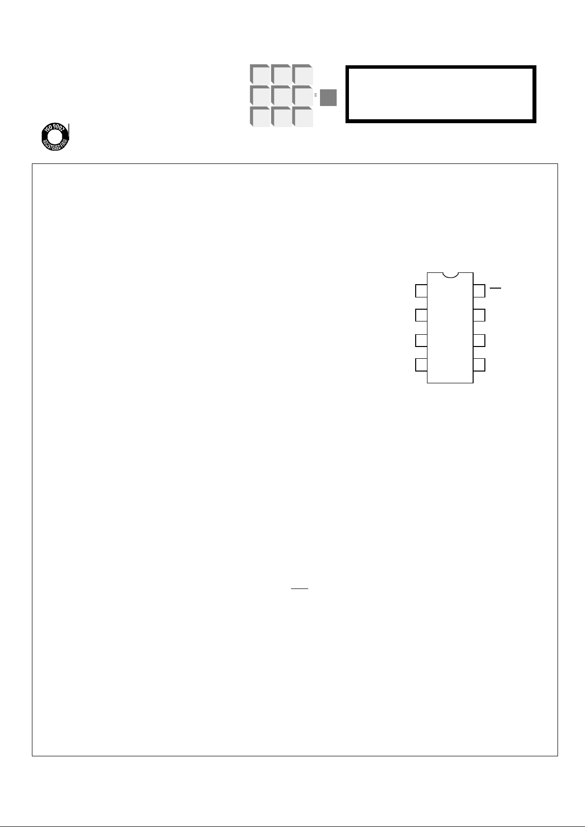
• LS7538, LS7539 (DIP); LS7538-S, LS7539-S (SOIC) - See Figure 1
APPLICATIONS:
• Screw-in and built-in adapter modules for converting table and floor lamps
to touch control for step dimming.
• On-Off touch control of under-cabinet fluorescent lamps (LS7539 only).
DESCRIPTION:
The LS7538 and LS7539 are CMOS integrated circuits which provide trigger pulses for triac phase control of incandescent lamps.
The circuits are designed to operate with a wide variety of lamp sizes ranging from small table lamps to large floor lamps.
The AGC Loop automatically adjusts Touch Sensitivity to be independent of lamp size.
There are 3 different Brightness Step Sequences for each version of the IC which can be selected by the Three-State
MODE pin as shown in Table 1.
TABLE 1. BRIGHTNESS STEP MODES
MODE PIN BRIGHTNESS STEP SEQUENCE
FLOAT OFF-NIGHT LIGHT-MEDIUM-MAXIMUM-OFF
VDD OFF-NIGHT LIGHT- LOW MEDIUM-HIGH MEDIUM-MAXIMUM-OFF
Vss (LS7538) OFF-MAXIMUM-MEDIUM-NIGHT LIGHT-OFF
(LS7539) OFF-MAXIMUM-OFF
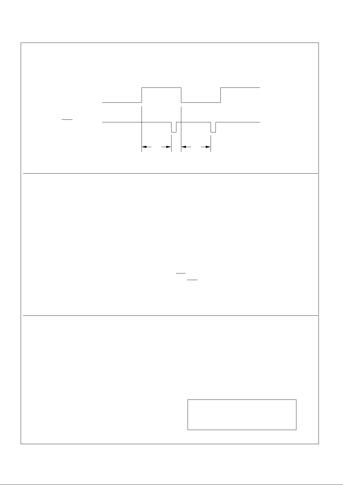
The lamp brightness is made to vary by changing the delay of the TRIG pulse to the triac from the zero-crossing of the
SYNC input. The delays are shown in Table 2 for 50Hz and 60Hz operation along with Delivered Power as a percentage
of Full Power. Figure 2 illustrates the delay.
PIN ASSIGNMENT
TOP VIEW
LSI
1
2
3
4
8
7
6
5
LS7538/7539
FIGURE 1
TRIG
VDD(+V )
MODE
CONTROL
VSS(-V)
SYNC
CLOCK
TOUCH
December 2002
7538/39-120202-1
TABLE 2. BRIGHTNESS POWER LEVELS
Brightness 60Hz Delay (1) 50Hz Delay (2) % PWR (3)
Night Light 6.0 ms 7.2 ms 12
Low Medium 4.8 ms 5.7 ms 35
Medium 4.0 ms 4.8 ms 53
High Medium 3.2 ms 3.8 ms 72
Maximum 0.85 ms 1.0 ms 99
(1) With 300kΩ connected between Pin 1 and VDD. (2) With 360kΩ connected between Pin 1 and VDD.
(3) Percentage of Full Power delivered to a resistive load by the Triac Switch.
LSI/CSI
LSI Computer Systems, Inc. 1235 Walt Whitman Road, Melville, NY 11747 (631) 271-0400 FAX (631) 271-0405
LS7538-LS7539
U
L
®
A3800

INPUT/OUTPUT DESCRIPTION:
CLOCK Input (Pin 1)
An external resistor connected between this input and
VDD, along with an internal capacitor and oscillator stage,
generates a clock which is used for all timing functions.
The recommended value of this resistor for 50Hz and
60Hz operation is specified in the ELECTRICAL CHARACTERISTICS. The resistor value determines the Brightness Levels produced. (See Table 2)
SYNC Input (Pin 2)
50 or 60Hz AC input for zero crossing detection.
VDD (Pin 3)
Supply voltage positive terminal.
TOUCH Input (Pin 4)
Input for sensing that a touch has been made on a lamp
surface or other touch plate.
CONTROL I/O (Pin 5)
An external R-C network connected between this pin
and VDD establishes the controlling feedback for the
AGC Loop.
MODE Input (Pin 6)
A three-state input used to select the desired Brightness Step Sequence (See Table 1). The MODE Input
may be changed during operation.
VSS (Pin 7)
Supply voltage negative terminal.
TRIG (Pin 8)
The TRIG output produces a negative going pulse every half-cycle of the SYNC input to trigger the triac. The
delay, Td, of the pulse with respect to the SYNC signal
determines the Brightness Level produced.
(See Table 2 & Figure 2)
SYNC (Pin 2)
FIGURE 2. OUTPUT DELAY (Td)
Td
Td
TRIG(Pin 8)
ABSOLUTE MAXIMUM RATINGS:
PARAMETER SYMBOL VALUE UNIT
DC supply voltage VDD - VSS +11 V
Any input voltage VIN VSS - 0.5 to VDD + 0.5 V
Operating temperature TA -20 to +85 °C
Storage temperature TSTG -65 to +150 °C
The information included herein is believed to be
accurate and reliable. However, LSI Computer Systems,
Inc. assumes no responsibilities for inaccuracies, nor for
any infringements of patent rights of others which may
result from its use.
7538/39-041597-2
 Loading...