QUADRATURE CLOCK CONVERTER
FEATURES:
• x1, x2 and x4 resolution
• Programmable output pulse width (200ns to 140µs)
• Excellent regulation of output pulse width
• TTL and low voltage CMOS compatible I/Os
• +3V to +5.5V operation (VDD-VSS)
• LS7183, LS7184 (DIP)
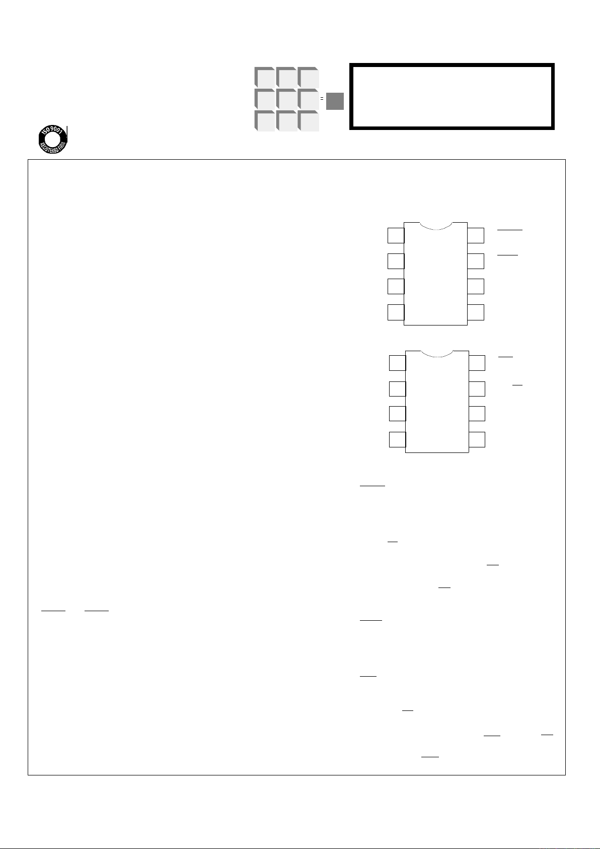
LS7183-S, LS7184-S (SOIC) - See Figure 1
INPUT/OUTPUT DESCRIPTION:
RBIAS (Pin 1)
Input for external component connection. A resistor connected
between this input and VSS adjusts the output clock pulse
width (Tow).
VDD (Pin 2)
Supply Voltage positive terminal.
VSS (Pin 3)
Supply Voltage negative terminal.
A, B (Pin 4, Pin 5)
Quadrature Clock inputs A and B. Directional output pulses are
generated from the A and B clocks according to Fig. 2. A and B
inputs have built-in immunity for noise signals less than 50ns
duration (Validation delay, TVD). The A and B inputs are inhibited during the occurrence of a directional output clock
(UPCK or DNCK), so that spurious clocks resulting from encoder dither are rejected.
MODE (Pin 6)
MODE is a 3-state input to select resolution x1, x2 or x4. The
input quadrature clock rate is multiplied by factors of 1, 2 and 4
in x1, x2 and x4 mode respectively in producing the output
UP/DN clocks (See Fig. 2). x1, x2 and x4 modes selected by
the MODE input logic levels are as follows:
Mode = 0 : x1 selected
Mode = 1 : x2 selected
Mode = Float : x4 selected
LS7183 - DNCK (Pin 7)
In LS7183, this is the DOWN Clock Output. This output
consists of low-going pulses generated when A input
lags the B input.
LS7184LV - UP/DN (Pin 7)
In LS7184, this is the count direction indication output.
When A input leads the B input, the UP/DN output goes
high indicating that the count direction is UP. When A
input lags the B input, UP/DN output goes low,
indicating that the count direction is DOWN.
LS7183 - UPCK (Pin 8)
In LS7083LV, this is the UP Clock output. This output
consists of low-going pulses generated when A input
leads the B input.
LS7184 - CLK (Pin 8)
In LS7184, this is the combined UP Clock and DOWN
Clock output. The count direction at any instant is
indicated by the UP/DN output (Pin 7).
NOTE: For the LS7184, the timing of CLK and UP/DN
requires that the counter interfacing with LS7184 counts
on the rising edge of the CLK pulses.
DESCRIPTION:
The LS7183 and LS7184 are monolithic CMOS silicon gate
quadrature clock converters. Quadrature clocks derived from
optical or magnetic encoders, when applied to the A and B
inputs of the LS7183/LS7184, are converted to strings of Up
Clocks and Down Clocks (LS7183) or to a Clock and an Up/
Down direction control (LS7184). These outputs can be interfaced directly with standard Up/Down counters for direc-
tion and position sensing of the encoder.
August 2001
RBIAS
VDD(+V)
VSS(-V)
A B
MODE
DNCK
UPCK
PIN ASSIGNMENT - TOP VIEW
CLK
UP/DN
FIGURE 1
1
2
3
4
8
7
6
5
LS7184
RBIAS
VDD(+V)
VSS(-V)
A B
MODE
1
2
3
4
8
7
6
5
LS7183
LSI LSI
7183/84-071201-1
LSI/CSI
LSI Computer Systems, Inc. 1235 Walt Whitman Road, Melville, NY 11747 (631) 271-0400 FAX (631) 271-0405
LS7183/LS7184
U
L
®
A3800

ABSOLUTE MAXIMUM RATINGS:
PARAMETER SYMBOL VALUE UNITS
DC Supply Voltage VDD - VSS 7.0 V
Voltage at any input VIN VSS - .3 to VDD + .3 V
Operating temperature TA -20 to +85 °C
Storage temperature TSTG -55 to +150 °C
7183/84-070601-2
DC ELECTRICAL CHARACTERISTICS:
(Unless otherwise specified VDD = 3V to 5V and TA = -20°C to 85°C)
PARAMETER SYMBOL MIN TYPE MAX UNITS CONDITON
Supply Voltage VDD 3.0 - 5.5 V Supply current IDD - 30 45 µA VDD = 3V
IDD - 110 150 µA VDD = 5V
MODE input:
Logic 0 Vml - - 0.6 V -
Logic 1 Vmh VDD -0.6 - - V Logic float Vmf (VDD/2) - 0.5 VDD/2 (VDD/2) + 0.5 V -
Logic 0 input current Iml - 3.0 5.0 µA VDD = 3V
Iml - 12.0 16.0 µA VDD = 5V
Logic 1 input current Imh - -3.0 -5.0 µA VDD = 3V
Imh - -12.0 -16.0 µA VDD = 5V
A,B inputs:
Logic 0 VABl - - 0.3VDD V Logic 1 VABh 0.7VDD - - V Input current IABlk - 0 10 nA -
RBIAS input:
External resistor RB 5k - 10M ohm -
All outputs:
Sink current Iol -1.2 -1.8 - mA Vo = 0.5V, VDD = 3V
Iol -2.5 -3.5 - mA Vo = 0.5V, VDD = 5V
Source current Ioh 1.2 1.8 - mA Vo = 2.5V, VDD = 3V
Ioh 2.5 3.5 - mA Vo = 4.5V, VDD = 5V
TRANSIENT CHARACTERISTICS
(TA = -20°C to 85°C)
PARAMETER SYMBOL MIN TYPE MAX UNITS CONDITON
Output Clock Pulse Width TOW 190 - - ns See Fig. 2
A,B inputs:
Validation Delay TVD - 25 50 ns VDD = 5V
TVD - 50 100 ns VDD = 3V
Phase Delay TPS TVD +TOW - Infinite s Pulse Width TPW 2TPS - Infinite s Frequency fA,B - - 1/(2TPW) Hz Inupt to Output Delay TDS - 200 270 ns VDD = 3V
TDS - 110 150 ns VDD = 5V
 Loading...