


24-BIT QUADRATURE COUNTER
FEATURES:
• Programmable modes are: Up/Down,
Binary, BCD, 24 Hour Clock, Divide-by-N,
x1 or x2 or x4 Quadrature and Single Cycle.
• DC to 20 MHz Count Frequency.
• 8-Bit I/O Bus for Microprocessor
Communication and Control.
• 24-Bit comparator for pre-set count
comparison.
• Readable status register.
• Input/Output TTL and CMOS compatible.
• 5 Volt operation (Vdd - Vss).
• LS7166 (DIP); LS7166-S (SOIC);
LS7166-TS24 (24-Pin TSSOP)* - See Fig. 1
GENERAL DESCRIPTION:
The LS7166 is a CMOS, 24-bit counter that
can be programmed to operate in several different modes. The operating mode is set up
by writing control words into internal control
registers (see Figure 8). There are three 6-bit
and one 2-bit control registers for setting up
the circuit functional characteristics. In addition to the control registers, there is a 5-bit output status register (OSR) that indicates the current counter status. The IC communicates with
external circuits through an 8-bit three state I/O
bus. Control and data words are written into
the LS7166 through the bus. In addition to the
I/O bus, there are a number of discrete inputs
and outputs to facilitate instantaneous hardware based control functions and instantaneous status indication.
REGISTER DESCRIPTION:
Internal hardware registers are accessible
through the I/O bus (D0 - D7) for READ or
WRITE when CS = 0. The C/D input selects
between the control registers (C/D = 1) and the
data registers (C/D = 0) during a READ or
WRITE operation. (See Table 1)
The information included herein is believed to be
accurate and reliable. However, LSI Computer Systems,
Inc. assumes no responsibilities for inaccuracies, nor for
any infringements of patent rights of others which may
result from its use.
(Write Input) WR
(Chip Select Input) CS
(Load Counter/Load Latch) LCTR/LLTC
(A, B Gate/Reset Counter)ABGT/RCTR
VDD (+5V)
(Count Input) A
(Count Input) B
D0
D1
D2
VSS (GND)
RD (Read Input)
C/D (Control/ Data Input)
BW (Borrow Output)
CY (Carry Output)
D7
D6
D5
D4
D3
1
2
3
4
5
6
7
8
9
10
11
12
13
14
15
16
17
18
19
20
LSI
LS7166
December 2002
FIGURE 1
7166-120902-1
LSI/CSI
LSI Computer Systems, Inc. 1235 Walt Whitman Road, Melville, NY 11747 (631) 271-0400 FAX (631) 271-0405
LS7166
U
L
®
A3800
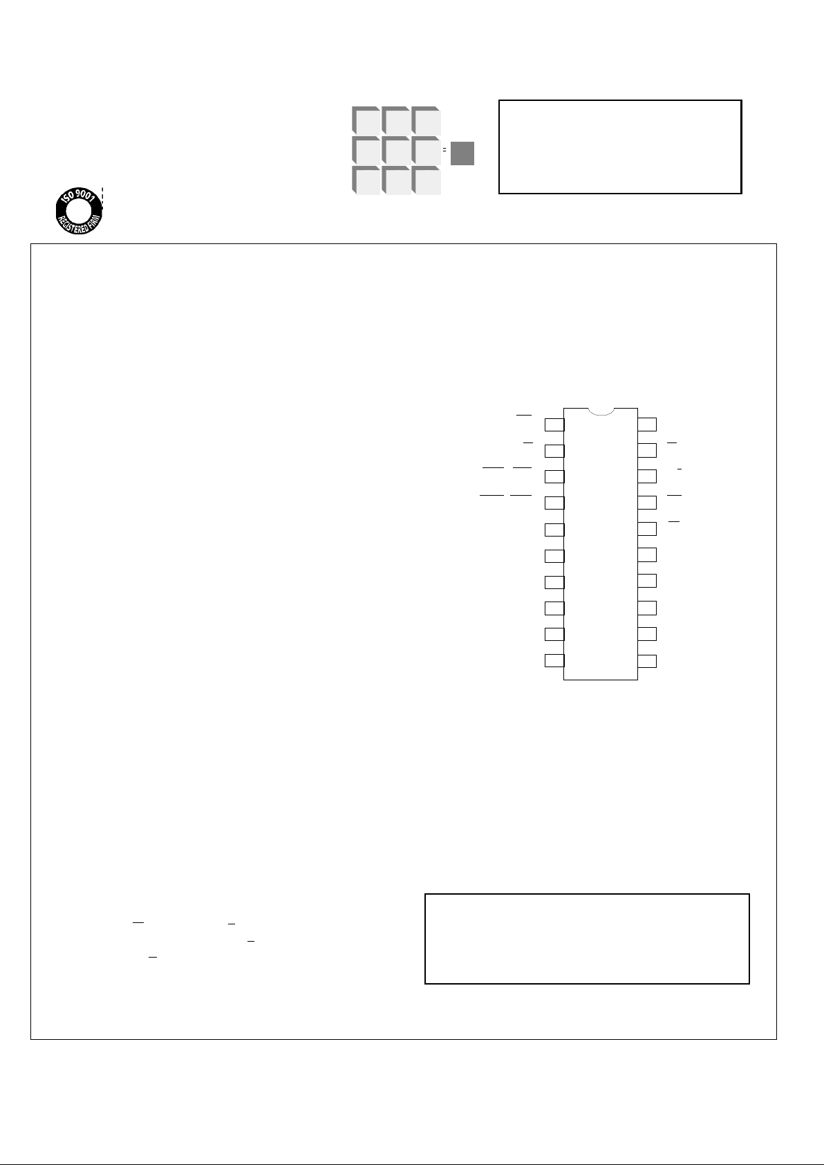
20-Pin Package PIN ASSIGNMENT - Top View
*(Contact factory for 24-Pin TSSOP Package Pinout)
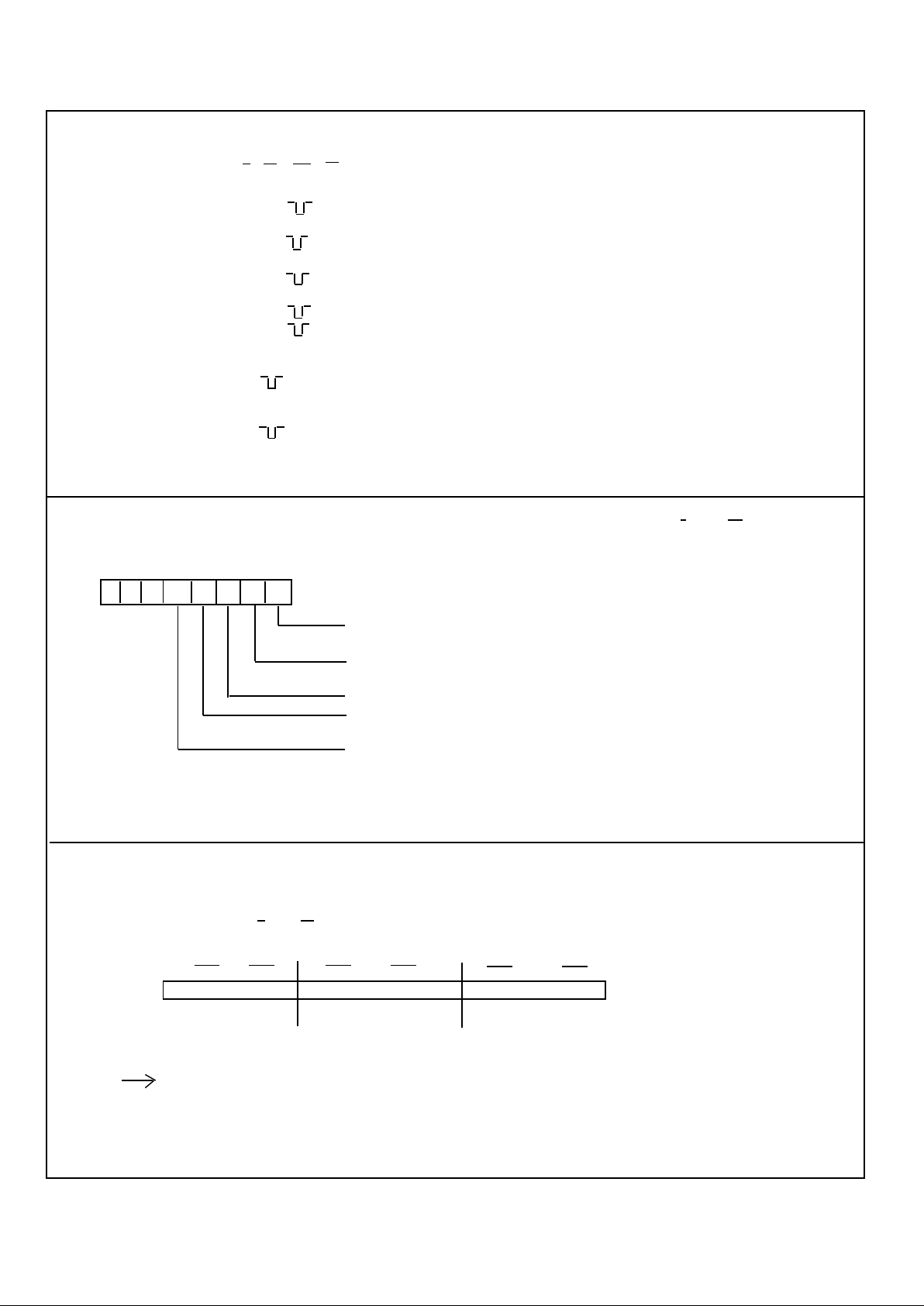
OSR (Output Status Register). Indicates CNTR status: Accessed by: READ when C/D = 1, CS = 0.
Bit # 7 6 5 4 3 2 1 0
U U U 0/1 0/1 0/1 0/1 0/1
BWT. Borrow Toggle Flip-Flop. Toggles everytime CNTR underflows
generating a borrow.
CYT. Carry Toggle Flip-Flop. Toggles everytime CNTR overflows
generating a carry.
COMPT. Compare Toggle Flip-Flop. Toggles everytime CNTR equals PR
SIGN. Sign bit. Reset ( = 0) when CNTR underflows
Set ( = 1) when CNTR overflows
UP/DOWN. Count direction indicatior in quadrature mode.
Reset ( = 0) when counting down
Set ( = 1) when counting up
(Forced to 1 in non-quadrature mode)
OL(Output latch). The OL is the output port for the CNTR. The 24 bit CNTR Value at any instant can be accessed
by performing a CNTR to OL transfer and then reading the OL in 3 READ cycle sequence of Byte 0 (OL0), Byte 1 (OL1)
and Byte 2 (OL2). The address pointer for OL0/OL1/OL2 is automatically incremented with each READ cycle.
Accessed by: READ when C/D = 0, CS = 0.
Bit # 7 0 7 0 7 0
OL2 OL1 OL0
(BYTE 2) (BYTE 1) (BYTE 0)
Standard Sequence for Loading and Reading OL:
3 MCR ; Reset OL address pointer and Transfer CNTR to OL
READ OL ; Read Byte 0 and increment address
READ OL ; Read Byte 1 and increment address
READ OL ; Read Byte 2 and increment address
TABLE 1 - Register Addressing Modes
D7 D6 C/D RD WR CS COMMENT
X X X X X 1 Disable Chip for READ/WRITE
0 0 1 1 0 Write to Master Control Register (MCR)
0 1 1 1 0 Write to input control register (ICR)
1 0 1 1 0 Write to output/counter control register (OCCR)
1 1 1 1 0 Write to quadrature register (QR)
X X 0 1 0 Write to preset register (PR) and increment register
address counter.
X X 0 1 0 Read output latch (OL) and increment register
address counter
X X 1 1 0 Read output status register (OSR).
X = Don't Care
U = Undefined
7166-062394-3
PR (Preset register). The PR is the input port for the CNTR. The CNTR is loaded with a 24 bit data via the PR. The
data is first written into the PR in 3 WRITE cycle sequence of Byte 0 (PR0), Byte 1 (PR1) and Byte 2 (PR2).
The address pointer for PR0/PR1/PR2 is automatically incremented with each write cycle.
Accessed by: WRITE when C/D = 0, CS = 0.
Bit # 7 - - - - - - - - - - 0 7 - - - - - - - - - - 0 7 - - - - - - - - - - 0
PR2 PR1 PR0
(BYTE 2) (BYTE 1) (BYTE 0)
Standard Sequence for Loading PR and Reading CNTR:
1 MCR ; Reset PR address pointer
WRITE PR ; Load Byte 0 and into PR0 increment address
WRITE PR ; Load Byte 1 and into PR1 increment address
WRITE PR ; Load Byte 2 and into PR3 increment address
8 MCR ; Transfer PR to CNTR
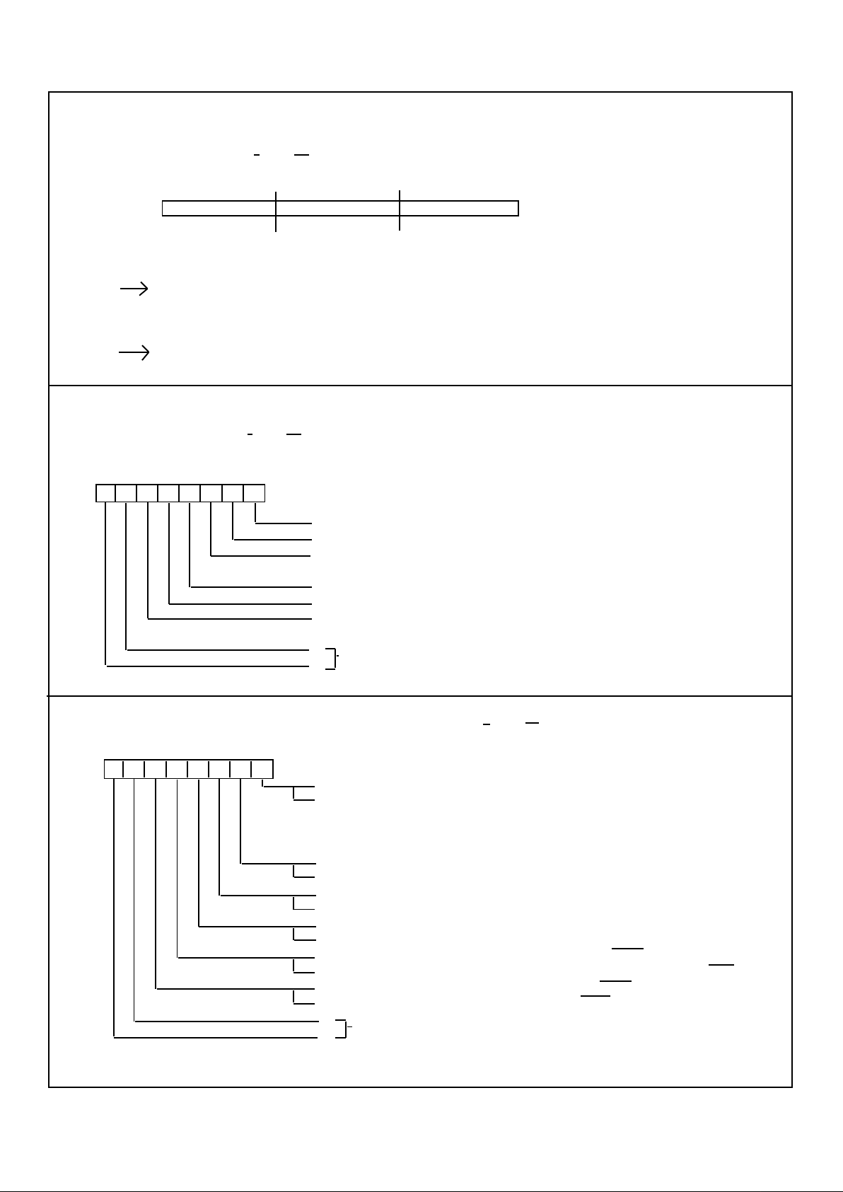
MCR (Master Control Register). Performs register reset and load operations. Writing a "non-zero” word to MCR does
not require a follow-up write of an “all-zero” word to terminate a designated operation.
Accessed by: WRITE when C/D = 1, CS = 0.
Bit # 7 6 5 4 3 2 1 0
0 0
1: Reset PR/OL address pointer
1: Transfer CNTR to OL (24 bits)
1: Reset CNTR, BWT and CYT. Set SIGN bit.
(CNTR=0, BWT=0, CYT=0, SIGN=1)
1: Transfer PR to CNTR (24 bits)
1: Reset COMPT (COMPT = 0)
1: Master reset. Reset CNTR, ICR, OCCR, QR, BWT, CYT, OL
COMPT, and PR/OL address pointer. Set PR (PR=FFFFFF) and SIGN.
0: Select MCR
0:
NOTE: Control functions may be combined.
ICR (Input Control Register). Initializes counter input operating modes.
Accessed by: WRITE when C/D = 1, CS = 0.
Bit # 7 6 5 4 3 2 1 0
0 1
0: Input A = Up count input, Input B = Down count input
1: Input A = Count input, Input B = Count direction input (overridden in
quadrature mode) where B = 0 selects up count mode and B =1
selects Down count mode.
(NOTE: During counting operation B may switch only when A = 1.)
0: NOP
1: Increment CNTR once (A/B = 1, if enabled)
0: NOP
1: Decrement CNTR once (A/B = 1, if enabled)
0: Disable inputs A/B
1: Enable inputs A/B
0: Initialize Pin 4 as CNTR Reset input (Pin 4 = RCTR)
1: Initialize Pin 4 as Enable/Disable gate for A/B inputs (Pin 4 = ABGT)
0: Initialize Pin 3 as CNTR load input (Pin 3 = LCTR)
1: Initialize Pin 3 as OL load input (Pin 3 = LLTC)
1: Select ICR
0:
NOTE: Control functions may be combined.
7166-062394-2
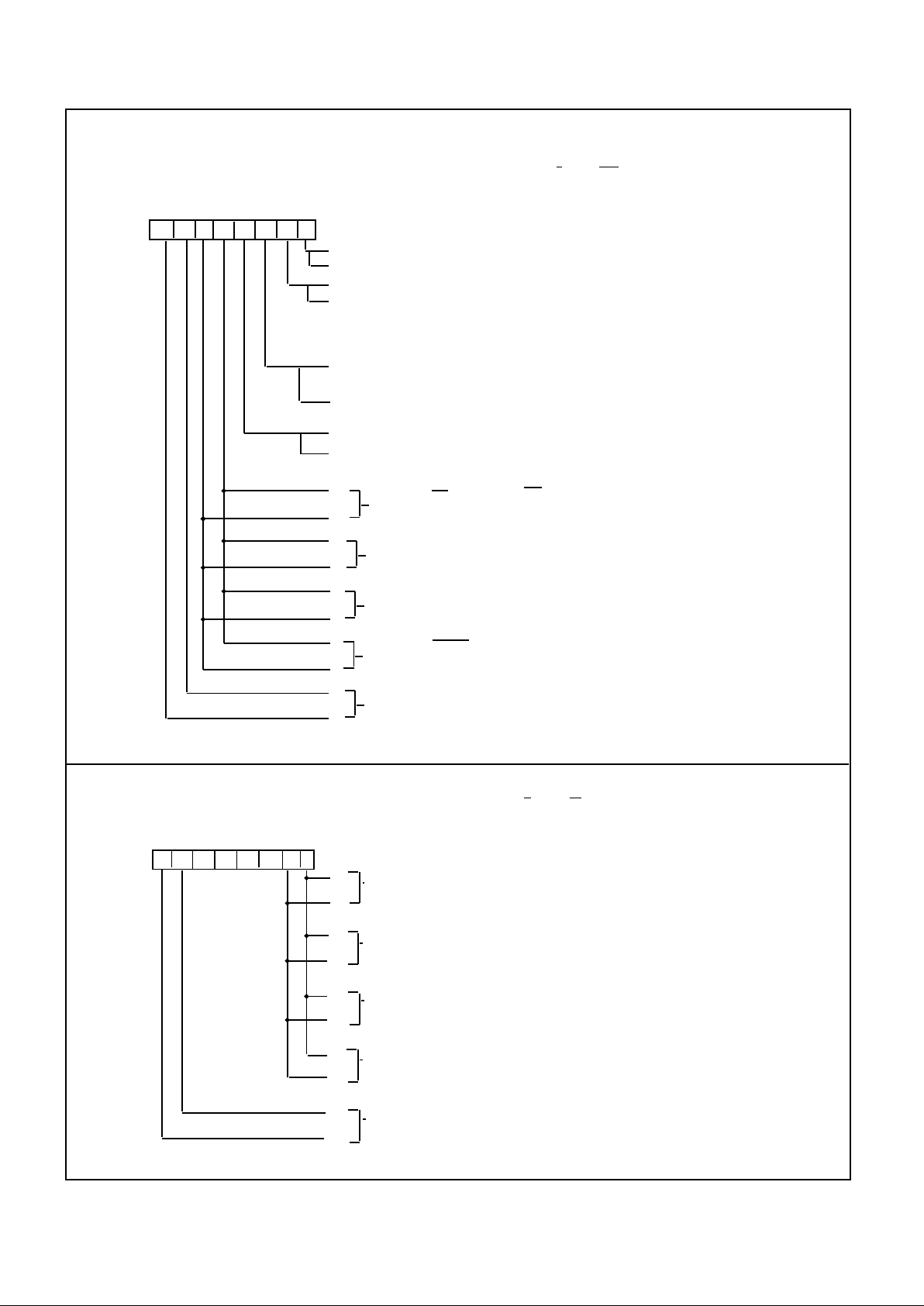
OCCR (Output Control Register) Initializes CNTR and output operating modes.
Accessed by : WRITE when C/D = 1, CS = 0.
Bit # 7 6 5 4 3 2 1 0
1 0
0: Binary count mode (Overridden by D3 = 1).
1: BCD count mode (Overridden by D3 = 1)
0: Normal count mode
1: Non-Recycle count mode. (CNTR enabled with a Load or Reset
CNTR and disabled with generation of Carry or Borrow.
In this mode no external CY or BW is generated. Instead
CYT or BWT should be used as cycle completion indicator.)
0: Normal count mode
1: Divide by N count mode (CNTR is reloaded with PR data upon
Carry or Borrow).
0: Binary or BCD count mode (see D0)
1: 24 Hour Clock mode with Byte 0 = Sec, Byte 1 = Min and Byte 2 = Hr.
(Overrides BCD/Binary Modes)
0
Pin 16 = CY, Pin 17 = BW. (Active Low)
0
1
Pin 16 = CYT, Pin 17 = BWT
0
0
Pin 16 = CY, Pin 17 = BW. (Active high)
1
1
Pin 16 = COMP, Pin 17 = COMPT
1
0
Select OCCR
1
QR (Quadrature Register). Selects quadrature count mode (See Fig. 7)
Accessed by: WRITE when C/D = 1, CS = 0.
Bit # 7 6 5 4 3 2 1 0
1 1 X X X X
0
Disable quadrature mode
0
1
Enable x1 quadrature mode
0
0
Enable x2 quadrature mode
1
1
Enable x4 quadrature mode
1
1
Select QR
1
7166-062394-4
X = Don’t Care