

DIGITAL FILTER RC
LSI/CSI
LS6511
U
A3800
LSI Computer Systems, Inc. 1235 Walt Whitman Road, Melville, NY 11747 (631) 271-0400 FAX (631) 271-0405
®
L
PIR MOTION DETECTOR
FEATURES:
• Direct Interface with PIR Sensor
• Two-Stage Differential Amplifier
• Amplifier Gain and Bandwidth externally controlled
• True and Complementary Output Drives
• Separate digital filters for processing positive and
negative input signals
• Single Pulse/Dual Pulse/ Concurrent Pulse Detection
• Adjustable Output Pulse Width
• Optional 5V Shunt Regulator Output
• 50 µA Typical Supply Current
• Undervoltage Detection
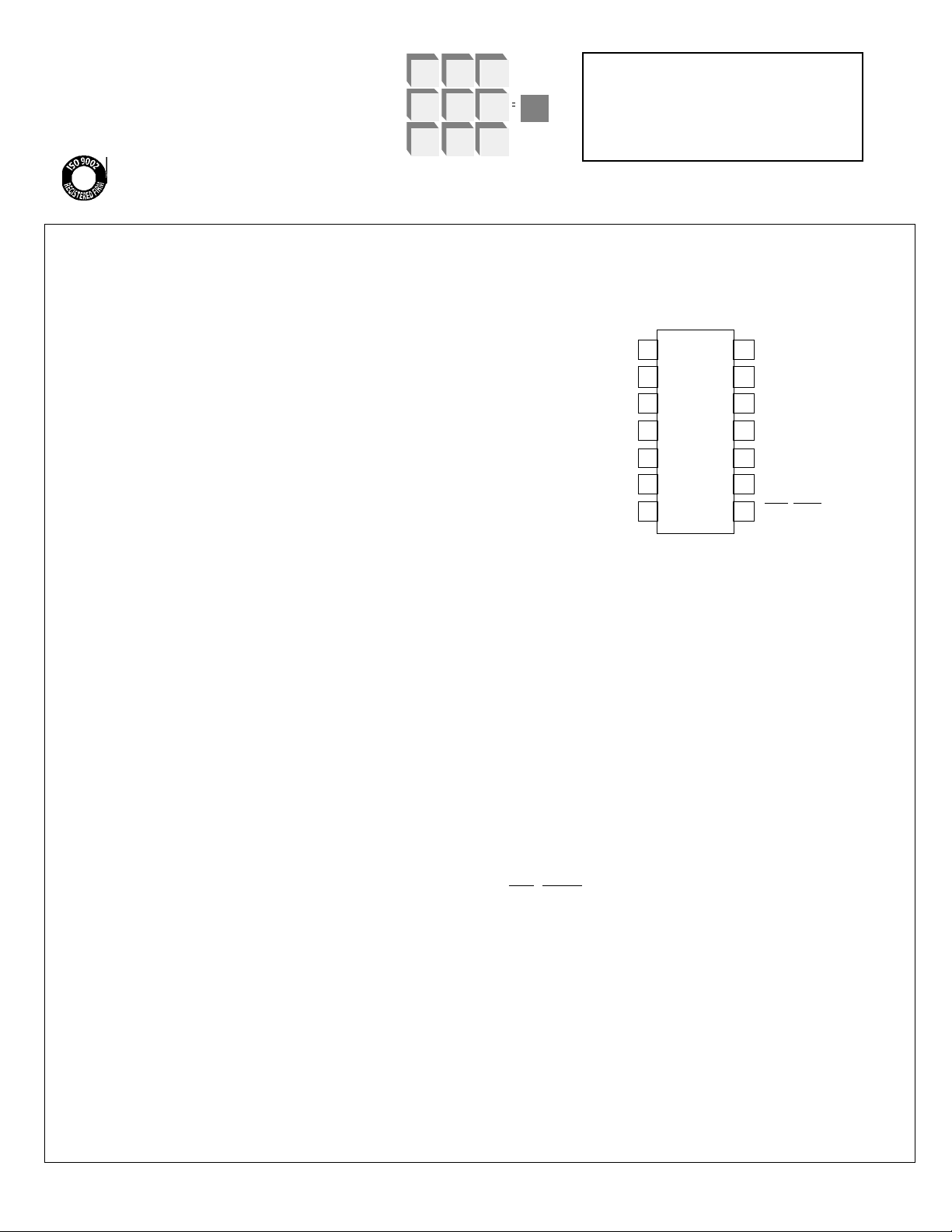
• 14-Pin DIP or 14-Pin SOIC - See Figure 1
DESCRIPTION:
The LS6511 is a CMOS Silicon Gate integrated circuit, designed
for detecting motion from a PIR Sensor and initiating appropriate
responses. Referring to Figure 2, the detailed description of the
functional blocks are as follows:
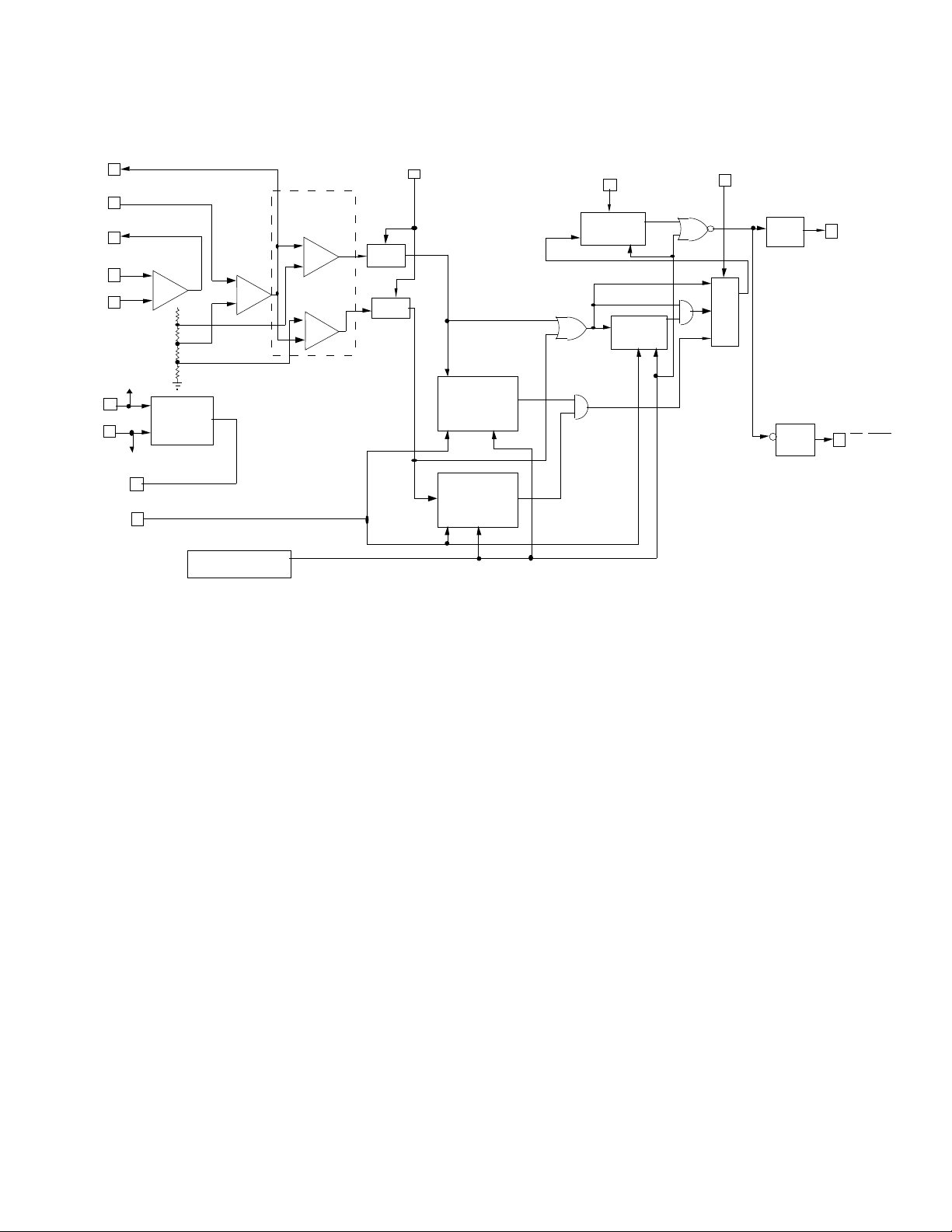
DIFFERENTIAL AMPLIFIER
Each stage of the two stage Differential Amplifier can be set to
have its own amplification and bandwidth. The two inputs to the
first stage allow for single-ended or differential connection to PIR
Sensors. This stage can be biased anywhere in its dynamic
range. The second stage is internally biased so that the Window
Comparator’s lower and higher thresholds can be fixed relative to
this bias. Signal levels as low as 100µV can be detected.
WINDOW COMPARATOR
The Window Comparator provides noise filtering by enabling only
those signals equal to or greater than a fixed threshold at the output of the Differential Amplifier to appear at the 2 outputs of the
Window Comparator. One output detects positive input signals
while the other output detects negative input signals.
April 2000
PIN ASSIGNMENT - TOP VIEW
DIFF. AMP. 1 OUTPUT
DIFF. AMP. 2 INPUT (-)
DIFF. AMP. 2 OUTPUT
ONE-SHOT/WINDOW TIMER RC
DURATION TIMER RC LED/RELAY OUTPUT
MODE SELECT
PROGRAMMABLE RETRIGGERABLE ONE-SHOTS
Positive and negative input signals at the digital filter outputs will
generate retriggerable one-shot pulses. In the Concurrent Pulse
Mode, outputs from each one-shot must occur together at some
point in time to cause an output to occur. The one-shot pulse
width is programmable using an external RC network. Typical
pulse widths used vary between 1 and 12 seconds.
WINDOW TIMER
In the Dual Pulse Mode any two detections must occur within a
timing window to cause an output to occur. The timing window is
programmable using an external RC network. Typical windows
are between 1 and 5 seconds.
OUTPUT DURATION TIMER
The duration timer is retriggerable and programmable using an
external RC network. Typical duration times are between 0.5 and
15 seconds. Successive input detections will restart the timer.
1
2
3
4
5
6
7
LSI
LS6511
FIGURE 1
DIFF. AMP 1 INPUT (-)
14
DIFF. AMP 1 INPUT (+)
13
5V REGULATOR OUTPUT
12
VDD
11
10
9
8
(+V)
VSS
(-V)
LED/RELAY OUTPUT
COMPARATOR DIGITAL FILTER
The outputs of the Window Comparator are filtered so that motion must be present for a certain duration before it can be recognized and appear as pulses at the Digital Filter outputs. An external RC network sets the duration time. Nominal duration is
50ms.
MODE SELECT
A tristate input pin selects how the detected signals are processed. When the input is a logic 0, detection from either a positive or negative input signal at the Digital Filter outputs will cause
an LED/RELAY output to occur (Single Pulse Mode). When the
input is floating, detection from a positive and negative input signal must occur within a specific time before an output will occur
(Concurrent Pulse Mode). When the input is a logic 1, any two
detections within a specific time will cause an output to occur
(Dual Pulse Mode).
6511-040400-1
OUTPUTS
The LED/RELAY Output is an open drain output that will sink current when an input signal is detected and processed and when
the Power Supply drops below 3.7V (Typical) (Undervoltage Detection). The Undervoltage Detection will be removed when the
Power Supply rises above 3.9V (Typical). The LED/RELAY Output performs identically but is opposite in polarity. The output can
sink current from a relay coil returned to a positive voltage (VDD
to 9.5V maximum).
SHUNT REGULATOR
The LS6511 includes a 5V Shunt Regulator Output which can be
tied to the VDD Pin so that the circuit can be powered from a
higher voltage power supply.
DIFF AMP 2
5
OUTPUT
DIFF AMP 2
INPUT (-)
DIFF AMP 1
OUTPUT
DIFF AMP 1
INPUT (-)
DIFF AMP 1
INPUT (+)
3
2
1
14
13
-
AMP
+
VDD
-
AMP
+
WINDOW
COMPARATOR
+
COMP
-
+
COMP
-
DIGITAL FILTER RC
4
DIGITAL
FILTER
DIGITAL
FILTER
DURATION
TIMER RC
6
OUTPUT
DURATION
TIMER
WINDOW
TIMER
MODE
SELECT
7
M
U
X
DRIVER
9
LED/RELAY
OUTPUT
VDD
11
VSS
10
5 V REGULATOR
OUTPUT
ONE-SHOT/
WINDOW TIMER RC
(+V)
(-V)
12
SHUNT
REGULATOR
UNDERVOLTAGE
DETECTOR
PROGRAMMABLE
RETRIGGERABLE
ONE-SHOT
PROGRAMMABLE
RETRIGGERABLE
ONE-SHOT
FIGURE 2. LS6511 BLOCK DIAGRAM
DRIVER
LED/RELAY
8
OUTPUT
ABSOLUTE MAXIMUM RATINGS:
PARAMETER SYMBOL VALUE UNIT
DC supply voltage VDD-VSS +7 V
Any input voltage VIN VSS-0.3 to VDD + 0.3 V
Operating temperature TA -40 to +85 °C
Storage temperature TSTG -65 to +150 °C
ELECTRICAL CHARACTERISTICS:
( All voltages referenced to VSS, TA = -40˚C to +55˚C, 4.5V≤ VDD ≤6.5V, unless otherwise specified.)
PARAMETER SYMBOL MIN TYP MAX UNIT CONDITIONS
SUPPLY CURRENT:
VDD = 5V IDD - 50 75 µA LED/RELAY, LED/RELAY
VDD = 4.5V-6.5V IDD - 65 125 µA and REGULATOR
outputs not loaded
REGULATOR:
Voltage VR 5.00 5.75 6.25 V -
Current IR - - 10 mA -
DIFFERENTIAL AMPLIFIERS:
Open Loop Gain, Each Stage G 70 - - dB -
Common Mode Rejection Ratio CMRR 60 - - dB -
Power Supply Rejection Ratio PSRR 60 - - dB -
Input Sensitivity VS 100 - - µVp-p TA = 25˚C, with Amplifier
(Minimum Detectable Voltage Bandpass configuration
to first amplifier when both as shown in Figure 3
amplifiers are cascaded for
a net gain of 8,000)
Input Dynamic Range - 0 - 1.75 V -
Diff. Amp 2 Internal VIR - 0.3VDD - V -
Reference
COMPARATOR:
Lower Reference VTHL - VIR-0.8V - V At VDD = 5.75V
Higher Reference VTHH - VIR+0.8V - V At VDD = 5.75V
DIGITAL FILTER:
For 50ms Filter Time RDF - 2.2 - MΩ -
CDF - 0.01 - µF -
ONE SHOT ROS - 2.2 - MΩ -
(1 Second) COS - 0.22 - µF -
WINDOW TIMER RWT - 2.2 - MΩ -
(2.5 Second) CWT - 0.68 - µF -
DURATION TIMER RDT - 2.2 - MΩ (5 Seconds) CDT - 0.68 - µF -
OUTPUT DRIVE CURRENT IO -20 - - mA VDD = 5V
(Vo = 0.5V Max.)
6511-022900-2
The information included herein is believed to be
accurate and reliable. However, LSI Computer Systems,
Inc. assumes no responsibilities for inaccuracies, nor for
any infringements of patent rights of others which may
result from its use.
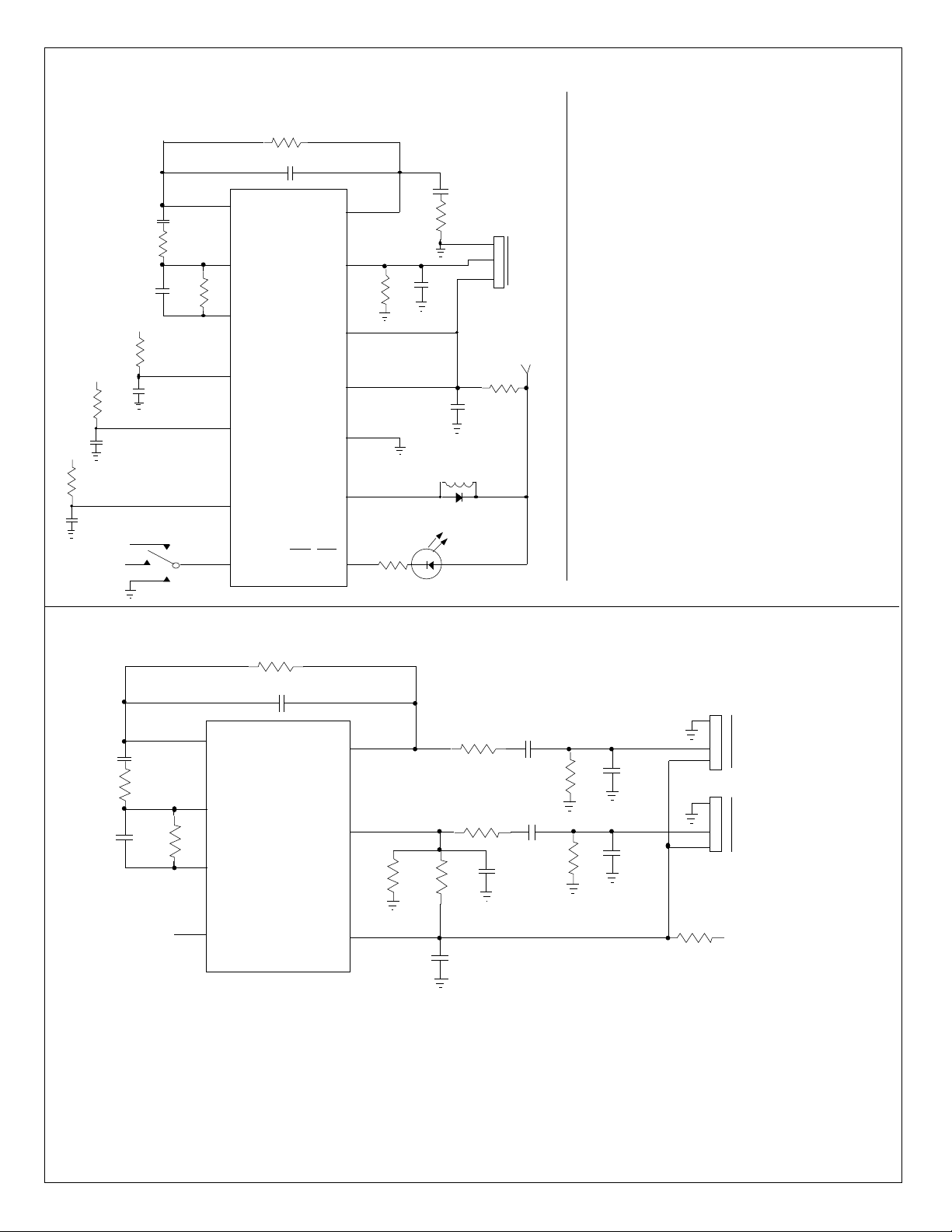
FIGURE 3. TYPICAL RELAY APPLICATION
DD
OUT
(+)IN
NOTE 1: The relay coil is normally energized and the LED is off. When an alarm
occurs, the relay coil becomes de-energized and the LED is turned on.
R3
C3
+
LED
C9
C1
RELAY
COIL
C2
R2
PIR
SENSOR
RAW
DC
INPUT
R1
+
-
VDD
C8
VDD
R8
R7
C7
VDD
R6
C6
1
2
R5
3
4
5
AMP 1
OUT
AMP 2
(-)IN
AMP 2
OUT
DIG FILTER
RC
OS/WT
RC
C4
+
R4
C5
AMP 1
AMP 1
5V REG
(-)IN
(+)IN
OUT
VDD
VSS
14
13
R9
12
11
10
LS6511
DUR TIM
RC
MODE
LED/REL
LED/REL
6
V
7
OUT
9
R10
8
R1 = See NOTE 2
R2 = 36KΩ
R3 = 2.7MΩ
R4 = 36KΩ
R5 = 2.7MΩ
R6 = 2.2MΩ (Typical)
R7 = 2.2MΩ (Typical)
R8 = 2.2MΩ (Typical)
R9 = 24KΩ
R10 = 5.1KΩ (Typical)
C1 = 100µF
C2 = 33µF
C3 = 0.01µF
C4 = 33µF
C5 = 0.01µF
C6 = 0.01µF (Typical)
C7 = 0.22µF(O.S. MODE) (Typical)
C7 = 0.68µF(W.T. MODE) (Typical)
C8 = 0.01µF (Typical)
C9 = 0.1µF
D1 = 1N4001
RELAY = No typical P/N
PIR = HEIMANN LHi 954, 958, 978,
874 or 878 (Typical)
All Resistors 1/4W All Capacitors 10V
NOTE 2: R1 is selected to provide sufficient
current to drive the LS6511 and PIR Sensor. Any
surplus current is available to drive additional
D1
loads applied to the 5V Shunt Regulator output or
is absorbed by the 5V Shunt Regulator. Refer to
specifications for current limits.
FIGURE 4. DIFFERENTIAL INTERFACE TO PIR SENSOR PAIR
R2
C2
C7
C5
+ -
C6
+ -
R7
R8
C8
C9
R1
1
C3
+
AMP 1
OUT
AMP 1
(-)IN
14
R5
R3
2
C4
R4
3
12
AMP 2
(-)IN
AMP 2
OUT
5V REG
OUT
AMP 1
LS6511
13
R10
VDD
R9
+
-
R6
C1
R1 = 1KΩ R6 = 36KΩ C1 = 100µF C6 = 33µF
R2 = 2.7MΩ R7 = 36KΩ C2 = 0.01µF C7 = 0.01µF
R3 = 36KΩ R8 = 36KΩ C3 = 33µF C8 = 0.1µF
R4 = 2.7MΩ R9 = 5.6MΩ C4 = 0.01µF C9 = 0.1µF
R5 = 36KΩ R10 = 2.4MΩ C5 = 33µF
PIRs = HEIMANN LHi 954, 958, 978, 874 or 878 (Typical)
PIR
SENSOR 1
PIR
SENSOR 2
5V
6511-040600-4
All Resistors 1/4 W. All Capacitors 10V
NOTES: 1) A pair of PIR Sensors may be used in applications where a wider optical field of view is needed.
2) External 5V Regulator drives the LS6511 and PIR sensor.
 Loading...