

LSI/CSI
LS6501LP
U
A3800
LSI Computer Systems, Inc. 1235 Walt Whitman Road, Melville, NY 11747 (631) 271-0400 FAX (631) 271-0405
L
®
PIR MOTION DETECTOR
FEATURES:
• Low Quiescent Current
• Direct Interface with PIR Sensor
• Two-Stage Differential Amplifier
• Amplifier Gain and Bandwidth externally controlled
• Window Comparator and Digital Filter limit Noise
• Triac or Relay Output Drive
• Programmable Output Duration Timer
• Ambient Light Level Inhibit input
• Selectable Dead Time
• Single or Dual Pulse Detection
• Timing derived from RC Oscillator or 50Hz/60Hz AC
• Regulated 5V Output for PIR Sensor
• Motion Detection LED Indicator
• Triac can drive Incandescent or Fluorescent Lamps
• LS6501LP (DIP), LS6501LP-S (SOIC-NB)
LS6501LP-SW (SOIC-WB) - See Figure 1
APPLICATIONS:
• Automatic Light Control
• Intrusion Alarm
DESCRIPTION: (See Figure 2)
The LS6501LP is a monolithic, CMOS Silicon Gate integrated circuit, designed for detecting motion from a PIR
Sensor and initiating appropriate responses. The detailed
description of the functional blocks is as follows:
DIFFERENTIAL AMPLIFIER
Each stage of the two stage Differential Amplifier can be set
to have its own amplification and bandwidth. The two inputs
to the first stage allow for single ended or differential connection to PIR Sensors. This stage can be biased anywhere
in its dynamic range. The second stage is internally biased
so that the Window Comparator’s lower and higher thresholds can be fixed relative to this bias.
WINDOW COMPARATOR
The Window Comparator provides noise filtering by enabling
only those signals equal to or greater than a fixed threshold
at the output of the Differential Amplifier to appear at the
output of the Window Comparator.
COMPARATOR DIGITAL FILTER
The output of the Window Comparator is filtered so that
motion must be present for a certain duration before it can
be recognized and appear as pulses at the Digital Filter
output.
6501LP-071201-1
July 2001
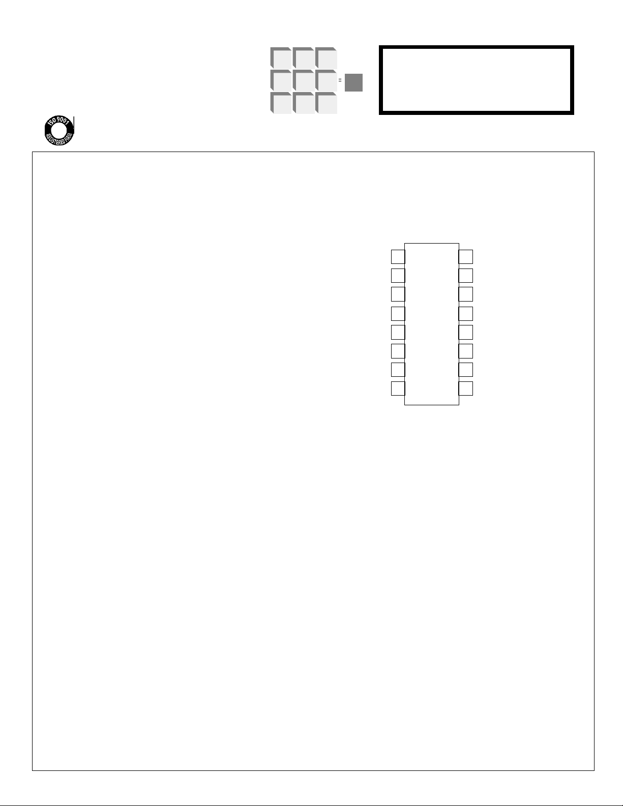
PIN ASSIGNMENT - TOP VIEW
DIFF. AMP. 1 OUTPUT
DIFF. AMP. 2 INPUT (-)
DIFF. AMP. 2 OUTPUT
OSCILLATOR INPUT
AC INPUT
VSS
TRIAC/RELAY OUTPUT
VDD
LSI
1
2
3
LS6501LP
4
5
6
7
8
FIGURE 1
16
DIFF. AMP 1 INPUT (-)
15
DIFF. AMP 1 INPUT (+)
14
5V REGULATOR OUTPUT
13
TIMER CONTROL INPUT
12
DEAD TIME SELECT INPUT
11
INHIBIT INPUT
PULSE MODE
10
SELECT INPUT
9
LED OUTPUT
OUTPUT DURATION TIMER
The voltage level at the TIMER CONTROL input can
select 16 different timeouts for this Timer (See Table 1).
The selection can be made by varying the setting of a
potentiometer. The Timer is retriggerable and controls
the ON duration of the TRIAC/RELAY output. The trigger
for the Timer is generated from pulses appearing at the
Digital Filter output.
SINGLE PULSE/DUAL PULSE MODES
A Single Pulse or Dual Pulse (two pulses occurring within
a specified time period) at the Digital Filter output can be
selected as the trigger for the Output Duration Timer.
This selection is made by the logic level at the PULSE
MODE SELECT input. Logic 0 = Single Pulse Mode,
logic 1 = Dual Pulse Mode.
LED OUTPUT
This is an open drain output which is turned on by pulses
generated by a retriggerable one-shot. The one-shot is
triggered by the leading edge of pulses appearing at the
Digital Filter output. When turned on, this output can sink
current from a series Resistor-LED network returned to a
positive voltage (VDD to 12.5V maximum). This results in
the LED lighting whenever motion is detected.

INHIBIT
The Output Duration Timer can be inhibited from triggering by the voltage level at the INHIBIT input. When this
voltage level exceeds the Inhibit Threshold, the Timer will
be prevented from triggering if it is OFF. If the Timer is
ON, the INHIBIT input is blocked from affecting the Timer.
There is approximately 10% hysteresis between the Inhibit and Enable thresholds at the INHIBIT input. The LED
output is not affected by the INHIBIT input. An adjustable
Ambient Light Level Inhibit can be implemented by connecting a Light Determining Resistor (LDR) network to the
INHIBIT input (See Figures 3 and 4).
DEAD TIME
False turn-ons are prevented from occurring by establishing a Dead Time between the end of the timeout of
the Output Duration Timer and the retriggering of that
Timer. The state of the DEAD TIME SELECT input determines the Dead Time duration (See Table 2).
OSCILLATOR
For battery operation, an external RC is connected to the
OSCILLATOR input to produce a 50Hz or 60Hz clock. A
30Hz clock can be used to extend timing durations (See
Tables 1 and 2).
DC POWER SUPPLY
VDD-Vss is 8V±1V. Typical quiescent current is 250µA
(TRIAC/RELAY, LED and REGULATOR outputs not loaded).
DC REGULATOR
The LS6501LP includes a Regulator which provides a
nominal +5V to the Differential Amplifier and Window
Comparator and is available as an output to supply the
PIR Sensor.
TRIAC/RELAY OUTPUT
This open drain output turns ON when the Output Duration Timer is triggered. The output drives a Triac when
the OSCILLATOR input is tied to ground and 50/60Hz is
applied to the AC input (See Figure 3). The output drives
a Relay when the AC input is tied to ground and an RC
network is connected to the OSCILLATOR input (See
Figure 4).
TRIAC DRIVE (See Figure 3)
With the Output Duration Timer ON and a 2.7V P-P
60Hz signal applied to the AC input, the output produces
a negative-going pulse in each half-cycle delayed a
nominal 1.2ms from the zero crossing. There is no more
than 150µs difference between the zero-crossing delay
of each pulse.
RELAY DRIVE (See Figure 4)
The output can sink current continously with the Output
Duration Timer ON and the OSCILLATOR input active.
This output can sink current from a relay coil returned to
a positive voltage (VDD to 12.5V maximum).
TABLE 1
OUTPUT DURATION TIMER AS A FUNCTION OF TIMER CONTROL INPUT VOLTAGE
(f = Frequency at AC input or OSCILLATOR input)
INPUT VOLTAGE f = 30Hz f = 50Hz f = 60Hz UNIT
0 30 18 15
1/16 VDD 60 36 30
2/16 VDD 90 54 45
3/16 VDD 120 72 60
4/16 VDD 4 2.4 2
5/16 VDD 6 3.6 3
6/16 VDD 8 4.8 4
7/16 VDD 10 6 5
8/16 VDD 12 7.2 6
9/16 VDD 14 8.4 7
10/16 VDD 16 9.6 8
11/16 VDD 18 10.8 9
12/16 VDD 20 12 10
13/16 VDD 24 14.4 12
14/16 VDD 28 16.8 14
15/16 VDD 30 18 15
sec
sec
sec
sec
min
min
min
min
min
min
min
min
min
min
min
min
TABLE 2
DEAD TIME DURATION AS A FUNCTION OF THE STATE OF DEAD TIME SELECT INPUT
(f = Frequency at AC input or OSCILLATOR input)
INPUT STATE f = 30Hz f = 50Hz f = 60Hz UNIT
0 2 1.2 1
OPEN 8 4.8 4
1 16 9.6 8
sec
sec
sec
6501LP070601-2

ABSOLUTE MAXIMUM RATINGS:
PARAMETER SYMBOL VALUE UNIT
DC supply voltage VDD - VSS +10 V
Any input voltage VIN VSS - 0.3 to VDD + 0.3 V
Operating temperature TA -40 to +85 °C
Storage temperature TSTG -65 to +150 °C
ELECTRICAL CHARACTERISTICS:
( All voltages referenced to VSS, TA = -40˚C to +55˚C, 7V≤ VDD ≤9V, unless otherwise specified.)
PARAMETER SYMBOL MIN TYP MAX UNIT CONDITIONS
SUPPLY CURRENT:
VDD = 8V IDD - 250 350 µA TRIAC/RELAY,
VDD = 7V - 9V IDD - 300 420 µA LED and REGULATOR
outputs not loaded
REGULATOR:
Voltage VR 4.5 - 6 V -
Current IR - - 200 µA -
DIFFERENTIAL AMPLIFIERS:
Open Loop Gain, Each Stage G 70 - - dB -
Common Mode Rejection Ratio CMRR 60 - - dB -
Power Supply Rejection Ratio PSRR 60 - - dB -
Output Drive Current ID - - 25 µA -
Input Sensitivity VS 70 - - µV TA = 25˚C, with Amplifier
(Minimum Detectable Voltage Bandpass configuration
to first amplifier when both as shown in Figure 3
amplifiers are cascaded for
a net gain of 7,500)
Input Dynamic Range - 0 - 2.5 V -
Diff. Amp 2 Internal VIR - .4VR - V -
Reference
COMPARATOR:
Lower Reference VTHL - VIR - .5V - V -
Higher Reference VTHH - VIR + .5V - V -
DIGITAL FILTER:
Input Pulse Width TPW 66.3 - - ms 60Hz operation
(for recognition) TPW 79.6 - - ms 50Hz operation
INHIBIT INPUT:
Inhibit Threshold VTHI - ≥ .5VDD - V -
Enable Threshold VTHE - ≤ .45VDD - V -
OSCILLATOR:
Resistor RO - 2.2 - MΩ 60Hz Oscillator
Capacitor CO - .01 - µF Frequency
Resistor RO - 4.3 - MΩ 30Hz Oscillator
Capacitor CO - .01 - µF Frequency
6501LP-070601-3

PARAMETER SYMBOL MIN TYP MAX UNIT CONDITIONS
OUTPUT DRIVE CURRENT:
Triac (AC MODE) IO -40 - - mA With 3V Triac Gate Drive
Relay (DC MODE) IO -10 - - mA With 1V Max. across the
LS6501LP.
TRIAC OUTPUT TIMING:
Pulse Width TTPW 20 30 45 µs VDD = 8V, f = 60Hz and
Delay from zero crossover TOD 1.00 1.2 1.32 ms 2.7V P-P AC input
Delay difference between TODD - - 150 µs f = 60Hz
zero crossovers
AC INPUT IMPEDANCE ZAC 270 - - kΩ -
LED OUTPUT:
Sink Current ILS - - 8 mA VDD = 8V, Vo = .5V Max.
Pulse Width TLPW .75 1 1.25 sec f = 60Hz.
DUAL PULSE MODE:
Time between pulse-pairs TR - - 5.125 sec -
for motion recognition
DIFF AMP 2
OUTPUT
DIFF AMP 2
INPUT (-)
DIFF AMP 1
OUTPUT
DIFF AMP 1
INPUT (-)
DIFF AMP 1
INPUT (+)
INHIBIT INPUT
DEAD TIME
SELECT INPUT
TIMER
CONTROL
INPUT
16
15
3
2
1
13
11
12
VREG
AMP
+
VREG
A/D
CONVERTER
VREG
AMP
+
OUTPUT
DURATION
TIMER
INHIBIT
COMPARATOR
WINDOW
COMPARATOR
VREG
-
COMP
+
VREG
-
COMP
+
DIGITAL
FILTER
PULSE
SELECT
LOGIC
CONTROL
LOGIC
DEAD
TIME
TIMER
VREG
1 SECOND
PULSE GEN
5 VOLT
REGULATOR
OUTPUT
BUFFER
ZERO CROSS-OVER
DETECT
OSCILLATOR
5V REGULATOR
14
OUTPUT
8
VDD
6
VSS
9
LED OUTPUT
PULSE MODE
10
SELECT INPUT
7
TRIAC/RELAY OUTPUT
5
AC INPUT
OSCILLATOR INPUT
4
6501LP-070601-4
FIGURE 2. LS6501LP BLOCK DIAGRAM

DD
R9
DD
S1 = SPDT (On-Off-On)
R3
C3
+
C2
S1
C6
R2
PIR
SENSOR
+
C1
-
V
DD
R12
R14
V
DD
LDR
1
2
3
4
5
AMP 1
OUT
AMP 2
(-)IN
AMP 2
OUT
OSC
AC
C4
+
R4
C5 R5
V
DD
R10
C9
AMP 1
(-)IN
AMP 1
(+)IN
5V REG
OUT
TIMER
CONTROL
DEAD TIME
SEL
16
15
R6
14
R1
13
12
LOAD
N
MT2
AC MAINS
MT1
SW
P
G
R7
TI
C7Z1D1
R11
R1 = 36kΩ R8 = 1kΩ
R2 = 36kΩ R9 = 910kΩ
R3 = 2.7MΩ R10 = 7.5kΩ
R4 = 36kΩ R10 = 3.6kΩ
R5 = 2.7MΩ R11 = 100Ω
*
R6 = 36kΩ R12 = 1.0MΩ
R7 = 270Ω,1/2W R13 = 1.0MΩ
R7 = 1kΩ,1W R14 = 910kΩ
*
R15 = 3.6kΩ
All Resistors 1/4W, all Capacitors 10V
unless otherwise specified.
6
V
SS
C8
+
V
DD
7
R8
8
TRIAC
OUT
V
DD
LS6501LP
INH
PULSE
MODE
SEL
LED
OUT
11
10
9
V
SPDT (On -On)
R15
LED
R13
S1
V
V
DD
C1 = 100µF C8 = 1000µF
C2 = 33µF C9 = .1µF, 250V
C3 = .01µF C9 = .1µF, 400V
C4 = 33µF D1 = 1N4004
*
C5 = .01µF LDR = SILONEX HSL-19M52 (Typical)
C6 = .1µF Z1 = 9.1V, 1/2W
C7 = .47µF, 250V T1 = Q4008L4 (Typical)
C7 = .33µF, 400V T1 = Q5004L4 (Typical)
*
*
PIR = HEIMANN LHi 958 or 878 (Typical)
* = Component change for 220VAC
NOTES: 1. The R9, R10, C9 network provides a 2.7V Peak-to-Peak AC signal input to Pin 5.
2. The C8, D1, Z1, C7, R7 components generate the DC Supply Voltage for the LS6501LP.
3. The R2, C2, R3, C3, R4, C4, R5, C5, R6, C6 components and the two on-chip Differential Amplifiers set a
nominal gain of 5,500 with bandpass filtering of .13Hz to 6Hz.
6501LP-071201-5
FIGURE 3. TYPICAL TRIAC WALL SWITCH APPLICATION

PULSE
MODE
SEL
SEE NOTE 2
S1 = SPDT (On - Off - On)
VDD
R15
C8
R3
C3
+
C2
C6
R2
PIR
SENSOR
+
C1
-
VDD
R12
VDD
1
R5
2
3
4
AMP 1
OUT
AMP 2
(-)IN
AMP 2
OUT
OSC
C4
+
R4
C5
AMP 1
AMP 1
5V REG
TIMER
CONTROL
(-)IN
(+)IN
OUT
16
15
R6
14
R1
13
RELAY
POWER SUPPLY
VDD
RELAY
D1
Q1
COIL
R8
R7
RAW DC
INPUT
R9
R10
Q2
VDD
REGULATOR
R1 = 36kΩ R8 = 3.6kΩ
R2 = 36kΩ R9 = 10kΩ
R3 = 2.7MΩ R10 = 18kΩ
R4 = 36kΩ R11 = 3.6kΩ
R5 = 2.7MΩ R12 = 1.0MΩ
R6 = 36kΩ R13 = 1.0MΩ
R7 = 10kΩ R14 = 910kΩ
R15 = 2.4MΩ
All Resistors 1/4W, all Capacitors 10V
5
AC DEAD TIME
6
VSS
RELAY
7
OUT
8
VDD
+
C7
-
LS6501LP
SEL
INH
LED
OUT
12
11
10
S1
VDD
SPDT (On - On)
9
R11
LED
VDD
R14
LDR
R13
S1
VDD
C1 = 100µF C8 = .01µF
C2 = 33µF LDR = SILONEX NSL-19M52 (Typical)
C3 = .01µF Q1 = 2N3904
C4 = 33µF Q2 = 2N3906
C5 = .01µF REGULATOR = MC78L08 (Typical)
C6 = .1µF RELAY = No typical P/N
C7 = 100µF
PIR = HEIMANN LHi 958 or 878 (Typical)
NOTES:1. The “Raw DC Voltage” into the Regulator can range between 11V and 25V and generates an 8V DC
Supply Voltage for the LS6501LP.
2. The R10, R9, Q2, R8, R7, Q1 components interface LS6501LP Pin 7 to a Relay Coil returned to a separate
High-Voltage DC Supply.
3. A Relay Coil returned to a maximum of 12.5V can be directly driven by the LS6501LP Pin 7.
6501-070501-6
FIGURE 4. TYPICAL DC RELAY APPLICATION

(+)IN
5V REG
OUT
SENSOR 1
R2
SENSOR 2
C2
1
+
C3
AMP 1
OUT
AMP 1
(-)IN
16
R5
R3
2
AMP 2
C4
R4
(-)IN
3
AMP 2
OUT
AMP 1
15
R10
R6
R9
+ -
C7
C5
C6
+ -
R7
R8
C8
C9
PIR
PIR
14
R1
+
C1
-
LS6501LP
R1 = 36kΩ C1 = 100µF
R2 = 2.7MΩ C2 = .01µF
R3 = 36kΩ C3 = 33µF
R4 = 2.7MΩ C4 = .01µF
R5 = 36kΩ C5 = 33µF
R6 = 36kΩ C6 = 33µF
R7 = 36kΩ C7 = .01µF
R8 = 36kΩ C8 = .1µF
R9 = 5.6MΩ C9 = .1µF
R10 = 5.6MΩ PIRs = HEIMANN LHi 958 or 878 (Typical)
6501-070202-7
All Resistors 1/4 W. All Capacitors 10V
NOTE: A pair of PIR Sensors may be used in applications where a wider optical field of view is needed.
FIGURE 5. LS6501LP DIFFERENTIAL INTERFACE TO PIR SENSOR PAIR
The information included herein is believed to be
accurate and reliable. However, LSI Computer Systems,
Inc. assumes no responsibilities for inaccuracies, nor for
any infringements of patent rights of others which may
result from its use.

12 VOLT INPUT
VDD
8.2V
VDD
LS6501LP
RELAY
COIL
Q
S1 = SP3T (On - On - On)
FIGURE 6. LOW VOLTAGE INDUSTRIAL CONTROL
S1
OFF
AUTO
ON
6
7
8
RELAY
OUT
VDD
For industrial applications a 12 Volt DC power supply can be used to power one or several low voltage PIR modules for many types of motion detection requirements. The low voltage, low current
switch S1 provides ON/OFF/AUTO control of the Relay Coil.
R9
R7
N
SPDT (On - Off - On)
P
ON
OFF
AUTO
MT2
MT1
G
FIGURE 3
T1
VDD
R11
6501LP-070501-8
FIGURE 7. AIR-GAP SWITCH CONTROL
The application as shown in Figure 3 can be modified with the addition of a single pole,
three position switch which provides for ON/OFF/AUTO control and also for the air-gap
safety switch required by UL.
 Loading...