

Page 1

USER’S
GUIDE
LSI8751D
PCI to SCSI
Host Adapter
Version 3.0
August 2001
®
Page 2
Electromagnetic Compatibility Notices
This device complies with Part 15 of the FCC Rules. Operation is subject to the following two conditions:
1. This device may not cause harmful interference, and
2. This device must accept any interference received, including interference that may cause undesired operation.
This equipment has been tested and found to comply with the limits for a Class B digital device, pursuant to part
15 of the FCC Rules. These limits are designed to provide reasonable protection against harmful interference in a
residential installation. This equipment generates, uses, and can radiate radio frequency energy and, if not installed
and used in accordance with the instructions, may cause harmful interference to radio communications. However,
there is no guarantee that interference will not occur in a particular installation. If this equipment does cause harmful
interference to radio or television reception, which can be determined by turning the equipment off and on, the user
is encouraged to try to correct the interference by one or more of the following measures:
• Reorient or relocate the receiving antenna.
• Increase the separation between the equipment and the receiver.
• Connect the equipment into an outlet on a circuit different from that to which the receiver is connected.
• Consult the dealer or an experienced radio/TV technician for help.
Shielded cables for SCSI connection external to the cabinet are used in the compliance testing of this Product. LSI
Logic is not responsiblefor any radio or television interference caused byunauthorizedmodification of this equipment
or the substitution or attachment of connecting cables and equipment other than those specified by LSI Logic. The
correction of interferences caused by such unauthorized modification, substitution, or attachment will be the
responsibility of the user.
The LSI Logic LSI8751D is tested to comply with FCC standards for home or office use.
This Class B digital apparatus meets all requirements of the Canadian Interference-Causing Equipment Regulations.
Cet appareil numérique de la classe B respecte toutes les exigences du Règlement sur le matériel brouilleur du
Canada.
This is a Class B product based on the standard of the Voluntary Control Council for Interference from Information
Technology Equipment (VCCI). If this is used near a radio or television receiver in a domestic environment, it may
cause radio interference. Install and use the equipment according to the instruction manual.
LSI Logic Corporation
North American Headquarters
Milpitas, CA
408.433.8000
ii
Page 3

This document contains proprietary information of LSI Logic Corporation. The
information contained herein is not to be used by or disclosed to third parties
without the express written permission of an officer of LSI Logic Corporation.
LSI Logic products are not intended for use in life-support appliances, devices,
or systems. Use of any LSI Logic product in such applications without written
consent of the appropriate LSI Logic officer is prohibited.
Document DB15-000102-03, Fourth Edition (August 2001)
This document describes LSI Logic Corporation’s LSI8751D PCI to SCSI Host
Adapter and will remain the official reference source for all revisions/releases of
this product until rescinded by an update.
LSI Logic Corporation reserves the right to make changes to any products herein
at any time without notice. LSI Logic does not assume any responsibility or
liability arising out of the application or use of any product described herein,
except as expressly agreed to in writing by LSI Logic; nor does the purchase or
use of a product from LSI Logic convey a license under any patent rights,
copyrights, trademark rights, or any other of the intellectual property rights of LSI
Logic or third parties.
Copyright © 2001 by LSI Logic Corporation. All rights reserved.
TRADEMARK ACKNOWLEDGMENT
The LSI Logic logo design and SDMS are trademarks or registered trademarks
of LSI Logic Corporation. All other brand and product names may be trademarks
of their respective companies.
MH
To receive product literature, visit us at http://www.lsilogic.com.
For a current list of our distributors, sales offices, and design resource
centers, view our web page located at
http://www.lsilogic.com/contacts/na_salesoffices.html
iii
Page 4

iv
Page 5

Preface
This book is the primary reference and user’s guide for the LSI Logic
LSI8751D PCI to SCSI Host Adapter. It describes how to install and
configure the LSI8751D in a PCI computer system. Basic information on
setting up the SCSI bus is also provided.
LSI Logic Technical Support
The entire LSI Logic host adapter solution is designed for ease of use.
However, if you require additional assistance, please contact the LSI
Logic Technical Support Hot Line at (719) 533-7230. The hours of
operation are from 7:30 a.m. to 4:30 p.m. (MST), Monday through Friday.
Before calling, please have the following information:
• Which LSI Logic host adapter are you installing?
Organization
• What system are you installing into?
• What SCSI devices are you connecting to the bus?
• How is your system configured?
It is also helpful if you are at your system when you call.
This document has the following chapters and appendixes:
• Chapter 1, Describing the LSI8751D, defines the interfaces and
characteristics of the LSI8751D.
• Chapter 2, Installing the LSI8751D, provides both quick and
detailed installation instructions.
Preface v
Page 6

• Chapter 3, Technical Specifications, describes the physical and
operational environments of the LSI8751D.
• Appendix A, Glossary of Terms and Abbreviations, provides
definitions of various terminology that is referenced throughout this
user’s guide.
Related Publications
PCI Storage Device Management System SDMS 4.0 User’s Guide,
Order Number S14007.A
Revision Record
Revision Date Remarks
1.0 6/95 Final version.
2.0 3/99 Document converted to LSI format.
2.1 11/00 All product names changed from SYM to LSI.
3.0 8/01 Updated Table 3.4 SCSI Connector J2 and J3; Removed the chapter about
the SCSI BIOS Configuration Utility; Moved Appendix A to Chapter 3. Other
minor updates made to installation instructions in Chapter 2.
vi Preface
Page 7

Contents
Chapter 1 Describing the LSI8751D
1.1 General Description 1-1
1.2 Features 1-2
1.2.1 PCI Interface 1-2
1.2.2 SCSI Interface 1-2
1.2.3 Board Characteristics 1-3
1.2.4 Ultra SCSI 1-3
Chapter 2 Installing the LSI8751D
2.1 Quick Installation Procedure 2-1
2.2 Detailed Installation Procedure 2-2
2.2.1 Before You Start 2-2
2.2.2 Inserting the Host Adapter 2-3
2.2.3 Connecting the SCSI Peripherals 2-5
2.2.4 SCSI Bus Termination 2-14
2.2.5 Setting SCSI IDs 2-19
2.3 Completing the Installation 2-21
Chapter 3 Technical Specifications
3.1 Physical Environment 3-1
3.1.1 Physical Characteristics 3-1
3.1.2 Electrical Characteristics 3-2
3.1.3 Thermal, Atmospheric Characteristics 3-3
3.1.4 Electromagnetic Compliance 3-3
3.1.5 Safety Characteristics 3-3
3.2 Operational Environment 3-3
3.2.1 The PCI Interface 3-3
3.2.2 The SCSI Interface 3-5
3.2.3 The LED Interface 3-6
Contents i
Page 8

Appendix A Glossary of Terms and Abbreviations
Customer Feedback
ii Contents
Page 9

Figures
2.1 Hardware Connections for the LSI8751D 2-3
2.2 Inserting the Host Adapter 2-4
2.3 SCSI Cables 2-6
2.4 Internal SCSI Ribbon Cable to Host Adapter Connection 2-7
2.5 Internal SCSI Ribbon Cable to Internal SCSI Device
Connection 2-8
2.6 Connecting Additional Internal SCSI Devices 2-8
2.7 Multiple Internal SCSI Devices Chained Together 2-9
2.8 SCSI LED Connector 2-10
2.9 External Cable to Host Adapter 2-11
2.10 External Cable to External SCSI Device 2-12
2.11 Multiple External SCSI Devices Chained Together 2-13
2.12 Internal SCSI Device Termination 2-15
2.13 External SCSI Device Termination 2-16
2.14 Internal and External SCSI Device Termination 2-18
3.1 LSI8751D Mechanical Drawing 3-2
iii
Page 10

iv
Page 11

Tables
2.1 SCSI Bus Widths and Speeds 2-5
2.2 SCSI ID Record 2-20
3.1 Maximum Power Requirements 3-2
3.2 PCI Connector JI (Top) 3-4
3.3 PCI Connector JI (Bottom) 3-5
3.4 SCSI Connectors J2 and J3 3-6
3.5 LED Connector J4 3-6
v
Page 12

vi
Page 13

Chapter 1
Describing the
LSI8751D
This chapter describes how the LSI8751D PCI to SCSI Host Adapter
interfaces to PCI computer systems and includes these topics:
• Section 1.1, “General Description,” page 1-1
• Section 1.2, “Features,” page 1-2
1.1 General Description
The LSI8751D provides a SCSI-3, Ultra SCSI interface to PCI computer
systems. Installing this adapter in your PCI system allows you to connect
SCSI devices over a SCSI bus.
The LSI8751D is a 16-bit, High Voltage Differential (HVD), Ultra SCSI
solution for your computer, using only one PCI slot. This board can
support both legacy Fast SCSI devices and the newest Ultra SCSI
devices. It is also backward compatible with the existing LSI8251D host
adapter.
The Storage Device Management System (SDMS™) software operates
the board, but the design of the board does not prevent other software
from being written and used with it.
This guide and the PCI Storage Device Management System SDMS 4.0
User’s Guide contain product information and installation instructions.
This information helps you gain the full benefits of the LSI8751D for your
computer system.
LSI8751D PCI to SCSI Host Adapter 1-1
Page 14

1.2 Features
This section provides an overview of the PCI interface, the SCSI
interface, and board characteristics for the LSI8751D.
BIOS support for this host adapter is incorporated on the board in an
8 x 64 Kbytes Flash BIOS.
1.2.1 PCI Interface
PCI is a high-speed standard local bus for interfacing a number of I/O
components to the processor and memory subsystems in a high-end PC.
The PCI functionality for the LSI8751D is contained within the
LSI53C875J PCI to SCSI I/O Processor chip. The LSI53C875J connects
directly to the PCI bus and generates timing protocol that complies with
the PCI specification.
The PCI interface on the LSI8751D supports these features:
• Full 32-bit DMA bus master
• Zero wait-state bus master data bursts
• Universal 5 V or 3.3 V PCI bus voltage
• PCI Local Bus Specification, Revision 2.1 compliance
1.2.2 SCSI Interface
The SCSI functionality for the LSI8751D is contained within the LSI53875
controller chip. The LSI53C875 connects directly to the SCSI bus and
generates timing and protocol in compliance with the SCSI standard.
The SCSI interface on the LSI8751D operates as a 16-bit, synchronous
or asynchronous, HVD bus, and supports Ultra SCSI protocols and 16bit arbitration. The LSI8751D provides HVD SCSI termination as a
pluggable terminator. This terminator plugs into either the internal or
external 68-pin high density connector (J2 or J3).
The SCSI interface for this board supports these features:
• 16-bit HVD
• External plug-in termination supplied with board
1-2 Describing the LSI8751D
Page 15

• 68-pin high density external dual connector
• 68-pin high density internal dual connector
• Fast and Ultra SCSI data transfer capability
• SCSI termination power (TERMPWR) source with autoresetting
circuit breaker
• Flash EEPROM for BIOS storage
• Serial NonVolatile Random Access Memory (NVRAM) for user
configuration utility.
• SCSI activity LED connector
1.2.3 Board Characteristics
The board characteristics are
• PCI host adapter dimensions –
5.00 x 3.25 inches (127 X82.552 mm)
• Universal 32-bit card edge connector
1.2.4 Ultra SCSI
The LSI8751D has full support for Ultra SCSI and simultaneously
supports Fast SCSI. Ultra SCSI is an extension of the SCSI-3 family of
standards that expands the bandwidth of the SCSI bus, allowing faster
synchronous data transfers. Special SCSI cables are specified for
operation with Ultra SCSI devices, and you must consider the total
number of devices and the length of your SCSI bus when setting up your
system. See Section 1.2.3, “Connecting the SCSI Peripherals,” page 1-5
for a more detailed explanation of SCSI bus connections.
Features 1-3
Page 16

1-4 Describing the LSI8751D
Page 17

Chapter 2
Installing the LSI8751D
This chapter provides instructions on how to install the LSI8751D and
includes these topics:
• Section 2.1, “Quick Installation Procedure,” page 2-1
• Section 2.2, “Detailed Installation Procedure,” page 2-2
• Section 2.3, “Completing the Installation,” page 2-21
2.1 Quick Installation Procedure
This section provides quick setup instructions for the experienced
computer user with prior host adapter installation and SCSI bus setup
experience. If you prefer more detailed guidance for installing the
LSI8751D, please follow the instructions in Section 2.2, “Detailed
Installation Procedure.”
For safe and proper installation, check the user’s manual supplied with
your computer and perform the following steps.
Step 1. Ground yourself before handling this host adapter board, then
remove the cabinet cover on your computer to access the PCI
slots.
Note: The use of a static ground strap is recommended.
Step 2. Remove the LSI8751D from the packing and check that it is not
damaged.
Step 3. Turn off and unplug your system.
Step 4. Open your PC cabinet.
Step 5. Locate the slots for installing a PCI plug-in board.
Step 6. Insert the LSI8751D board into the selected PCI slot.
LSI8751D PCI to SCSI Host Adapter 2-1
Page 18

Step 7. Connect the internal and external SCSI peripherals.
Optional: Connect the LED cable on your SCSI host adapter.
Step 8. Terminate the SCSI bus.
The SCSI bus requires proper termination and no duplicate
SCSI IDs.
Step 9. Set the peripheral SCSI IDs.
Step 10. Make any configuration changes.
Step 11. Replace your PC cabinet cover.
Step 12. Plug in your computer and peripherals.
Step 13. Turn on the peripherals, and then your computer.
The host adapter installation is complete.
Refer to the PCI Storage Device Management System SDMS 4.0 User’s
Guide (or the guide for the software you will use) to load the driver
software for your particular operating system. Additionally, this guide
contains documentation about the SCSI BIOS Configuration Utility, which
provides a means to change system configuration.
2.2 Detailed Installation Procedure
This section provides step-by-step instructions for installing the
LSI8751D and connecting it to your SCSI peripherals. If you are
experienced in these tasks, you may prefer to use the instructions in the
preceding Section 2.1, “Quick Installation Procedure.”
2.2.1 Before You Start
Before starting, read through the steps defined within the detailed
installation procedure. If you are not confident that you can perform the
tasks as described in this section, LSI Logic suggests getting assistance.
The SCSI host adapter acts on your computer’s behalf as the host to
your suite of SCSI peripherals. Each chain of SCSI peripheral devices
and their host adapter work together and are referred to as a SCSI bus.
Each channel on your SCSI host adapter can act as host for up to
15 peripheral devices, not including the adapter itself.
2-2 Installing the LSI8751D
Page 19

2.2.2 Inserting the Host Adapter
For safe and proper installation, check the user’s manual supplied with
your computer and perform the following steps.
Step 1. Ground yourself before handling this host adapter board.
Remove the LSI8751D from the packing and check that it is not
damaged. Figure 2.1 shows an example of this board.
Figure 2.1 Hardware Connections for the LSI8751D
Plug-in HVD Terminator
68-Pin External
SCSI Interface
(Fits J2 or J3)
68-Pin High Density
SCSI Interface
J3
LED
Connector
J4
J2
J1 to PCI
Bus Connector
on Mainboard
Step 2. Switch off and unplug power cords for all components in your
system.
Step 3. Remove the cabinet cover on your computer to access the PCI
slots.
Caution: Ground yourself by touching a metal surface before
removing the cabinet cover. Static charges on your body
can damage electronic components. Handle plug-in boards
Detailed Installation Procedure 2-3
Page 20
by the edge; do not touch board components or gold
connector contacts. The use of a static ground strap is
recommended.
Step 4. Locate the slots for PCI plug-in board installation. Refer to the
user’s manual for your computer to confirm the location of the
PCI slots. The LSI8751D requires a PCI slot which allows bus
master operation.
Step 5. Remove the blank panel on the back of the computer aligned
with the PCI slot you intend to use. Save the bracket screw.
Step 6. Carefully insert the edge connector J1 (see Figure 2.1) of the
host adapter into the PCI slot. Make sure the edge connector
is properly engaged before pressing the board into place as
shown in Figure 2.2. You may notice that the components on a
PCI host adapter face the opposite way from those on other
non-PCI adapter boards you have in your system. This is
correct, and the board is keyed to go in only one way.
Figure 2.2 Inserting the Host Adapter
Bracket Screw
2-4 Installing the LSI8751D
Page 21

Step 7. The bracket around the connectors J3 (see Figure 2.1) should
fit in the slot where you removed the blank panel. Secure the
bracket with the bracket screw (see Figure 2.2) before making
the internal and external SCSI bus connections.
2.2.3 Connecting the SCSI Peripherals
SCSI bus connections to the LSI8751D inside your computer are made
with an unshielded, 68-conductor ribbon cable (see Figure 2.3). One side
of this cable is marked with a color to indicate the pin-1 side. Sometimes
the connectors on this cable are keyed to ensure proper pin-1
connection.
All external SCSI bus connections to the LSI8751D are made with
shielded, 68-conductor cables (see Figure 2.3). The connectors on this
cable are always keyed to ensure proper pin-1 connection.
Table 2.1 lists the SCSI bus widths and speeds as established by the
SCSI Trade Association (STA).
Table 2.1 SCSI Bus Widths and Speeds
STA Terms
SCSI-1 8 5
Fast SCSI 8 10
Fast Wide SCSI 16 20
Ultra SCSI 8 20
Wide Ultra SCSI 16 40
Ultra2 SCSI 8 40
Wide Ultra2 SCSI 16 80
SCSI Bus
Width, Bits
SCSI Bus Speed
Maximum Data Rate,
Mbytes/s
Important: Use only cables designed and specified for operation with
Ultra SCSI devices to make connections to the LSI8751D.
See Figure 2.3 for an example of the required cables.
Detailed Installation Procedure 2-5
Page 22
Figure 2.3 SCSI Cables
SCSI Cable for Internal Connections
SCSI Cable for External Connections
2-6 Installing the LSI8751D
Page 23

2.2.3.1 Making Internal SCSI Bus Connections
This section provides step-by-step instructions for making internal SCSI
bus connections:
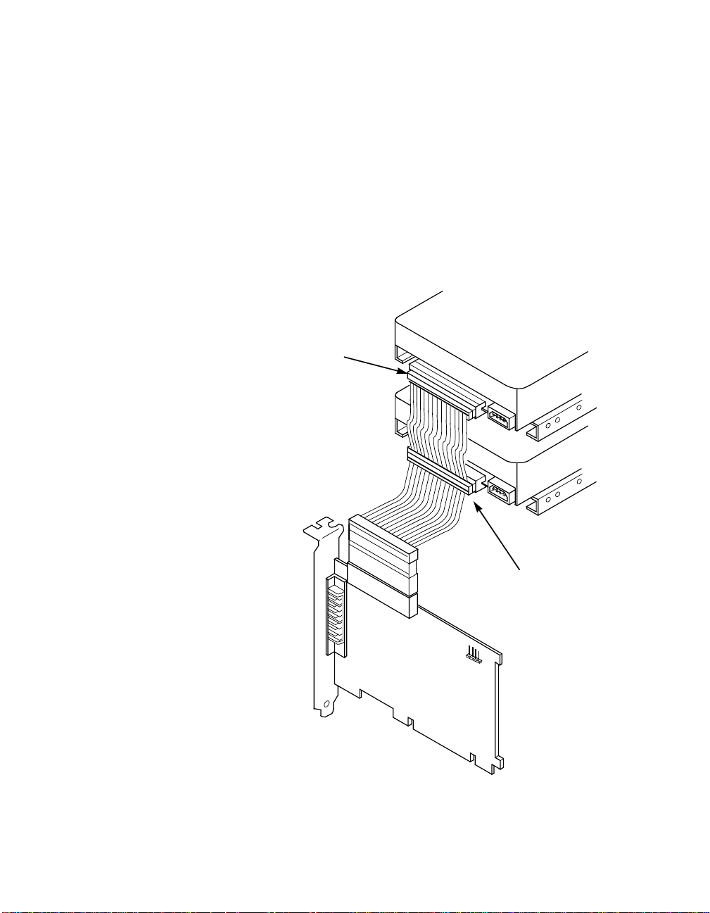
Step 1. To connect an internal SCSI device, plug the 68-pin connector
on one end of the internal SCSI ribbon cable into the connector
J2. Make certain to match pin 1 on both connectors. Figure 2.4
shows an example of this connection.
Figure 2.4 Internal SCSI Ribbon Cable to Host Adapter
Connection
Detailed Installation Procedure 2-7
Page 24
Step 2. Plug the 68-pin connector on the other end of the internal SCSI
ribbon cable into the SCSI connector on your internal SCSI
device. (See Figure 2.5.) Make sure to match pin 1 on all
connections.
Figure 2.5 Internal SCSI Ribbon Cable to Internal SCSI Device
Connection
Step 3. Connect additional internal SCSI devices by using an internal
SCSI ribbon cable with the required number of 68-pin
connectors attached along its length as shown in Figure 2.6.
Figure 2.6 Connecting Additional Internal SCSI Devices
2-8 Installing the LSI8751D
Page 25
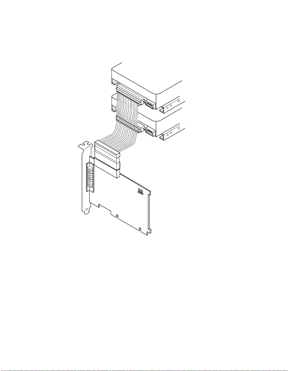
Figure 2.7 shows an example of this type of chained
connection. Make sure to match pin 1 on all connections.
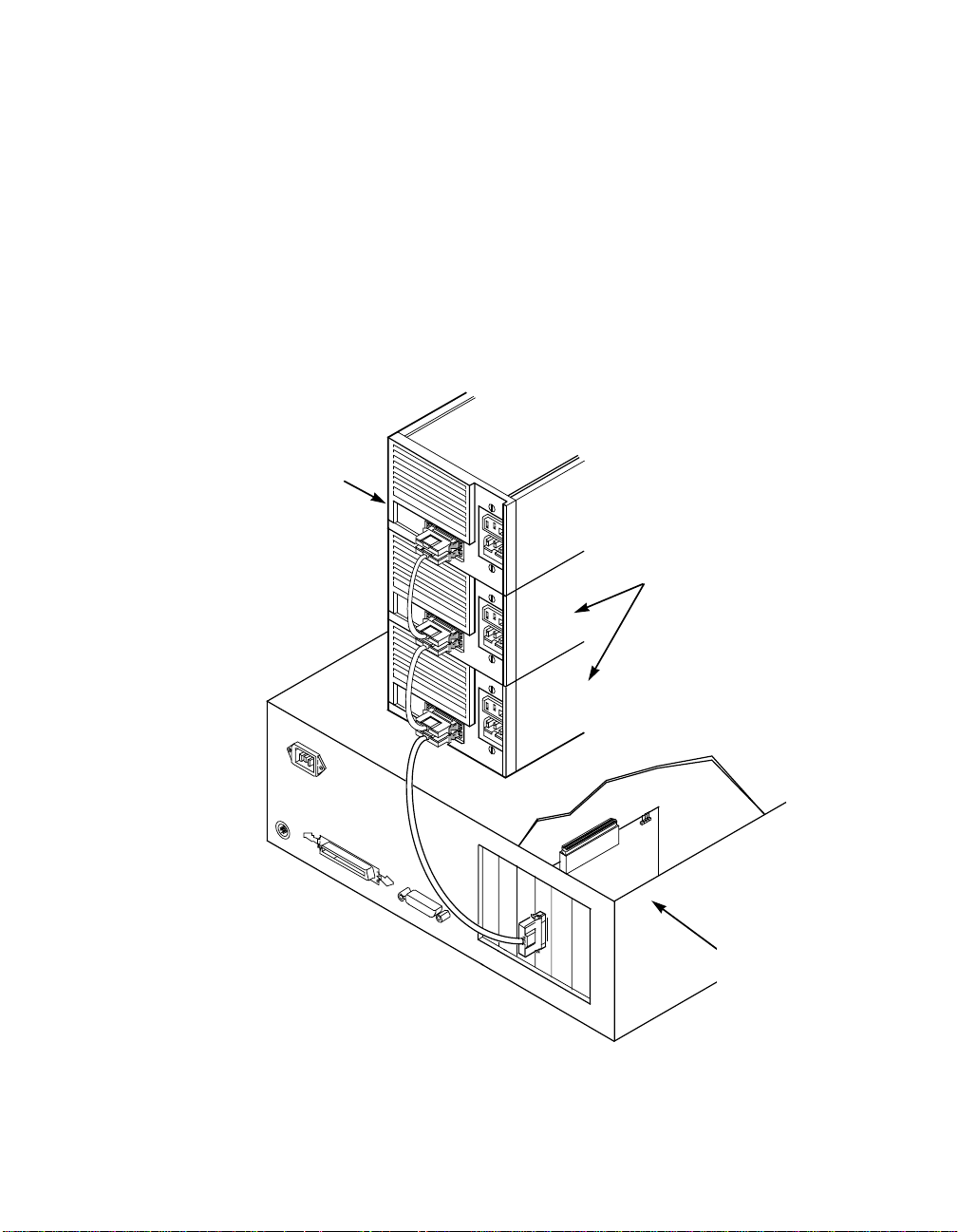
Figure 2.7 Multiple Internal SCSI Devices Chained Together
Detailed Installation Procedure 2-9
Page 26

Step 4. Most PC cabinets are designed with a front panel LED, which
may already be connected to an existing IDE drive. Connect
this LED cable to connector J4 on the host adapter, as shown
in Figure 2.8. This allows the front panel LED to indicate activity
on the SCSI bus. Connector J4 is not keyed. The orientation of
the LED cable does not matter as long as all four pins are
connected.
Figure 2.8 SCSI LED Connector
Connector J4
Some LED cables have only two wires. In this case, place the
connector on one end or the other of J4. If the LED does not light
during SCSI bus activity from this host adapter, you may have to
rotate the LED cable 180° on J4.
2-10 Installing the LSI8751D
Page 27
2.2.3.2 Making External SCSI Bus Connections
This section provides step-by-step instructions for making external SCSI
bus connections:
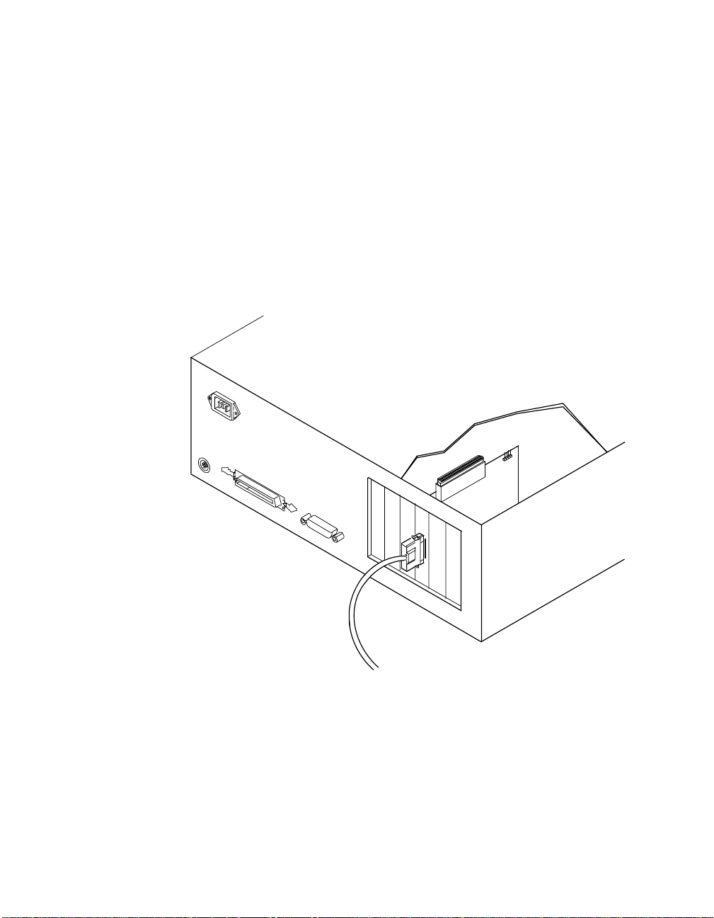
Step 1. To connect external SCSI devices to the LSI8751D, plug the 68-
pin connector on one end of a shielded external SCSI cable
(see Figure 2.3) into the host adapter connector J3 (see
Figure 2.1).
This connector is now bracketed to the back panel of your
computer. Figure 2.9 shows how this connection is made.
Figure 2.9 External Cable to Host Adapter
Detailed Installation Procedure 2-11
Page 28

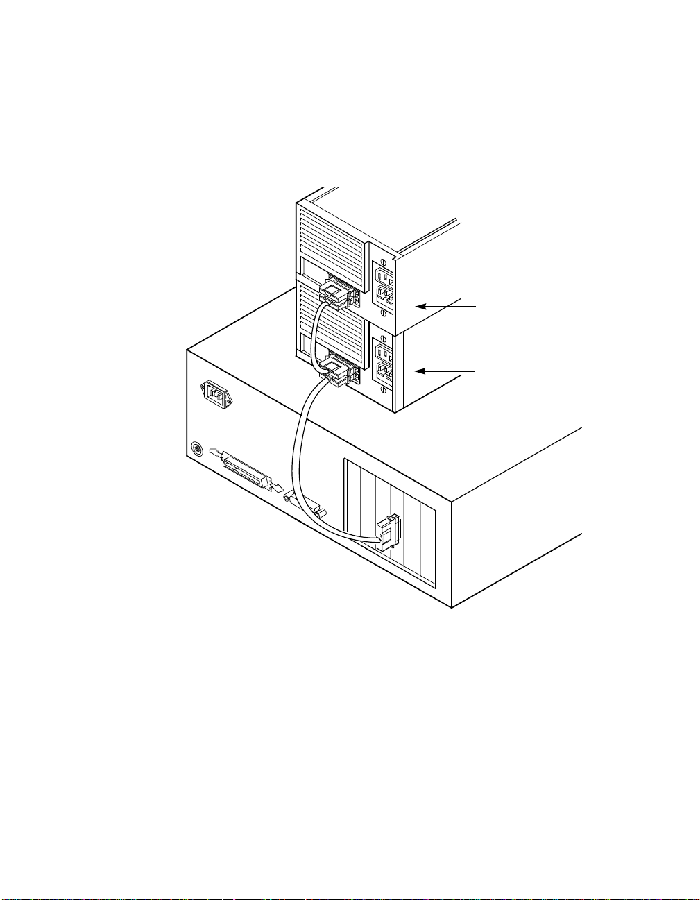
Step 2. Plug the 68-pin connector on the other end of the shielded
external SCSI cable into the SCSI connector on the external
SCSI device. Figure 2.10 shows an example of this connection.
Figure 2.10 External Cable to External SCSI Device
Terminator
External
Connector
2-12 Installing the LSI8751D
Page 29
Step 3. To connect more than one external SCSI device to the host
adapter, you must chain them together with shielded external
SCSI cables. Figure 2.11 shows an example of these chained
connections.
Figure 2.11 Multiple External SCSI Devices Chained Together
Termination Enabled
Termination Disabled
Detailed Installation Procedure 2-13
Page 30

2.2.4 SCSI Bus Termination
The devices making up the SCSI bus are connected serially (chained
together) with SCSI cables. The first and last physical SCSI devices
connected on the ends of the SCSI bus must have a set of resistors
called terminators. All other SCSI devices on the bus must have their
terminators removed or disabled. Remember that the LSI8751D is also
on the SCSI bus; if you position the host adapter at the end of the SCSI
bus, you must place the supplied HVD terminator on the unused
connector (J2 or J3).
The peripheral device terminators are usually set with jumpers, resistor
modules, or a switch on the peripheral. Refer to the peripheral
manufacturer’s instructions and to the user’s manual for your computer
for information on how to identify the terminator setting of each device
and how to change it.
The LSI8751D automatically covers SCSI bus termination for three
different bus configurations, depending on the use of the connectors J2
and J3 on the LSI8751D (see Figure 2.1). The three bus configurations
are
• only for internal SCSI connections to connector J2
• only for external SCSI connections to connector J3
• for SCSI connections to both J2 and J3 connectors
Termination on the LSI8751D for these three different bus configurations
is discussed in the following sections.
2-14 Installing the LSI8751D
Page 31
2.2.4.1 Internal SCSI Connections
If you make only internal SCSI device connections to the host adapter,
you must terminate the last internal device on the SCSI bus. You must
disable the termination on all other devices. Termination on the host
adapter is required in this case. Insert the plug-in HVD terminator into
the external connector J3 on the host adapter.
Figure 2.12 shows an example of how termination is determined for this
SCSI bus configuration.
Figure 2.12 Internal SCSI Device Termination
Last Device
Termination
on Chain –
Enabled
Does Not
End Chain –
Termination
Last Device on Chain –
Host Adapter Plug-in
HVD Terminator
Required on External
Connector J3
Disabled
Detailed Installation Procedure 2-15
Page 32
2.2.4.2 External SCSI Connections
If you make only external SCSI device connections to the host adapter,
you must terminate the last external device on the SCSI bus. You must
disable the termination on all other devices. Termination on the host
adapter is required in this case. Insert the plug-in HVD terminator into
the internal connector J2 on the host adapter.
Figure 2.13 shows you how to enable or disable termination for this SCSI
bus configuration.
Figure 2.13 External SCSI Device Termination
Last Device
on Chain –
Termination
Enabled
Does Not
End Chain –
Termination
Disabled
2-16 Installing the LSI8751D
Last Device
on Chain –
Host Adapter
Plug-in
HVD
Terminator
Required
on Internal
Connector J2
Page 33

2.2.4.3 Internal and External SCSI Connections
If you make internal and external SCSI device connections to the host
adapter, you must terminate the last internal device and external device
on the SCSI bus. You must disable the termination on all other devices.
Termination on the host adapter is not required in this case. Save the
plug-in HVD terminator so you can change the SCSI bus configuration in
the future.
Figure 2.14 shows you how to enable or disable termination for this SCSI
bus configuration.
Detailed Installation Procedure 2-17
Page 34
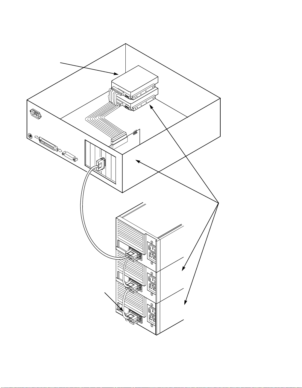
Figure 2.14 Internal and External SCSI Device Termination
Last Device
on Chain –
Termination
Enabled
Host Adapter
Termination
Not Required
Does Not
End Chain –
Termination
Disabled
Last Device
on Chain –
Termination
Enabled
2-18 Installing the LSI8751D
Page 35

2.2.5 Setting SCSI IDs
Each SCSI device and the host adapter must have a separate SCSI ID,
0 through 15. SCSI ID 7 is the preset host adapter setting, giving it the
highest priority on the SCSI bus. If you plan to boot your computer from
a SCSI hard disk drive on the SCSI bus, that drive should have SCSI ID
0, or the lowest SCSI ID on the bus. The PCI Storage Device
Management System SDMS 4.0 User’s Guide explains how to set your
host adapter ID using the SCSI BIOS Configuration Utility.
The peripheral device SCSI IDs are usually set with jumpers or with a
switch on the peripheral. Refer to the peripheral manufacturer’s
instructions and to the user’s manual for your computer to determine the
ID of each device and how to change it. No duplication of SCSI IDs is
allowed on a SCSI bus. Follow these steps for setting SCSI IDs:
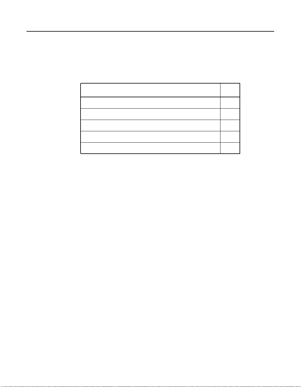
Step 1. Determine the SCSI ID of each device on the SCSI bus. Note
Step 2. Make any necessary changes to the SCSI IDs and record the
any duplications.
IDs for future reference. Correct any duplications at this time.
Table 2.2 is provided as a place to keep this record.
Detailed Installation Procedure 2-19
Page 36

Table 2.2 SCSI ID Record
SCSI ID SCSI Device
15
14
13
11
10
9
8
7
6
5
4
3
2
1
0
LSI8751D (default)
2-20 Installing the LSI8751D
Page 37
2.3 Completing the Installation
Before replacing the cover on your computer, review this installation
procedure check list. This can save you effort later.
Verify Installation Procedures Done
Host adapter connection in PCI bus slot secure
Internal SCSI bus connections secure (pin-1 continuity)
External SCSI bus connections secure
Proper SCSI bus termination established
Unique SCSI IDs set and recorded for each device
Step 1. Replace the cabinet cover on your computer.
Step 2. Plug in all power cords, and switch on power to all devices and
your computer.
Step 3. Wait for your computer to boot up.
Step 4. Refer to the PCI Storage Device Management System SDMS
4.0 User’s Guide (or the guide for the software you plan to use)
to load the driver software for your particular operating system.
To change the configuration of your host adapter, if needed,
refer to this same guide.
Completing the Installation 2-21
Page 38

2-22 Installing the LSI8751D
Page 39

Chapter 3
Technical
Specifications
This section discusses the physical environment associated with the
LSI8751D. The LSI8751D mechanical drawing is shown in Figure 1.1.
This section also includes these topics:
• Section 1.1, “Physical Environment,” page 1-1
• Section 1.2, “Operational Environment,” page 1-3
3.1 Physical Environment
This section discusses the physical, electrical, thermal, and safety
characteristics of the LSI8751D. This board complies with
electromagnetic standards set by the FCC.
3.1.1 Physical Characteristics
The dimensions of the LSI8751D are 5.00 x 3.25 inches (127 x 82.552
mm). PCI connection is made through the edge connector J1. Internal
SCSI connection is made through the 68-pin high density connector J2.
External SCSI connection is made through the 68-pin high density
connector J3. The J3 connector extends through the standard bracket,
which is attached to the face of the connector outside of the cabinet
where the LSI8751D is installed. The bracket is a standard type with a
cutout to accommodate connector J3. The J4 connector is for the Busy
LED connection using a 4-pin, one-row right-angle header. The
component height on the top and bottom of the board follows the PCI
specification.
LSI8751D PCI to SCSI Host Adapter 3-1
Page 40
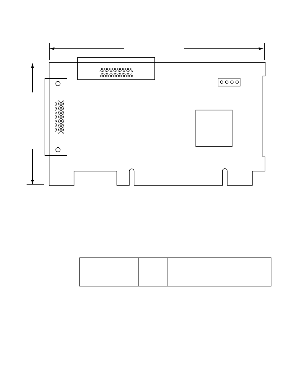
Figure 3.1 LSI8751D Mechanical Drawing
127.00 (REF) (5.00 (REF))
J2
J3
82.55 (REF) (3.25 (REF))
All dimensions are given in millimeters and (inches).
3.1.2 Electrical Characteristics
The LSI8751D maximum power requirements, including SCSI
TERMPWR, under normal operation, are shown in Table 1.1:
Table 3.1 Maximum Power Requirements
J4
LSI53C875J
J1
+5 V DC ±5% 1.5 A Over the operating range 5 °Cto55°C
+3.3 V DC ±0.3 V 130 mA Over the operating range 5 °Cto55°C
Under abnormal conditions, such as a short on SCSI TERMPWR, +5 V
current may be higher. At temperatures of at least 25 °C, a current of
4 A is sustained no longer than 30 seconds before the self-resetting
TERMPWR short circuit protection device opens.
3-2 Technical Specifications
when operating in a 3.3 V PCI slot
Page 41

The PCI PRSNT1/ and PRSNT2/ pins are set to indicate a 7.5 W
maximum configuration.
3.1.3 Thermal, Atmospheric Characteristics
The board operates in an environment defined by the following
parameters:
• Temperature range: 5 to 55 °C (dry bulb)
• Relative humidity range: 5 to 90% noncondensing
• Maximum dew point temperature: 32 °C
3.1.4 Electromagnetic Compliance
The board minimizes electromagnetic emissions, susceptibility to radio
frequency energy, and the effects of electromagnetic discharge. The
board meets the requirements of FCC and CISPR Class B limits and is
marked with the FCC Class B ID: B8J8251AD.
3.1.5 Safety Characteristics
The bare board meets or exceeds the requirements of UL flammability
rating 94 V0. The bare board is also marked with the supplier’s name or
trademark, type, and UL flammability rating. Because this board is
installed in a PCI bus slot, all voltages are below the SELV 42.4 V limit.
3.2 Operational Environment
The LSI8751D is designed for PCI computer systems with a standard
bracket. The SDMS software operates the board, but the design of the
board does not prevent the use of other software.
3.2.1 The PCI Interface
The PCI interface operates as a 32-bit DMA bus master. The connection
is made through the edge connector J1, which provides connections on
both the top and bottom of the board. The signal definitions and pin
numbers conform to the PCI Local Bus Specification Revision 2.1
standard. The signal assignments are shown in Table 1.2 and Table 1.3.
Operational Environment 3-3
Page 42

Note: The + 3.3 V pins are tied together and decoupled with high
frequency bypass capacitors to ground. No current from
these 3.3 V pins is used on the board. The PCI portion of
the LSI53C875J chip is powered from the 3 V/5 V pins.
Table 3.2 PCI Connector JI (Top)
Signal Name
-12 V 1 GND 17 C_BE2/ 33 GND 49
TCK 2 REQ/ 18 GND 34 KEYWAY 50
GND 3 3 V/5 V 19 IRDY/ 35 KEYWAY 51
TDO 4 AD31 20 +3.3 V 36 AD08 52
+5 V 5 AD29 21 DEVSEL/ 37 AD07 53
+5 V 6 GND 22 GND 38 +3.3 V 54
INTB/ 7 AD27 23 LOCK/ 39 AD05 55
INTD/ 8 AD25 24 PERR/ 40 AD03 56
GND (PRSNT1/) 9 +3.3 V 25 +3.3 V 41 GND 57
RESERVED 10 C_BE3/ 26 SERR/ 42 AD01 58
GND (PRSNT2/) 11 AD23 27 +3.3 V 43 3 V/5 V 59
KEYWAY 12 GND 28 C_BE1/ 44
KEYWAY 13 AD21 29 AD14 45 +5 V 61
RESERVED 14 AD19 30 GND 46 +5 V 62
1
Pin Signal Name1Pin Signal Name1Pin Signal Name1Pin
ACK64/ 60
GND 15 +3.3 V 31 AD12 47
CLK 16 AD17 32 AD10 48
1. Shaded signals are not connected.
3-4 Technical Specifications
Page 43
Table 3.3 PCI Connector JI (Bottom)
1
Signal Name
TRST/ 1 GNT/ 17 +3.3 V 33 AD09 49
+12V 2 GND 18 FRAME/ 34 KEYWAY 50
TMS 3 RESERVED 19 GND 35 KEYWAY 51
TDI 4 AD30 20 TRDY/ 36 C_BE0/ 52
+5 V 5 +3.3 V 21 GND 37 +3.3V 53
INTA/ 6 AD28 22 STOP/ 38 AD06 54
INTC/ 7 AD26 23 +3.3 V 39 AD04 55
+5 V 8 GND 24
RESERVED 9 AD24 25 SBO/ 41 AD02 57
3 V/5 V 10 IDSEL 26 GND 42 AD00 58
RESERVED 11 +3.3 V 27 PAR 43 3 V/5 V 59
KEYWAY 12 AD22 28 AD15 44
KEYWAY 13 AD20 29 +3.3 V 45 +5 V 61
RESERVED 14 GND 30 AD13 46 +5 V 62
Pin Signal Name
1
Pin Signal Name1Pin Signal Name1Pin
SDONE 40 GND 56
REQ64/ 60
RST/ 15 AD18 31 AD11 47
3 V/5 V 16 AD16 32 GND 48
1. Shaded signals are not connected.
3.2.2 The SCSI Interface
The SCSI interface operates as 16-bit, synchronous or asynchronous,
High Voltage Differential (HVD) bus, and supports SCSI-3 protocols and
16-bit arbitration. The signal definitions conform to the SCSI-2 differential
standard. The interface is made through connectors J2 and J3.
Connector J2 is a 68-pin, high density, right-angle receptacle used for
internal connections. Connector J3 is a 68-pin, high density, right-angle
receptacle that protrudes through the back panel bracket. SCSI
termination is provided through a HVD plug-in terminator. SCSI
termination power is also supplied by the board. Table Table 1.4 shows
the signal assignments for J2 and J3 SCSI HVD connectors.
Operational Environment 3-5
Page 44

Table 3.4 SCSI Connectors J2 and J3
Signal Name Pin Signal Name Pin Signal Name Pin Signal Name Pin
+DB(12) 1 TERMPWR 18 −DB(12) 35 TERMPWR 52
+DB(13) 2
+DB(14) 3 +ATN 20 −DB(14) 37 -ATN 54
+DB(15) 4 GND 21 −DB(15) 38 GND 55
+DB(P1) 5 +BSY 22 −DB(P1) 39 −BSY 56
GND 6 +ACK 23 GND 40 −ACK 57
+DB(0) 7 +RST 24 −DB(0) 41 −RST 58
+DB(1) 8 +MSG 25 −DB(1) 42 −MSG 59
+DB(2) 9 +SEL 26 −DB(2) 43 −SEL 60
+DB(3) 10 +C/D 27 −DB(3) 44 −C/D 61
+DB(4) 11 +REQ 28 −DB(4) 45 −REQ 62
+DB(5) 12 +I/O 29 −DB(5) 46 −I/O 63
+DB(6) 13 GND 30 −DB(6) 47 GND 64
+DB(7) 14 +DB(8) 31 −DB(7) 48 −DB(8) 65
+DB(P) 15 +DB(9) 32 −DB(P) 49 −DB(9) 66
DIFFSENS 16 +DB(10) 33 GND 50 −DB(10) 67
TERMPWR 17 +DB(11) 34 TERMPWR 51 −DB(11) 68
RESERVED 19 −DB(13) 36 RESERVED 53
3.2.3 The LED Interface
The LED interface on the LSI8751D is a four-wire arrangement that
allows the user to connect an LED harness to the board. The
GPIO0_FETCH line (maximum output low voltage 0.4 V and minimum
output low current 16 mA) is pulled low to complete the circuit when a
harness with an LED is attached. The connector on the LSI8751D is J4.
Table 3.5 LED Connector J4
Signal Name Pin
LED+ 1
LED− 2
LED− 3
LED+ 4
3-6 Technical Specifications
Page 45

Appendix A
Glossary of Terms and
Abbreviations
Active
Termination
Address A specific location in memory, designated either numerically or by a
Asynchronous
Data Transfer
BIOS Basic Input/Output System. Software that provides basic read/write
Bit A binary digit. The smallest unit of information a computer uses. The
Bus A collection of unbroken signal lines across which information is
Bus Mastering A high-performance way to transfer data. The host adapter controls the
The electrical connection required at each end of the SCSI bus,
composed of active voltage regulation and a set of termination resistors.
Ultra and Ultra2 SCSI require active termination.
symbolic name.
One of the ways data is transferred over the SCSI bus. It is slower than
synchronous data transfer.
capability. Usually kept as firmware (ROM based). The system BIOS on
the mainboard of a computer is used to boot and control the system. The
SCSI BIOS on your host adapter acts as an extension of the system
BIOS.
value of a bit (0 or 1) represents a two-way choice, such as on or off,
true or false, and so on.
transmitted from one part of a computer system to another. Connections
to the bus are made by way of taps on the lines.
transfer of data directly to and from system memory without interrupting
the computer’s microprocessor. This is the fastest way for multitasking
operating systems to transfer data.
Byte A unit of information consisting of eight bits.
CISPR A special international committee on radio interference (Committee,
International and Special, for Protection in Radio).
LSI8751D PCI to SCSI Host Adapter A-1
Page 46

Configuration Refers to the way a computer is set up; the combined hardware
components (computer, monitor, keyboard, and peripheral devices) that
make up a computer system; or the software settings that allow the
hardware components to communicate with each other.
CPU Central Processing Unit. The “brain” of the computer that performs the
actual computations. The term Microprocessor Unit (MPU) is also used.
DMA Direct Memory Access.
DMA Bus
Master
A feature that allows a peripheral to control the flow of data to and from
system memory by blocks, as opposed to PIO (Programmed I/O) where
the processor is in control and the flow is by byte.
Device Driver A program that allows a microprocessor (through the operating system)
to direct the operation of a peripheral device.
Differential SCSI A hardware configuration for connecting SCSI devices. It uses a pair of
lines for each signal transfer (as opposed to single-ended SCSI which
references each SCSI signal to a common ground). Two types of
differential signals in the industry are High Voltage Differential (HVD) and
Low Voltage Differential (LVD).
Dword A double word is a group of four consecutive bytes or characters that are
stored, addressed, transmitted, and operated on as a unit. The lower two
address bits of the least significant byte must equal zero in order to be
Dword aligned.
EEPROM Electronically Erasable Programmable Read Only Memory. A memory
chip typically used to store configuration information. See NVRAM.
EISA Extended Industry Standard Architecture. An extension of the 16-bit ISA
bus standard. It allows devices to perform 32-bit data transfers.
External SCSI
Device
A SCSI device installed outside the computer cabinet. These devices are
connected in a continuous chain using specific types of shielded cables.
Fast-20 The SCSI Trade Association (STA) supports the use of “Ultra SCSI” over
the term “Fast-20”. Please see Ultra SCSI.
Fast-40 The SCSI trade association (STA) supports the use of “Ultra2 SCSI” over
the term “Fast-40”. Please see Ultra2 SCSI.
A-2 Glossary of Terms and Abbreviations
Page 47

Fast SCSI A standard for SCSI data transfers. It allows a transfer rate of up to
10 Mbytes/s over an 8-bit SCSI bus and up to 20 Mbytes/s over a 16-bit
SCSI bus.
FCC Federal Communications Commission.
File A named collection of information stored on a disk.
Firmware Software that is permanently stored in ROM. Therefore, it can be
accessed during boot time.
Hard Disk A disk made of metal and permanently sealed into a drive cartridge. A
hard disk can store very large amounts of information.
Host The computer system in which a SCSI host adapter is installed. It uses
the SCSI host adapter to transfer information to and from devices
attached to the SCSI bus.
Host Adapter A circuit board or integrated circuit that provides a SCSI bus connection
to the computer system.
Internal SCSI
Device
A SCSI device installed inside the computer cabinet. These devices are
connected in a continuous chain using an unshielded ribbon cable.
IRQ Interrupt Request Channel. A path through which a device can get the
immediate attention of the computer’sCPU. The PCI bus assigns an IRQ
path for each SCSI host adapter.
ISA Industry Standard Architecture. A type of computer bus used in most
PCs. It allows devices to send and receive data up to 16-bits at a time.
Kbyte Kilobyte. A measure of computer storage equal to 1024 bytes.
Local Bus A way to connect peripherals directly to computer memory. It bypasses
the slower ISA and EISA buses. PCI is a local bus standard.
Logical Unit A subdivision, either logical or physical, of a SCSI device (actually the
place for the device on the SCSI bus). Most devices have only one
logical unit, but up to eight are allowed for each of the eight possible
devices on a SCSI bus.
LUN Logical Unit Number. An identifier, zero to seven, for a logical unit.
Glossary of Terms and Abbreviations A-3
Page 48

LVD SCSI Low Voltage Differential. LVD is a robust design methodology that
improves power consumption, data integrity, cable lengths and support
for multiple devices, while providinga migration path for increased I/O
performance.
Mainboard A large circuit board that holds RAM, ROM, the microprocessor, custom
integrated circuits, and other components that make a computer work. It
also has expansion slots for host adapters and other expansion boards.
Main Memory Thepart of a computer’s memory which is directly accessible by the CPU
(usually synonymous with RAM).
Mbyte Megabyte. A measure of computer storage equal to 1024 kilobytes.
Motherboard See Mainboard. In some countries, the term Motherboard is not
appropriate.
Multitasking The executing of more than one command at the same time. This allows
programs to operate in parallel.
Multithreading The simultaneous accessing of data by more than one SCSI device. This
increases the data throughput.
NVRAM NonVolatile Random Access Memory. Actually an EEPROM
(Electronically Erasable Read Only Memory chip) used to store
configuration information. See EEPROM.
Operating
System
A program that organizes the internal activities of the computer and its
peripheral devices. An operating system performs basic tasks such as
moving data to and from devices, and managing information in memory.
It also provides the user interface.
Parity Checking A way to verify the accuracy of data transmitted over the SCSI bus. The
parity bit in the transfer is used to make the sum of all the 1 bits either
odd or even (for odd or even parity). If the sum is not correct, the
information may be retransmitted or an error message may appear.
Passive
Termination
The electrical connection required at each end of the SCSI bus,
composed of a set of resistors. It improves the integrity of bus signals.
PCI Peripheral Component Interconnect. A local bus specification that allows
connection of peripherals directly to computer memory. It bypasses the
slower ISA and EISA buses.
A-4 Glossary of Terms and Abbreviations
Page 49

Peripheral
Devices
A piece of hardware (such as a video monitor, disk drive, printer, or
CD-ROM) used with a computer and under the computer’s control. SCSI
peripherals are controlled through a SCSI host adapter.
Pin-1
Orientation
The alignment of pin 1 on a SCSI cable connector and the pin-1 position
on the SCSI connector into which it is inserted. External SCSI cables are
always keyed to insure proper alignment, but internal SCSI ribbon cables
sometimes are not keyed.
PIO Programmed Input/Output. A way the CPU can transfer data to and from
memory using the computer’s I/O ports. PIO is usually faster than DMA,
but requires CPU time.
Port Address Also Port Number. The address through which commands are sent to a
host adapter board. This address is assigned by the PCI bus.
Port Number See Port Address.
Queue Tags A way to keep track of multiple commands that allow for increased
throughput on the SCSI bus.
RAM Random Access Memory. The computer’s primary working memory in
which program instructions and data are stored and are accessible to the
CPU. Information can be written to and read from RAM. The contents of
RAM are lost when the computer is turned off.
RISC Core LSI Logic SCSI chips contain a RISC (Reduced Instruction Set
Computer) processor, programmed through microcode scripts.
ROM Read Only Memory. Memory from which information can be read but not
changed. The contents of ROM are not erased when the computer is
turned off.
SCAM SCSI Configured AutoMatically. A method to automatically allocate SCSI
IDs using software when SCAM compliant SCSI devices are attached.
SCSI Small Computer System Interface. A specification for a high performance
peripheral bus and command set. The original standard is referred to as
SCSI-1.
SCSI-2 The current SCSI specification which adds features to the original
SCSI-1 standard.
SCSI-3 The SCSI specification which adds features to the SCSI-2 standard.
Glossary of Terms and Abbreviations A-5
Page 50

SCSI Bus A host adapter and one or more SCSI peripherals connected by cables
in a linear chain configuration. The host adapter may exist anywhere on
the chain, allowing connection of both internal and external SCSI
devices. A system may have more than one SCSI bus by using multiple
host adapters.
SCSI Device Any device that conforms to the SCSI standard and is attached to the
SCSI bus by a SCSI cable. This includes SCSI host adapters and SCSI
peripherals.
SCSI ID A way to uniquely identify each SCSI device on the SCSI bus. Each
SCSI bus has eight available SCSI IDs numbered 0 through 7 (or 0
through 15 for Wide SCSI). The host adapter usually gets the highest ID,
(7 or 15) giving it priority to control the bus.
SDMS Storage Device Management System. An LSI Logic software product that
manages SCSI system I/O.
Single-Ended
SCSI
A hardware specification for connecting SCSI devices. It references each
SCSI signal to a common ground. This is the most common method (as
opposed to differential SCSI which uses a separate ground for each
signal).
STA SCSI Trade Association. A group of companies that cooperate to
promote SCSI parallel interface technology as a viable mainstream I/O
interconnect for commercial computing.
Synchronous
Data Transfer
One of the ways data is transferred over the SCSI bus. Transfers are
clocked with fixed-frequency pulses. This is faster than asynchronous
data transfer. Synchronous data transfers are negotiated between the
SCSI host adapter and each SCSI device.
System BIOS Controls the low level POST (Power-On Self-Test), and basic operation
of the CPU and computer system.
Ultra SCSI A standard for SCSI data transfers. It allows a transfer rate of up to
20 Mbytes/s over a 8-bit SCSI bus and up to 40 Mbytes/s over a 16-bit
SCSI bus. STA (SCSI Trade Association) supports using the term “Ultra
SCSI” over the older term “Fast-20”.
Ultra2 SCSI A standard for SCSI data transfers. It allows a transfer rate of up to
40 Mbytes/s over an 8-bit SCSI bus, and up to 80 Mbytes/s over a
A-6 Glossary of Terms and Abbreviations
Page 51

16-bit SCSI bus. STA (SCSI Trade Association) supports using the term
“Ultra2 SCSI” over the term “Fast-40”.
VCCI Voluntary Control Council for Interference.
VDE Verband Deucher Elektroniker (Association of German Electrical
Engineers).
Virtual Memory Space on a hard disk that can be used as if it were RAM.
Wide SCSI A SCSI-2 feature allowing 16-bit or 32-bit transfers on the SCSI bus. This
dramatically increases the transfer rate over the standard 8-bit SCSI bus.
Wide Ultra SCSI The STA term for a SCSI bus width of 16 bits, with the SCSI bus speed
maximum data rate of 40 Mbytes/s.
Wide Ultra2
SCSI
The STA term for a SCSI bus width of 16 bits, with the SCSI bus speed
maximum data rate of 80 Mbytes/s.
Word A 2-byte (or 16-bit) unit of information.
Glossary of Terms and Abbreviations A-7
Page 52

A-8 Glossary of Terms and Abbreviations
Page 53

Index
B
board characteristics 1-3
C
chained connection 2-9, 2-13
completing the LSI8751D installation 2-21
connecting the SCSI peripherals 2-5
D
detailed installation procedure 2-2 to 2-12
duplication of SCSI IDs 2-19
E
edge connector 2-4
electrical characteristics 3-2
electromagnetic compliance 3-3
external SCSI bus connections 2-11
F
features 1-2
front panel LED 2-10
I
inserting the host adapter 2-3
installation procedure 2-2
installation procedure check list 2-21
internal SCSI bus connections 2-7
L
LED connector J4 3-6
LED interface 3-6
LSI8751D host adapter
board characteristics 1-3
features 1-2
installing 2-2 to 2-21
termination 1-2
Ultra SCSI 1-3
P
PCI connector J1 (bottom) 3-5
PCI connector J1 (top) 3-4
PCI interface 1-2
peripheral device SCSI IDs 2-19
, 3-3
Q
quick installation procedure 2-1 to 2-2
R
ribbon cable 2-5
S
safety characteristics 3-3
SCSI bus connections 2-5
SCSI bus termination 2-14
SCSI connector J3 3-5
SCSI ID record table 2-20
SCSI IDs 2-19
SCSI interface 1-2
SCSI peripherals 2-5
setting SCSI IDs 2-19
storage device management system (SDMS) 1-1
, 3-5
T
termination
SCSI bus 2-14 to 2-18
thermal, atmospheric characteristics 3-3
U
Ultra SCSI 1-3
O
operational environment 3-3
LSI8751D PCI to SCSI Host Adapter IX-1
Page 54

IX-2
Page 55

Customer Feedback
We would appreciate your feedback on this document. Please copy the
following page, add your comments, and fax it to us at the number
shown.
If appropriate, please also fax copies of any marked-up pages from this
document.
Important: Please include your name, phone number, fax number, and
company address so that we may contact you directly for
clarification or additional information.
Thank you for your help in improving the quality of our documents.
LSI8751D PCI to SCSI Host Adapter
Page 56

Reader’s Comments
Fax your comments to: LSI Logic Corporation
Technical Publications
M/S E-198
Fax: 408.433.4333
Please tell us how you rate this document: LSI8751D PCI to SCSI Host
Adapter. Place a check mark in the appropriate blank for each category.
Excellent Good Average Fair Poor
Completeness of information ____ ____ ____ ____ ____
Clarity of information ____ ____ ____ ____ ____
Ease of finding information ____ ____ ____ ____ ____
Technical content ____ ____ ____ ____ ____
Usefulness of examples and
illustrations
Overall manual ____ ____ ____ ____ ____
____ ____ ____ ____ ____
What could we do to improve this document?
If you found errors in this document, please specify the error and page
number. If appropriate, please fax a marked-up copy of the page(s).
Please complete the information below so that we may contact you
directly for clarification or additional information.
Name Date
Telephone
Fax
Title
Department Mail Stop
Company Name
Street
City, State, Zip
Customer Feedback
Page 57

You can find a current list of our U.S. distributors, international distributors, and sales
offices and design resource centers on our web site at
http://www.lsilogic.com/contacts/na_salesoffices.html
Page 58

Headquarters
Sales Offices
LSI Logic Corporation
North American Headquarters
Milpitas CA
Tel: 408.433.8000
Fax: 408.433.8989
LSI Logic Europe Ltd
European Headquarters
Bracknell England
Tel: 44.1344.426544
Fax: 44.1344.481039
LSI Logic K.K.
Headquarters
Tokyo Japan
Tel: 81.3.5463.7821
Fax: 81.3.5463.7820
 Loading...