

Page 1

TECHNICAL
MANUAL
LSI53C810A
PCI to SCSI I/O
Processor
Version 2.1
March 2001
®
S14067
Page 2

This document contains proprietary information of LSI Logic Corporation. The
information contained herein is not to be used by or disclosed to third parties
without the express written permission of an officer of LSI Logic Corporation.
LSI Logic products are not intended for use in life-support appliances, devices,
or systems. Use of any LSI Logic product in such applications without written
consent of the appropriate LSI Logic officer is prohibited.
Document DB14-000168-00, First Edition (March 2001)
This document describes the LSI Logic LSI53C810A PCI to SCSI I/O Processor
and will remain the official reference source for all revisions/releases of this
product until rescinded by an update.
To receive product literature, visit us at http://www.lsilogic.com.
LSI Logic Corporation reserves the right to make changes to any products herein
at any time without notice. LSI Logic does not assume any responsibility or
liability arising out of the application or use of any product described herein,
except as expressly agreed to in writing by LSI Logic; nor does the purchase or
use of a product from LSI Logic convey a license under any patent rights,
copyrights, trademark rights, or any other of the intellectual property rights of
LSI Logic or third parties.
Copyright © 1995–2001 by LSI Logic Corporation. All rights reserved.
TRADEMARK ACKNOWLEDGMENT
The LSI Logic logo design, TolerANT, SDMS, and SCRIPTS are registered
trademarks or trademarks of LSI Logic Corporation. All other brand and product
names may be trademarks of their respective companies.
ii
Page 3

Audience
Organization
Preface
This book is the primary reference and technical manual for the LSI Logic
LSI53C810A PCI to SCSI I/O Processor. It contains a complete
functional description for the product and includes complete physical and
electrical specifications.
This manual provides reference information on the LSI53C810A PCI to
SCSI I/O processor.It is intended forsystemdesigners and programmers
who are using this device to design a SCSI port for PCI-based personal
computers, workstations, or embedded applications.
This document has the following chapters and appendix:
• Chapter 1, General Description, includes general information about
the LSI53C810A and other members of the LSI53C8XX family of PCI
to SCSI I/O processors.
• Chapter 2, Functional Description, describes the main functional
areas of the chip in more detail, including the interfaces to the SCSI
bus.
• Chapter 3, PCI Functional Description, describes the chip’s
connection to the PCI bus, including the PCI commands and
configuration registers supported.
• Chapter 4, Signal Descriptions, contains the pin diagrams and
definitions of each signal.
• Chapter 5, Operating Registers, describes each bit in the operating
registers, organized by address.
Preface iii
Page 4

• Chapter 6, Instruction Set of the I/O Processor, defines all of the
• Chapter 7, Electrical Characteristics, contains the electrical
• Appendix A, Register Summary, is a register summary.
Related Publications
For background please contact:
ANSI
11 West 42nd Street
New York, NY 10036
(212) 642-4900
Ask for document number X3.131-199X (SCSI-2)
Global Engineering Documents
15 Inverness Way East
Englewood, CO 80112
(800) 854-7179 or (303) 397-7956 (outside U.S.) FAX (303) 397-2740
Ask for document number X3.131-1994 (SCSI-2) or X3.253
(SCSI-3 Parallel Interface)
SCSI SCRIPTS instructions that are supported by the LSI53C810A.
characteristics and AC timings for the chip.
ENDL Publications
14426 Black Walnut Court
Saratoga, CA 95070
(408) 867-6642
Document names:
SCSI Tutor
Prentice Hall
113 Sylvan Avenue
Englewood Cliffs, NJ 07632
(800) 947-7700
Ask for document number ISBN 0-13-796855-8,
the Small Computer System Interface
LSI Logic World Wide Web Home Page
www.lsil.com
iv Preface
SCSI Bench Reference, SCSI Encyclopedia,
SCSI: Understanding
Page 5

PCI Special Interest Group
2575 N. E. Katherine
Hillsboro, OR 97214
(800) 433-5177; (503) 693-6232 (International); FAX (503) 693-8344
SCSI SCRIPTS™ Processors Programming Guide,
S14044.A
Conventions Used in This Manual
The word
deassert
assert
means to drive a signal true or active. The word
means to drive a signal false or inactive.
Hexadecimal numbers are indicated by the prefix “0x” —for example,
0x32CF. Binary numbers are indicated by the prefix “0b” —for example,
0b0011.0010.1100.1111.
Revision Record
Revision Date Remarks
1.0 6/95 First version.
2.0 7/96 Revised technical manual.
2.1 3/01 All product names changed from SYM to LSI.
Order Number
Preface v
Page 6

vi Preface
Page 7

Contents
Chapter 1 General Description
1.1 TolerANT®Technology 1-2
1.2 LSI53C810A Benefits Summary 1-3
1.2.1 SCSI Performance 1-3
1.2.2 PCI Performance 1-4
1.2.3 Integration 1-4
1.2.4 Ease of Use 1-4
1.2.5 Flexibility 1-5
1.2.6 Reliability 1-5
1.2.7 Testability 1-6
Chapter 2 Functional Description
2.1 SCSI Core 2-1
2.1.1 DMA Core 2-2
2.2 SCRIPTS Processor 2-2
2.2.1 SDMS Software: The Total SCSI Solution 2-3
2.3 Prefetching SCRIPTS Instructions 2-3
2.3.1 Opcode Fetch Burst Capability 2-4
2.4 PCI Cache Mode 2-4
2.4.1 Load and Store Instructions 2-5
2.4.2 3.3 V/5 V PCI Interface 2-5
2.4.3 Loopback Mode 2-5
2.5 Parity Options 2-5
2.5.1 DMA FIFO 2-8
2.6 SCSI Bus Interface 2-11
2.6.1 Terminator Networks 2-11
2.6.2 Select/Reselect During Selection/Reselection 2-11
2.6.3 Synchronous Operation 2-13
Contents vii
Page 8

2.7 Interrupt Handling 2-15
2.7.1 Polling and Hardware Interrupts 2-15
Chapter 3 PCI Functional Description
3.1 PCI Addressing 3-1
3.1.1 Configuration Space 3-1
3.1.2 PCI Bus Commands and Functions Supported 3-2
3.2 PCI Cache Mode 3-3
3.2.1 Support for PCI Cache Line Size Register 3-3
3.2.2 Selection of Cache Line Size 3-4
3.2.3 Alignment 3-4
3.2.4 Memory Read Multiple Command 3-7
3.2.5 Unsupported PCI Commands 3-8
3.3 Configuration Registers 3-9
Chapter 4 Signal Descriptions
4.1 PCI Bus Interface Signals 4-5
4.1.1 System Signals 4-5
4.1.2 Address and Data Signals 4-6
4.1.3 Interface Control Signals 4-7
4.1.4 Arbitration Signals 4-8
4.1.5 Error Reporting Signals 4-8
4.2 SCSI Bus Interface Signals 4-9
4.2.1 SCSI Bus Interface Signals 4-9
4.2.2 Additional Interface Signals 4-10
Chapter 5 Operating Registers
Chapter 6 Instruction Set of the I/O Processor
6.1 Low Level Register Interface Mode 6-1
6.2 SCSI SCRIPTS 6-2
6.2.1 Sample Operation 6-3
6.3 Block Move Instructions 6-5
6.3.1 First Dword 6-6
6.3.2 Second Dword 6-12
6.4 I/O Instruction 6-13
viii Contents
Page 9

6.4.1 First Dword 6-13
6.4.2 Second Dword 6-22
6.5 Read/Write Instructions 6-23
6.5.1 First Dword 6-23
6.5.2 Second Dword 6-23
6.5.3 Read-Modify-Write Cycles 6-23
6.5.4 Move To/From SFBR Cycles 6-24
6.6 Transfer Control Instructions 6-27
6.6.1 First Dword 6-27
6.6.2 Second Dword 6-35
6.7 Memory Move Instructions 6-36
6.7.1 First Dword 6-38
6.7.2 Second Dword 6-38
6.7.3 Third Dword 6-38
6.7.4 Read/Write System Memory from a SCRIPTS
Instruction 6-39
6.8 Load and Store Instructions 6-39
6.8.1 First Dword 6-40
6.8.2 Second Dword 6-41
Chapter 7 Electrical Characteristics
7.1 DC Characteristics 7-1
7.2 TolerANT Technology 7-6
7.3 AC Characteristics 7-10
7.4 PCI Interface Timing Diagrams 7-12
7.4.1 Target Timing 7-13
7.4.2 Initiator Timing 7-17
7.5 PCI Interface Timing 7-26
7.6 SCSI Timings 7-27
7.7 Package Drawings 7-33
Appendix A Register Summary
Index
Customer Feedback
Contents ix
Page 10

Figures
1.1 LSI53C810A System Diagram 1-7
1.2 LSI53C810A Chip Block Diagram 1-8
2.1 DMA FIFO Sections 2-8
2.2 LSI53C810A Host Interface Data Paths 2-10
2.3 Active or Regulated Termination 2-12
2.4 Determining the Synchronous Transfer Rate 2-15
4.1 LSI53C810A Pin Diagram 4-2
4.2 Functional Signal Grouping 4-4
5.1 Register Address Map 5-2
6.1 SCRIPTS Overview 6-5
6.2 Block Move Instruction Register 6-8
6.3 I/O Instruction Register 6-16
6.4 Read/Write Register Instruction 6-25
6.5 Transfer Control Instruction 6-30
6.6 Memory to Memory Move Instruction 6-37
6.7 Load and Store Instruction Format 6-42
7.1 Rise and Fall Time Test Conditions 7-8
7.2 SCSI Input Filtering 7-8
7.3 Hysteresis of SCSI Receiver 7-8
7.4 Input Current as a Function of Input Voltage 7-9
7.5 Output Current as a Function of Output Voltage 7-9
7.6 Clock Timing 7-10
7.7 Reset Input 7-11
7.8 Interrupt Output Waveforms 7-11
7.9 PCI Configuration Register Read 7-13
7.10 PCI Configuration Register Write 7-14
7.11 Target Read 7-15
7.12 Target Write 7-16
7.13 OpCode Fetch, Nonburst 7-17
7.14 Burst Opcode Fetch 7-18
7.15 Back-to-Back Read 7-19
7.16 Back-to-Back Write 7-20
7.17 Burst Read 7-22
7.18 Burst Write 7-24
7.19 Initiator Asynchronous Send 7-27
7.20 Initiator Asynchronous Receive 7-28
x Contents
Page 11

Tables
7.21 Target Asynchronous Send 7-29
7.22 Target Asynchronous Receive 7-30
7.23 Initiator and Target Synchronous Transfers 7-30
7.24 100 LD PQFP (UD) Mechanical Drawing (Sheet 1 of 2) 7-34
2.1 Bits Used for Parity Control and Observation 2-6
2.2 SCSI Parity Control 2-7
2.3 SCSI Parity Errors and Interrupts 2-7
3.1 PCI Bus Commands and Encoding Types 3-9
3.2 PCI Configuration Register Map 3-10
4.1 Power and Ground Signals 4-3
4.2 System Signals 4-5
4.3 Address and Data Signals 4-6
4.4 Interface Control Signals 4-7
4.5 Arbitration Signals 4-8
4.6 Error Reporting Signals 4-8
4.7 SCSI Bus Interface Signals 4-9
4.8 Additional Interface Signals 4-10
5.1 Synchronous Clock Conversion Factor 5-10
5.2 Asynchronous Clock Conversion Factor 5-11
5.3 Examples of Synchronous Transfer Periods and
Rates for SCSI-1 5-13
5.4 Examples of Synchronous Transfer Periods and
Rates for Fast SCSI 5-14
5.5 SCSI Synchronous Offset Values 5-15
6.1 SCRIPTS Instructions 6-3
6.2 Read/Write Instructions 6-26
7.1 Absolute Maximum Stress Ratings 7-2
7.2 Operating Conditions 7-2
7.3 SCSI Signals—SD[7:0]/, SDP/, SREQ/, SACK/ 7-3
7.4 SCSI Signals—SMSG, SI_O/, SC_D/, SATN/, SBSY/,
SSEL/, SRST/ 7-3
7.5 Input Signals—CLK, SCLK, GNT/, IDSEL, RST/, TESTIN 7-3
7.6 Capacitance 7-4
7.7 Output Signals—MAC/_TESTOUT, REQ/ 7-4
7.8 Output Signal—IRQ/ 7-4
7.9 Output Signal—SERR/ 7-5
Contents xi
Page 12

7.10 Bidirectional Signals—AD[31:0], C_BE/[3:0], FRAME/,
IRDY/, TRDY/, DEVSEL/, STOP/, PERR/, PAR/ 7-5
7.11 Bidirectional Signals—GPIO0_FETCH/,
GPIO1_MASTER/ 7-6
7.12 TolerANT Technology Electrical Characteristics 7-7
7.13 Clock Timing 7-10
7.14 Reset Input Timing 7-11
7.15 Interrupt Output 7-11
7.16 PCI Timing 7-26
7.17 Initiator Asynchronous Send (5 Mbytes/s) 7-27
7.18 Initiator Asynchronous Receive (5 Mbytes/s) 7-28
7.19 Target Asynchronous Send (5 Mbytes/s) 7-29
7.20 Target Asynchronous Receive (5 Mbytes/s) 7-30
7.21 SCSI-1 Transfers (SE, 5.0 Mbytes/s) 7-31
7.22 SCSI-2 Fast Transfers (10.0 Mbytes/s (8-Bit Transfers),
40 MHz Clock) 7-31
7.23 SCSI-2 Fast Transfers (10.0 Mbytes/s (8-Bit Transfers),
50 MHz Clock) 7-32
A.1 Configuration Registers A-1
A.2 SCSI Registers A-2
xii Contents
Page 13

Chapter 1
General Description
Chapter 1 is divided into the following sections:
• Section 1.1, “TolerANT
®
Technology”
• Section 1.2, “LSI53C810A Benefits Summary”
The LSI53C810A PCI to SCSI I/O processor brings high-performance I/O
solutions to host adapter, workstation, and general computer designs,
making it easy to add SCSI to any PCI system.
The LSI53C810A is a pin-for-pin replacement for the LSI53C810 PCI to
SCSI I/O processor. It performs fast SCSI transfers in Single-Ended (SE)
mode, and improves performance by optimizing PCI bus utilization.
The LSI53C810A integrates a high-performance SCSI core, a PCI bus
master DMA core, and the LSI Logic SCSI SCRIPTS™ processor to
meet the flexibility requirements of SCSI-1, SCSI-2, and future SCSI
standards. It is designed to implement multithreaded I/O algorithms with
a minimum of processor intervention, solving the protocol overhead
problems of previous intelligent and nonintelligent adapter designs.
The LSI53C810A is fully supported by the LSI Logic Storage Device
Management System (SDMS™), a software package that supports the
Advanced SCSI Protocol Interface (ASPI). SDMS software provides
BIOS and driver support for hard disk, tape, removable media products,
and CD-ROM under the major PC operating systems.
The LSI53C810A is packaged in a compact rectangular 100-pin Plastic
Quad Flat Pack (PQFP) package to minimize board space requirements.
It operates the SCSI bus at 5 Mbytes/s asynchronously or 10 Mbytes/s
synchronously, and bursts data to the host at full PCI speeds. The
LSI53C810A increases SCRIPTS performance and reduces PCI bus
overhead by allowing instruction prefetches of 4 or 8 Dwords.
LSI53C810A PCI to SCSI I/O Processor 1-1
Page 14

Software development tools are available to developers who use the
SCSI SCRIPTS language to create customized SCSI software
applications. The LSI53C810A allows easy firmware upgrades and is
supported by advanced SCRIPTS commands.
1.1 TolerANT®Technology
The LSI53C810A features TolerANT technology, which includes active
negation on the SCSI drivers and input signal filtering on the SCSI
receivers. Active negation actively drives the SCSI Request,
Acknowledge, Data, and Parity signals HIGH rather than allowing them
to be passively pulled up by terminators. Active negation is enabled by
setting bit 7 in the SCSI Test Three (STEST3) register.
TolerANT receiver technology improves data integrity in unreliable
cabling environments where other devices would be subject to data
corruption. TolerANT receivers filter the SCSI bus signals to eliminate
unwanted transitions, without the long signal delay associated with
RC-type input filters. This improved driver and receiver technology helps
eliminate double clocking of data, the single biggest reliability issue with
SCSI operations. The TolerANT input signal filtering is a built in feature
of all LSI Logic fast SCSI devices. On the LSI53C8XX family products,
the user may select a filtering period of 30 or 60 ns, with bit 1 in the SCSI
Test Two (STEST2) register.
The benefits of TolerANT technology include increased immunity to noise
when the signal is going HIGH, better performance due to balanced duty
cycles, and improvedfast SCSI transfer rates. In addition, TolerANT SCSI
devices do not cause glitches on the SCSI bus at power-up or
power-down, so other devices on the bus are also protected from data
corruption. TolerANT technology is compatible with both the Alternative
One and Alternative Two termination schemes proposed by the American
National Standards Institute.
1-2 General Description
Page 15

1.2 LSI53C810A Benefits Summary
This section provides an overview of the LSI53C810A features and
benefits. It contains these topics:
• SCSI Performance
• PCI Performance
• Integration
• Ease of Use
• Flexibility
• Reliability
• Testability
1.2.1 SCSI Performance
To improve SCSI performance, the LSI53C810A:
• Complies with PCI 2.1 specification
• Supports variable block size and scatter/gather data transfers
• Minimizes SCSI I/O start latency
• Performs complex bus sequences without interrupts, including
restore data pointers
• Reduces Interrupt Service Routine (ISR) overhead through a unique
interrupt status reporting method
• Performs fast SCSI bus transfers in SE mode
– up to 7 Mbytes/s asynchronous
– 10 Mbytes/s synchronous
• Increases performance of data transfers to and from the chip
registers with new load and store SCRIPTS instruction
• Supports target disconnect and later reselect with no interrupt to the
system processor
• Supports execution of multithreaded I/O algorithms in SCSI
SCRIPTS with fast I/O context switching
LSI53C810A Benefits Summary 1-3
Page 16

1.2.2 PCI Performance
To improve PCI performance, the LSI53C810A:
• Bursts 2, 4, 8, or 16 Dwords across PCI bus with 80-byte DMA FIFO
• Prefetches up to 8 Dwords of SCRIPTS instructions
• Supports 32-bit word data bursts with variable burst lengths.
• Bursts SCRIPTS opcode fetches across the PCI bus
• Performs zero wait-state bus master data bursts faster than
110 Mbytes/s (@ 33 MHz)
• Supports PCI Cache Line Size register
1.2.3 Integration
Features of the LSI53C810A which ease integration include:
• 3.3 V/5 V PCI interface
• Full 32-bit PCI DMA bus master
• DMA controller using Memory-to-Memory Move instructions
• High-performance SCSI core
• Integrated SCRIPTS processor
• Compact 100-pin PQFP packaging
1.2.4 Ease of Use
The LSI53C810A provides:
• Direct PCI-to-SCSI connection
• Reduced SCSI development effort
• Support for the ASPI software standard using SDMS software
• Compatibility with existing LSI53C7XX and LSI53C8XX family
SCRIPTS
• Direct connection to PCI and SCSI SE bus
• Development tools and sample SCSI SCRIPTS
• Maskable and pollable interrupts
1-4 General Description
Page 17

1.2.5 Flexibility
• Three programmable SCSI timers: Select/Reselect, Handshake-to-
Handshake, and General Purpose. The time-out period is
programmable from 100 µs to greater than 1.6 seconds
• SDMS software for complete PC-based operating system support
• Support for relative jump
• New SCSI Selected As ID (SSAID) bits for use when responding with
multiple IDs
The LSI53C810A provides:
• High level programming interface (SCSI SCRIPTS)
• Support for execution of tailored SCSI sequences from main system
RAM
• Flexible programming interface to tune I/O performance or to adapt
to unique SCSI devices
• Flexibility to accommodate changes in the logical I/O interface
definition
• Low level access to all registers and all SCSI bus signals
1.2.6 Reliability
• Fetch, Master, and Memory Access control pins
• Support for indirect fetching of DMA address and byte counts so that
SCRIPTS can be placed in a PROM
• Separate SCSI and system clocks
• Selectable IRQ pin disable bit
• Ability to route system clock to SCSI clock
Enhanced reliability features of the LSI53C810A include:
• 2 kV ESD protection on SCSI signals
• Typical 300 mV SCSI bus hysteresis
• Average operating supply current of 50 mA
• Protection against bus reflections due to impedance mismatches
LSI53C810A Benefits Summary 1-5
Page 18

1.2.7 Testability
• Controlled bus assertion times (reduces RFI, improves reliability, and
eases FCC certification)
• Latch-up protection greater than 150 mA
• Voltage feed-through protection (minimum leakage current through
SCSI pads)
• High proportion (> 25%) of pins power and ground
• Power and ground isolation of I/O pads and internal chip logic
• TolerANT technology, which provides:
– Active negation of SCSI Data, Parity, Request, and Acknowledge
signals for improved fast SCSI transfer rates.
– Input signal filtering on SCSI receivers improves data integrity,
even in noisy cabling environments.
The LSI53C810A provides improved testability through:
• Access to all SCSI signals through programmed I/O
• SCSI loopback diagnostics
• SCSI bus signal continuity checking
• Support for single step mode operation
• Test mode (AND tree) to check pin continuity to the board
A system diagram showing the connections of the LSI53C810A in a PCI
system is pictured in Figure 1.1. A block diagram of the LSI53C810A is
pictured in Figure 1.2.
1-6 General Description
Page 19
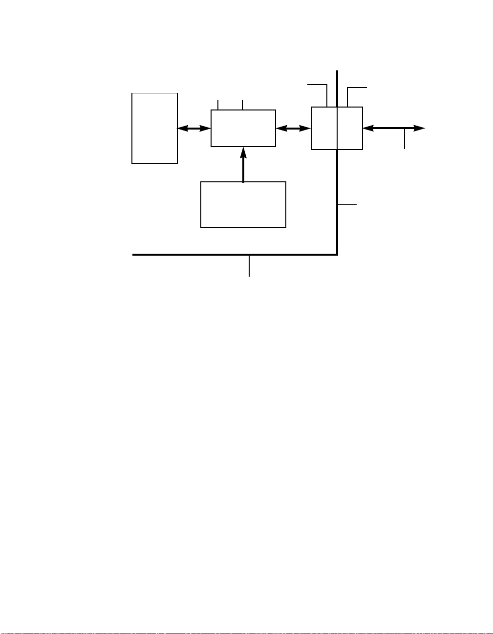
Figure 1.1 LSI53C810A System Diagram
SCSI Connection
V
V
DD
SS
PCI Bus LSI53C810A
40 MHz Oscillator or
Optional Internal
Connection to PCI
Bus Clock
CPU Baseboard
CPU Box
SCSI Term Connection
SCSI Bus
Peripheral
Bulkhead
LSI53C810A Benefits Summary 1-7
Page 20

Figure 1.2 LSI53C810A Chip Block Diagram
PCI
PCI Master and Slave Control Block
Data
FIFO
80 Bytes
SCSI
SCRIPTS
SCSI FIFO and SCSI Control Block
TolerANT Technology Drivers and Receivers
Operating
Registers
SE SCSI Bus
Configuration
Registers
1-8 General Description
Page 21

Chapter 2
Functional Description
Chapter 2 is divided into the following sections:
• Section 2.1, “SCSI Core”
• Section 2.2, “SCRIPTS Processor”
• Section 2.3, “Prefetching SCRIPTS Instructions”
• Section 2.4, “PCI Cache Mode”
• Section 2.5, “Parity Options”
• Section 2.6, “SCSI Bus Interface”
• Section 2.7, “Interrupt Handling”
The LSI53C810A contains three functional blocks: the SCSI Core, the
DMA Core, and the SCRIPTS Processor. The LSI53C810A is fully
supported by the SDMS, a complete software package that supports the
LSI Logic product line of SCSI processors and controllers.
2.1 SCSI Core
The SCSI core supports synchronous transfer rates up to 10 Mbytes/s
and asynchronous transfer rates up to 7 Mbytes/s on an 8-bit SCSI bus.
The SCSI core can be programmed with SCSI SCRIPTS, making it easy
to fine tune the system for specific mass storage devices or advanced
SCSI requirements.
The SCSI core offers low-level register access or a high-level control
interface. Like first generation SCSI devices, the LSI53C810A SCSI core
can be accessed as a register-oriented device. The ability to sample
and/or assert any signal on the SCSI bus can be used in error recovery
LSI53C810A PCI to SCSI I/O Processor 2-1
Page 22

2.1.1 DMA Core
and diagnostic procedures. In support of loopback diagnostics, the SCSI
core can perform a self-selection and operate as both an initiator and a
target.
The SCSI core is controlled by the integrated SCRIPTS processor
through a high-level logical interface. Commands controlling the SCSI
core are fetched out of the main host memory or local memory. These
commands instruct the SCSI core to Select, Reselect, Disconnect, Wait
for a Disconnect, Transfer Information, Change Bus Phases and, in
general, implement all aspects of the SCSI protocol. The SCRIPTS
processor is a special high-speed processor optimized for SCSI protocol.
The DMA core is a bus master DMA device that attaches directly to the
industry standard PCI bus. The DMA core is tightly coupled to the SCSI
core through the SCRIPTS processor, which supports uninterrupted
scatter/gather memory operations.
The LSI53C810A supports 32-bit memory and automatically supports
misaligned DMA transfers. An 80-byte FIFO allows 2, 4, 8, or 16 Dword
bursts across the PCI bus interface to run efficiently without throttling the
bus during PCI bus latency.
2.2 SCRIPTS Processor
The SCSI SCRIPTS processor allows both DMA and SCSI commands
to be fetched from host memory. Algorithms written in SCSI SCRIPTS
control the actions of the SCSI and DMA cores and are executed from
32-bit system RAM. The SCRIPTS processor executes complex SCSI
bus sequences independently of the host CPU.
The SCRIPTS processor can begin a SCSI I/O operation in
approximately 500 ns. This compares with 2–8 ms required for traditional
intelligent host adapters. Algorithms may be designed to tune SCSI bus
performance, to adjust to new bus device types (such as scanners,
communication gateways, etc.), or to incorporate changes in the SCSI-2
or SCSI-3 logical bus definitions without sacrificing I/O performance.
SCSI SCRIPTS are hardware independent, so they can be used
interchangeably on any host or CPU system bus.
2-2 Functional Description
Page 23

A complete set of development tools is available for writing custom
drivers with SCSI SCRIPTS. For more information on SCSI SCRIPTS
instructions supported by the LSI53C810A, see Chapter 6, “Instruction
Set of the I/O Processor.”
2.2.1 SDMS Software: The Total SCSI Solution
For users who do not need to develop custom drivers, LSI Logic provides
a total SCSI solution in PC environments with SDMS software. SDMS
software provides BIOS and driver support for hard disk, tape, and
removable media peripherals for the major PC-based operating systems.
SDMS software includes a SCSI BIOS to manage all SCSI functions
related to the device. It also provides a series of SCSI device drivers that
support most major operating systems. SDMS software supports a
multithreaded I/O application programming interface (API) for
user-developed SCSI applications. SDMS software supports both the
ASPI and CAM SCSI software specifications.
2.3 Prefetching SCRIPTS Instructions
When enabled by setting the Prefetch Enable bit (bit 5) in the DMA
Control (DCNTL) register, the prefetch logic in the LSI53C810A fetches
4 or 8 Dwords of instructions. The prefetch logic automatically
determines the maximum burst size that it can perform, based on the
burst length as determined by the values in the DMA Mode (DMODE)
register and the PCI Cache Line Size register (if cache mode is enabled).
If the unit cannot perform bursts of at least 4 Dwords, it disables itself.
The LSI53C810A may flush the contents of the prefetch unit under
certain conditions, listed below, to ensure that the chip always operates
from the most current version of the software. When one of these
conditions apply, the contents of the prefetch unit are automatically
flushed.
• On every Memory Move instruction. The Memory Move (MMOV)
instruction is often used to place modified code directly into memory.
To make sure that the chip executes all recent modifications, the
prefetch unit flushes its contents and loads the modified code every
time a MMOV instruction is issued. To avoid inadvertently flushing
Prefetching SCRIPTS Instructions 2-3
Page 24

the prefetch unit contents, use the No Flush Memory to Memory
Move (NFMMOV) instruction for all MMOV operations that do not
modify code within the next 4 to 8 Dwords. For more information on
this instruction, refer to Chapter 6, “Instruction Set of the I/O
Processor.”
• On every Store instruction. The Store instruction may also be used
to place modified code directly into memory. To avoid inadvertently
flushing the prefetch unit contents use the No Flush option for all
Store operations that do not modify code within the next 8 Dwords.
• On every write to the DMA SCRIPTS Pointer (DSP) register.
• On all Transfer Control instructions when the transfer conditions are
met. This is necessary because the next instruction to execute is not
the sequential next instruction in the prefetch unit.
• When the Prefetch Flush bit (DMA Control (DCNTL) bit 6) is set. The
unit flushes whenever this bit is set. The bit is self-clearing.
2.3.1 Opcode Fetch Burst Capability
Setting the Burst Opcode Fetch Enable bit (bit 1) in the DMA Mode
(DMODE) register (0x38) causes the LSI53C810A to burst in the first two
Dwords of all instruction fetches. If the instruction is a Memory-toMemory Move, the third Dword is accessed in a separate ownership. If
the instruction is an indirect type, the additional Dword is accessed in a
subsequent bus ownership. If the instruction is a Table Indirect Block
Move, the chip uses two accesses to obtain the four Dwords required, in
two bursts of two Dwords each.
Note: This feature can only be used if SCRIPTS prefetching is
disabled.
2.4 PCI Cache Mode
The LSI53C810A supports the PCI specification for an 8-bit Cache Line
Size register located in PCI configuration space. The Cache Line Size
register provides the ability to sense and react to nonaligned addresses
corresponding to cache line boundaries. In conjunction with the Cache
Line Size register, the PCI commands Read Line, Read Multiple, and
2-4 Functional Description
Page 25

Write and Invalidate are each software enabled or disabled to allow the
user full flexibility in using these commands. For more information on PCI
cache mode operations, refer to Chapter 3, “PCI Functional Description.”
2.4.1 Load and Store Instructions
The LSI53C810A supports the Load and Store instruction type, which
simplifies the movement of data between memory and the internal chip
registers. It also enables the LSI53C810A to transfer bytes to addresses
relative to the Data Structure Address (DSA) register. For more
information on the Load and Store instructions, refer to
Chapter 6, “Instruction Set of the I/O Processor.”
2.4.2 3.3 V/5 V PCI Interface
The LSI53C810A can attach directly to a 3.3 V or a 5 V PCI interface,
due to separate VDDpins for the PCI bus drivers. This allows the devices
to be used on the universal board recommended by the PCI Special
Interest Group.
2.4.3 Loopback Mode
The LSI53C810A loopback mode allows testing of both initiator and
target functions and, in effect, lets the chip communicate with itself.
When the Loopback Enable bit is set in the SCSI Test Two (STEST2)
register, bit 4, the LSI53C810A allows control of all SCSI signals whether
the chip is operating in the initiator or target mode. For more information
on this mode of operation refer to the
Programming Guide
.
SCSI SCRIPTS Processors
2.5 Parity Options
The LSI53C810A implements a flexible parity scheme that allows control
of the parity sense, allows parity checking to be turned on or off, and has
the ability to deliberately send a byte with bad parity over the SCSI bus
to test parity error recovery procedures. Table 2.1 defines the bits that
are involved in parity control and observation. Table 2.2 describes the
parity control function of the Enable Parity Checking and Assert SCSI
Even Parity bits in the SCSI Control Zero (SCNTL0) register. Table 2.3
describes the options available when a parity error occurs.
Parity Options 2-5
Page 26

Table 2.1 Bits Used for Parity Control and Observation
BIt Name Location Description
Assert SATN/ on Parity
Errors
Enable Parity Checking SCSI Control
Assert Even SCSI Parity SCSI Control
Disable Halt on SATN/or
a Parity Error (Target
Mode Only)
Enable Parity Error
Interrupt
Parity Error SCSI Interrupt
Status of SCSI Parity
Signal
Latched SCSI Parity SCSI Status One
SCSI Control
Zero (SCNTL0),
Bit 1
Zero (SCNTL0),
Bit 3
One (SCNTL1),
Bit 2
SCSI Control
One (SCNTL1),
Bit 5
SCSI Interrupt
Enable Zero
(SIEN0), Bit 0
Status Zero
(SIST0), Bit 0
SCSIStatusZero
(SSTAT0), Bit 0
(SSTAT1), Bit 3
Causes the LSI53C810Ato automatically assert SATN/
when it detects a parity error while operating as an
initiator.
Enables the LSI53C810A to check for parity errors.
The LSI53C810A checks for odd parity.
Determines the SCSI parity sense generated by the
LSI53C810A to the SCSI bus.
Causes the LSI53C810A not to halt operations when a
parity error is detected in target mode.
Determines whether the LSI53C810A generates an
interrupt when it detects a SCSI parity error.
This status bit is set whenever the LSI53C810A
detects a parity error on the SCSI bus.
This status bit represents the active HIGH current state
of the SCSI SDP0 parity signal.
This bit reflects the SCSI odd parity signal
corresponding to the data latched into the SCSI Input
Data Latch (SIDL) register.
Master Parity Error
Enable
Master Data Parity Error DMA Status
Master Data Parity Error
Interrupt Enable
Chip Test Four
(CTEST4), Bit 3
(DSTAT), Bit 6
DMA Interrupt
Enable (DIEN),
Bit 6
2-6 Functional Description
Enables parity checking during master data phases.
Set when the LSI53C810A, as a PCI master, detects a
target device signaling a parity error during a data
phase.
By clearing this bit, a Master Data Parity Error does not
cause assertion of IRQ/, but the status bit is set in the
DMA Status (DSTAT) register.
Page 27

Table 2.2 SCSI Parity Control
EPC AESP Description
0 0 Does not check for parity errors. Parity is generated when sending
0 1 Does not check for parity errors. Parity is generated when sending
1 0 Checks for odd parity on SCSI data received. Parity is generated
1 1 Checks for odd parity on SCSI data received. Parity is generated
1. Key:
EPC = Enable Parity Checking (bit 3, SCSI Control Zero (SCNTL0)).
ASEP = Assert SCSI Even Parity (bit 2, SCSI Control One (SCNTL1)).
SCSI data. Asserts odd parity when sending SCSI data.
SCSI data. Asserts even parity when sending SCSI data.
when sending SCSI data. Asserts odd parity when sending SCSI
data.
when sending SCSI data. Asserts even parity when sending SCSI
data.
Table 2.3 SCSI Parity Errors and Interrupts
DPH PAR Description
0 0 Halts when a parity error occurs in the target or initiator mode and
0 1 Halts when a parity error occurs in the target mode and generates
does not generate an interrupt.
an interrupt in target or initiator mode.
1 0 Does not halt in target mode when a parity error occurs until the
1 1 Does not halt in target mode when a parity error occurs until the
Key:
DHP = Disable Halt on SATN/ or Parity Error (bit 5, SCSI Control One (SCNTL1).
PAR = Parity Error (bit 0, SCSI Interrupt Enable Zero (SIEN0).
This table only applies when the Enable Parity Checking bit is set.
end of the transfer. An interrupt is not generated.
end of the transfer. An interrupt is generated.
Parity Options 2-7
Page 28
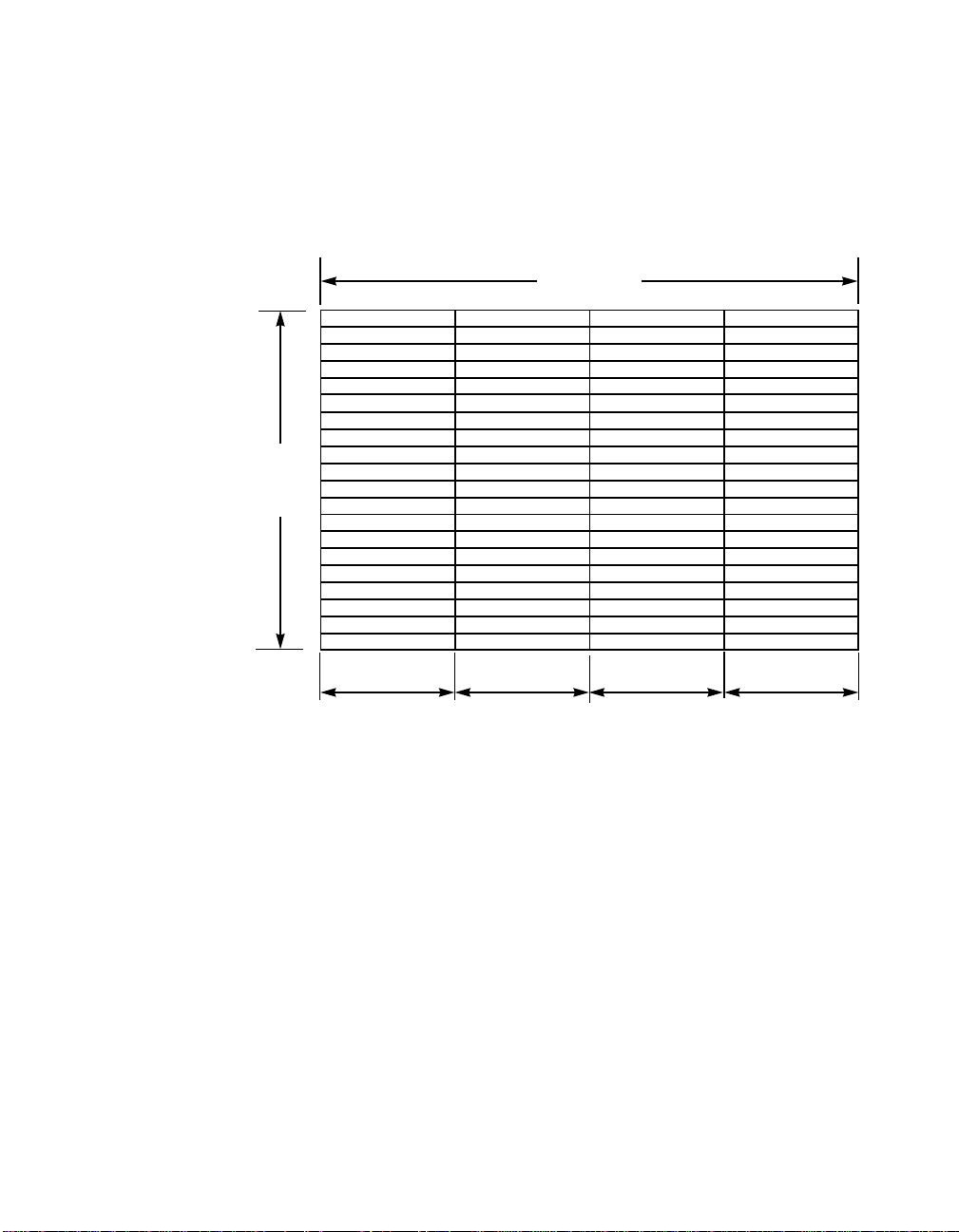
2.5.1 DMA FIFO
The DMA FIFO is divided into four sections, each one byte wide and
20 transfers deep. The DMA FIFO is illustrated in Figure 2.1.
Figure 2.1 DMA FIFO Sections
32-bits Wide
20
Bytes
Deep
8-bits
Byte Lane 3
2.5.1.1 Data Paths
The data path through the LSI53C810A is dependent on whether data is
being moved into or out of the chip, and whether SCSI data is being
transferred asynchronously or synchronously.
Figure 2.2 shows how data is moved to/from the SCSI bus in each of the
different modes.
The following steps determine if any bytes remain in the data path when
the chip halts an operation:
2-8 Functional Description
8-bits
Byte Lane 2
8-bits
Byte Lane 1
8-bits
Byte Lane 0
Page 29

Asynchronous SCSI Send –
Step 1. Look at the DMA FIFO (DFIFO) and DMA Byte Counter (DBC)
registers and calculate if there are bytes left in the DMA FIFO.
To make this calculation, subtract the seven least significant bits
of the DMA Byte Counter (DBC) register from the 7-bit value of
the DMA FIFO (DFIFO) register. AND the result with 0x7F for
a byte count between zero and 80.
Step 2. Read bit 5 in the SCSI Status Zero (SSTAT0) register to
determine if any bytes are left in the SCSI Output Data Latch
(SODL) register. If bit 5 is set in SSTAT0, then the SODL
register is full.
Synchronous SCSI Send –
Step 1. Look at the DMA FIFO (DFIFO) and DMA Byte Counter (DBC)
registers and calculate if there are bytes left in the DMA FIFO.
To make this calculation, subtract the seven least significant bits
of the DMA Byte Counter (DBC) register from the 7-bit value of
the DMA FIFO (DFIFO) register. AND the result with 0x7F for
a byte count between zero and 80.
Step 2. Read bit 5 in the SCSI Status Zero (SSTAT0) register to
determine if any bytes are left in the SCSI Output Data Latch
(SODL) register. If bit 5 is set in SSTAT0, then the SCSI Output
Data Latch (SODL) register is full.
Step 3. Read bit 6 in the SCSI Status Zero (SSTAT0) register to
determine if any bytes are left in the SODR register. If bit 6 is
set in SSTAT0, then the SODR register is full.
Asynchronous SCSI Receive –
Step 1. Look at the DMA FIFO (DFIFO) and DMA Byte Counter (DBC)
registers and calculate if there are bytes left in the DMA FIFO.
To make this calculation, subtract the seven least significant bits
of the DMA Byte Counter (DBC) register from the 7-bit value of
the DMA FIFO (DFIFO) register. AND the result with 0x7F for
a byte count between zero and 80.
Parity Options 2-9
Page 30
Step 2. Read bit 7 in the SCSI Status Zero (SSTAT0) register to
determine if any bytes are left in the SCSI Input Data Latch
(SIDL) register. If bit 7 is set in SSTAT0, then the SCSI Input
Data Latch (SIDL) register is full.
Synchronous SCSI Receive –
Step 1. Subtract the seven least significant bits of the DMA Byte
Counter (DBC) register from the 7-bit value of the DMA FIFO
(DFIFO) register. AND the result with 0x7F for a byte count
between zero and 80.
Step 2. Read the SCSI Status One (SSTAT1) register and examine bits
[7:4], the binary representation of the number of valid bytes in
the SCSI FIFO, to determine if any bytes are left in the SCSI
FIFO.
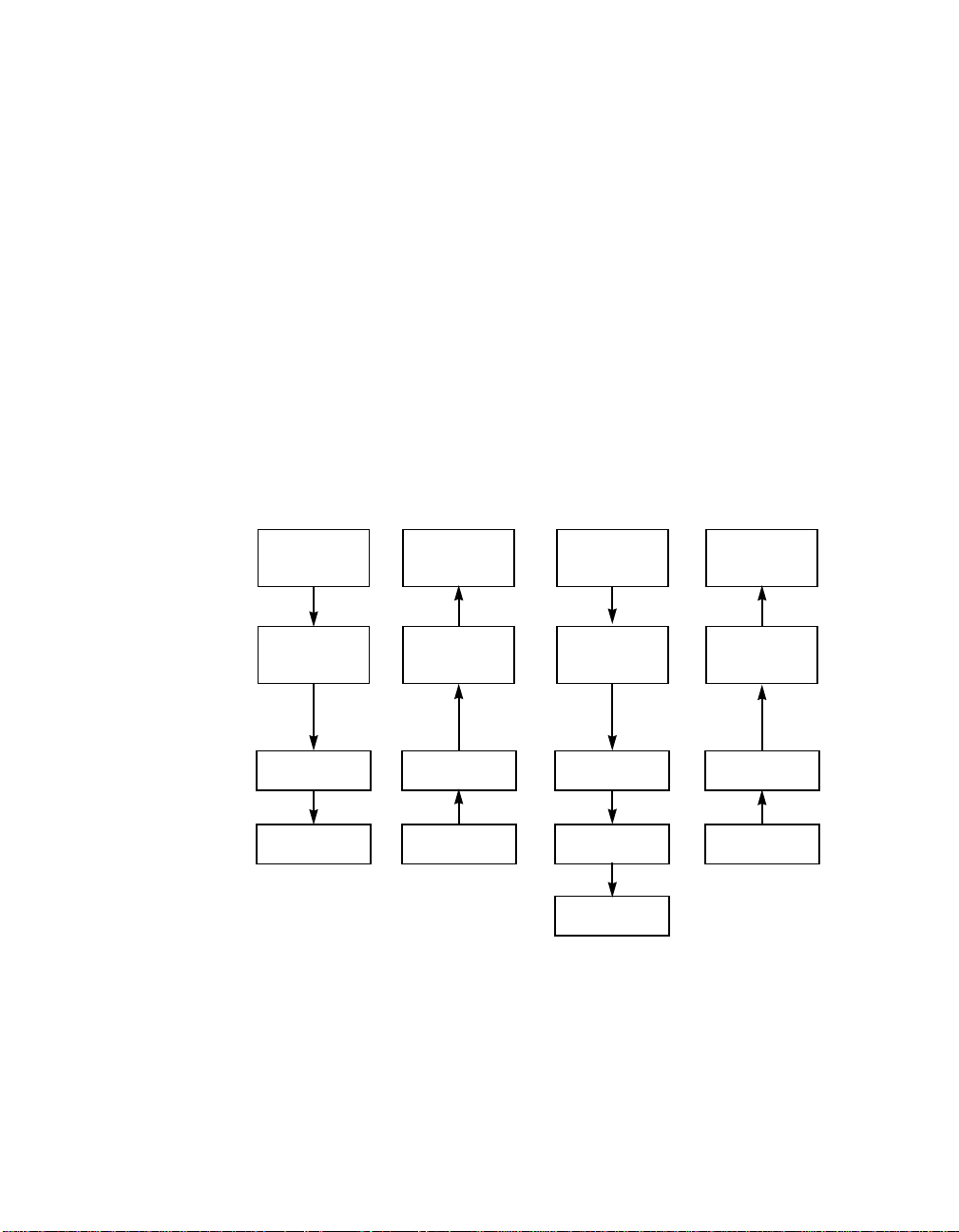
Figure 2.2 LSI53C810A Host Interface Data Paths
PCI
Interface
DMA FIFO
(4-bytes x 20)
SODL Register SIDL Register
Asynchronous
SCSI Send
PCI
Interface
DMA FIFO
(4-bytes x 20)
SCSI InterfaceSCSI Interface
Asynchronous
SCSI Receive
PCI
Interface
DMA FIFO
(4-bytes x 20)
SODL Register
SODR Register
SCSI Interface
Synchronous
SCSI Send
PCI
Interface
DMA FIFO
(4-bytes x 20)
SCSI FIFO
SCSI Interface
Synchronous
SCSI Receive
2-10 Functional Description
Page 31

2.6 SCSI Bus Interface
The LSI53C810A supports SE operation only. All SCSI signals are active
LOW. The LSI53C810A contains the SE output drivers and can be
connected directly to the SCSI bus. Each output is isolated from the
power supply to ensure that a powered-down LSI53C810A has no effect
on an active SCSI bus (CMOS “voltage feed-through” phenomena).
TolerANT technology provides signal filtering at the inputs of SREQ/ and
SACK/ to increase immunity to signal reflections.
2.6.1 Terminator Networks
The terminator networks provide the biasing needed to pull signals to an
inactive voltage level, and to match the impedance seen at the end of
the cable with the characteristic impedance of the cable. Terminators
must be installed at the extreme ends of the SCSI chain, and only at the
ends. No system should ever have more or less than two terminators
installed and active. SCSI host adapters should provide a means of
accommodating terminators. There should be a means of disabling the
termination.
SE cables can use a 220 Ω pull-up resistor to the terminator power
supply (Term-Power) line and a 330 Ω pull-down to ground. Because of
the high-performance nature of the LSI53C810A, regulated or active
termination is recommended. Figure 2.3 shows a Unitrode active
terminator. TolerANT active negation can be used with any ANSI
approved termination network. For additional information, refer to the
SCSI-2 specification.
2.6.2 Select/Reselect During Selection/Reselection
In multithreaded SCSI I/O environments, it is not uncommon to be
selected or reselected while trying to perform selection/reselection. This
situation may occur when a SCSI controller (operating in the initiator
mode) tries to select a target and is reselected by another. The Select
SCRIPTS instruction has an alternate address to which the SCRIPTS will
jump when this situation occurs. The analogous situation for target
devices is being selected while trying to perform a reselection.
SCSI Bus Interface 2-11
Page 32

Once a change in operating mode occurs, the initiator SCRIPTS should
start with a Set Initiator instruction or the target SCRIPTS should start
with a Set Target instruction. The Selection and Reselection Enable bits
(SCSI Chip ID (SCID) bits 5 and 6, respectively) should both be asserted
so that the LSI53C810A may respond as an initiator or as a target. If only
selection is enabled, the LSI53C810A cannot be reselected as an
initiator. There are also status and interrupt bits in the SCSI Interrupt
Status Zero (SIST0) and SCSI Interrupt Enable Zero (SIEN0) registers,
respectively, indicating that the LSI53C810A has been selected (bit 5) or
reselected (bit 4).
Figure 2.3 Active or Regulated Termination
UC5601QP
2.85V
C1
C2
Note:
1. C1 - 10 µF SMT
2. C2 - 0.1 µF SMT
3. J1 - 68-pin, high density “P” connector
2
REG_OUT
19
DISCONNECT
TERML1
TERML2
TERML3
TERML4
TERML5
TERML6
TERML7
TERML8
TERML9
TERML10
TERML11
TERML12
TERML13
TERML14
TERML15
TERML16
TERML17
TERML18
20
21
22
23
24
25
26
27
28
10
11
SD0 (J1.2)
SD1 (J1.4)
SD2 (J1.6)
SD3 (J1.8)
SD4 (J1.10)
SD5 (J1.12)
SD6 (J1.14)
SD7 (J1.16)
SD8 (J1.18)
3
4
5
6
7
8
9
ATN (J1.32)
BSY (J1.36)
ACK (J1.38)
RST (J1.40)
MSG (J1.42)
SEL (J1.44)
C/D (J1.46)
REQ (J1.48)
I/O (J1.50)
2-12 Functional Description
Page 33

2.6.3 Synchronous Operation
The LSI53C810A can transfer synchronous SCSI data in both the
initiator and target modes. The SCSI Transfer (SXFER) register controls
both the synchronous offset and the transfer period. It may be loaded by
the CPU before SCRIPTS execution begins, from within SCRIPTS using
a Table Indirect I/O instruction, or with a Read-Modify-Write instruction.
The LSI53C810A can receive data from the SCSI bus at a synchronous
transfer period as short as 80 ns or 160 ns (with a 50 MHz clock),
regardless of the transfer period used to send data. The LSI53C810A
can receive data at one-fourth of the divided SCLK frequency. Depending
on the SCLK frequency, the negotiated transfer period, and the
synchronous clock divider, the LSI53C810A can send synchronous data
at intervals as short as 100 ns for fast SCSI-2 and 200 ns for SCSI-1.
2.6.3.1 Determining the Data Transfer Rate
Synchronous data transfer rates are controlled by bits in two different
registers of the LSI53C810A. Following is a brief description of the bits.
Figure 2.4 illustrates the clock division factors used in each register, and
the role of the register bits in determining the transfer rate.
2.6.3.2 SCNTL3 Register, Bits [6:4] (SCF[2:0])
The SCF[2:0] bits select the factor by which the frequency of SCLK is
divided before being presented to the synchronous SCSI control logic.
The output from this divider controls the rate at which data can be
received; this rate must not exceed 50 MHz. The receive rate is
one-fourth of the divider output. For example, if SCLK is 40 MHz and the
SCF value is set to divide by one, then the maximum rate at which data
can be received is 10 Mbytes/s (40/(1*4) = 10).
For synchronous send, the output of the SCF divider is divided by the
transfer period (XFERP) bits in the SCSI Transfer (SXFER) register. For
valid combinations of the SCF and the XFERP, see Table 5.3 and
Table 5.4, under the description of the XFERP bits [7:5] in the SCSI
Transfer (SXFER) register.
SCSI Bus Interface 2-13
Page 34

2.6.3.3 SCNTL3 Register, Bits [2:0] (CCF[2:0])
The CCF[2:0] bits select the frequency of the SCLK for asynchronous
SCSI operations. To meet the SCSI timings as defined by the ANSI
specification, these bits need to be set properly.
2.6.3.4 SXFER Register, Bits [7:5] (TP[2:0])
The TP[2:0] divider (XFERP) bits determine the SCSI synchronous send
rate in either initiator or target mode. This value further divides the output
from the SCF divider.
2.6.3.5 Achieving Optimal SCSI Send Rates
To achieve optimal synchronous SCSI send timings, the SCF divisor
value should be set high, to divide the clock as much as possible before
presenting the clock to the TP divider bits in the SCSI Transfer (SXFER)
register. The TP[2:0] divider value should be as low as possible. For
example, with 40 MHz clock to achieve a Mbytes/s send rate, the SCF
bits can be set to divide by 1 and the TP bits to divide by 8; or the SCF
bits can be set to divide by 2 and the TP bits set to divide by 4. Use the
second option to achieve optimal SCSI timings.
2-14 Functional Description
Page 35

Figure 2.4 Determining the Synchronous Transfer Rate
SCF2 SCF1 SCF0 SCF
Divisor
0011
0 1 0 1.5
0112
1003
0003
SCLK
CCF2 CCF1 CCF0 SCSI Clock (MHz)
0 0 0 50.1-66.00
0 0 1 16.67-25.00
0 1 0 25.01-37.50
0 1 1 37.51-50.00
1 0 0 50.01-66.00
SCF
Divider
CCF
Divider
TP2 TP1 TP0 XFERP
Divisor
0004
0015
0106
0117
1008
1019
11010
11111
This point
must not
exceed
50 MHz
This point
must not
exceed
25 MHz
Example:
SCLK = 40 MHz, SCF = 1 (/1), XFERP = 0 (/4),
CCF = 3(37.51-50.00 MHz)
Synchronous send rate = (SCLK/SCF) /XFERP
= (40/1) /4 = 10 Mbytes/s
Synchronous receive rate = (SCLK/SCF) /4 =
(40/1) /4 = 10 Mbytes/s
Divide by 4
Synchronous
Divider
Asynchronous
SCSI Logic
Receive
Clock
Send Clock
(to SCSI Bus)
2.7 Interrupt Handling
The SCRIPTS processor in the LSI53C810A performs most functions
independently of the host microprocessor. However, certain interrupt
situations must be handled by the external microprocessor. This section
explains all aspects of interrupts as they apply to the LSI53C810A.
2.7.1 Polling and Hardware Interrupts
The external microprocessor is informed of an interrupt condition by
polling or hardware interrupts. Polling means that the microprocessor
must continually loop and read a register until it detects a bit set that
indicates an interrupt. This method is the fastest, but it wastes CPU time
Interrupt Handling 2-15
Page 36

2.7.1.1 Registers
that could be used for other system tasks. The preferred method of
detecting interrupts in most systems is hardware interrupts. In this case,
the LSI53C810A asserts the Interrupt Request (IRQ/) line that interrupts
the microprocessor, causing the microprocessor to execute an interrupt
service routine. A hybrid approach would use hardware interrupts for
long waits, and use polling for short waits.
The registers in the LSI53C810A that are used for detecting or defining
interrupts are the Interrupt Status (ISTAT), SCSI Interrupt Status Zero
(SIST0), SCSI Interrupt Status One (SIST1), DMA Status (DSTAT), SCSI
Interrupt Enable Zero (SIEN0), SCSI Interrupt Enable One (SIEN1), DMA
Control (DCNTL), and DMA Interrupt Enable (DIEN).
ISTAT – The ISTAT is the only register that can be accessed as a slave
during SCRIPTS operation. Therefore, it is the register that is polled
when polled interrupts are used. It is also the first register that should be
read after the IRQ/ pin is asserted in association with a hardware
interrupt. The INTF (Interrupt-on-the-Fly) bit should be the first interrupt
serviced. It must be written to one to be cleared. This interrupt must be
cleared before servicing any other interrupts.
If the SIP bit in the Interrupt Status (ISTAT) register is set, then a
SCSI-type interrupt has occurred and the SCSI Interrupt Status Zero
(SIST0) and SCSI Interrupt Status One (SIST1) registers should be read.
If the DIP bit in the Interrupt Status (ISTAT) register is set, then a
DMA-type interrupt has occurred and the DMA Status (DSTAT) register
should be read.
SCSI-type and DMA-type interrupts may occur simultaneously, so in
some cases both SIP and DIP may be set.
SIST0 and SIST1 – The SCSI Interrupt Status Zero (SIST0) and SCSI
Interrupt Status One (SIST1) registers contain the SCSI-type interrupt
bits. Reading these registers determines which condition or conditions
caused the SCSI-type interrupt, and clears that SCSI interrupt condition.
If the LSI53C810A is receiving data from the SCSI bus and a fatal
interrupt condition occurs, the LSI53C810A attempts to send the
contents of the DMA FIFO to memory before generating the interrupt.
2-16 Functional Description
Page 37

If the LSI53C810A is sending data to the SCSI bus and a fatal SCSI
interrupt condition occurs, data could be left in the DMA FIFO. Because
of this the DMA FIFO Empty (DFE) bit in DMA Status (DSTAT) should be
checked.
If this bit is cleared, set the CLF (Clear DMA FIFO) and CSF (Clear SCSI
FIFO) bits before continuing. The CLF bit is bit 2 in Chip Test Three
(CTEST3). The CSF bit is bit 1 in SCSI Test Three (STEST3).
DSTAT – The DMA Status (DSTAT) register contains the DMA-type
interrupt bits. Reading this register determines which condition or
conditions caused the DMA-type interrupt, and clears that DMA interrupt
condition. The DFE bit, bit 7 in DSTAT, is purely a status bit; it will not
generate an interrupt under any circumstances and will not be cleared
when read. DMA interrupts flush neither the DMA nor SCSI FIFOs before
generating the interrupt, so the DFE bit in the DMA Status (DSTAT)
register should be checked after any DMA interrupt.
If the DFE bit is cleared, then the FIFOs must be cleared by setting the
CLF (Clear DMA FIFO) and CSF (Clear SCSI FIFO) bits, or flushed by
setting the FLF (Flush DMA FIFO) bit.
SIEN0 and SIEN1 – The SCSI Interrupt Enable Zero (SIEN0) and SCSI
Interrupt Enable One (SIEN1) registers are the interrupt enable registers
for the SCSI interrupts in SCSI Interrupt Status Zero (SIST0) and SCSI
Interrupt Status One (SIST1).
DIEN – The DMA Interrupt Enable (DIEN) register is the interrupt enable
register for DMA interrupts in DMA Status (DSTAT).
DCNTL – When bit 1 in the DMA Control (DCNTL) register is set, the
IRQ/ pin is not asserted when an interrupt condition occurs. The interrupt
is not lost or ignored, but merely masked at the pin. Clearing this bit
when an interrupt is pending immediately causes the IRQ/ pin to assert.
As with any register other than ISTAT, this register cannot be accessed
except by a SCRIPTS instruction during SCRIPTS execution.
Interrupt Handling 2-17
Page 38

2.7.1.2 Fatal vs. Nonfatal Interrupts
A fatal interrupt, as the name implies, always causes SCRIPTS to stop
running. All nonfatal interrupts become fatal when they are enabled by
setting the appropriate interrupt enable bit. Interrupt masking is
discussed in Section 2.7.1.3, “Masking.” All DMA interrupts (indicated by
the DIP bit in ISTAT and one or more bits in DSTAT being set) are fatal.
Some SCSI interrupts (indicated by the SIP bit in the Interrupt Status
(ISTAT) and one or more bits in SCSI Interrupt Status Zero (SIST0) or
SCSI Interrupt Status One (SIST1) being set) are nonfatal.
When the LSI53C810A is operating in the Initiator mode, only the
Function Complete (CMP), Selected (SEL), Reselected (RSL), General
Purpose Timer Expired (GEN), and Handshake to Handshake Timer
Expired (HTH) interrupts are nonfatal.
When operating in the Target mode, CMP, SEL, RSL, Target mode:
SATN/ active (M/A), GEN, and HTH are nonfatal. Refer to the description
for the Disable Halt on a Parity Error or SATN/ active (Target Mode Only)
(DHP) bit in the SCSI Control One (SCNTL1) register to configure the
chip’s behavior when the SATN/ interrupt is enabled during Target mode
operation. The Interrupt-on-the-Fly interrupt is also nonfatal, since
SCRIPTS can continue when it occurs.
The reason for nonfatal interrupts is to prevent SCRIPTS from stopping
when an interrupt occurs that does not require service from the CPU.
This prevents an interrupt when arbitration is complete (CMP set), when
the LSI53C810A is selected or reselected (SEL or RSL set), when the
initiator asserts ATN (target mode: SATN/ active), or when the General
Purpose or Handshake-to-Handshake timers expire. These interrupts are
not needed for events that occur during high-level SCRIPTS operation.
2.7.1.3 Masking
Masking an interrupt means disabling or ignoring that interrupt. Interrupts
can be masked by clearing bits in the SCSI Interrupt Enable Zero
(SIEN0) and SCSI Interrupt Enable One (SIEN1) (for SCSI interrupts)
registers or the DMA Interrupt Enable (DIEN) (for DMA interrupts)
register. How the chip responds to masked interrupts depends on:
2-18 Functional Description
Page 39

whether polling or hardware interrupts are being used; whether the
interrupt is fatal or nonfatal; and whether the chip is operating in the
Initiator or Target mode.
If a nonfatal interrupt is masked and that condition occurs, the SCRIPTS
do not stop, the appropriate bit in the SCSI Interrupt Status Zero (SIST0)
or SCSI Interrupt Status One (SIST1) is still set, the SIP bit in the
Interrupt Status (ISTAT) is not set, and the IRQ/ pin is not asserted. See
Section 2.7.1.2, “Fatal vs. Nonfatal Interrupts,” for a list of the nonfatal
interrupts.
If a fatal interrupt is masked and that condition occurs, then the SCRIPTS
still stop, the appropriate bit in the DMA Status (DSTAT), SCSI Interrupt
Status Zero (SIST0),orSCSI Interrupt Status One (SIST1) register is
set, and the SIP or DIP bits in the Interrupt Status (ISTAT) is set, but the
IRQ/ pin is not asserted.
When the chip is initialized, enable all fatal interrupts if you are using
hardware interrupts. If a fatal interrupt is disabled and that interrupt
condition occurs, the SCRIPTS halt and the system never knows it
unless it times out and checks the ISTAT after a certain period of
inactivity.
If you are polling the ISTAT instead of using hardware interrupts, then
masking a fatal interrupt makes no difference since the SIP and DIP bits
in the Interrupt Status (ISTAT) inform the system of interrupts, not the
IRQ/ pin.
Masking an interrupt after IRQ/ is asserted does not cause deassertion
of IRQ/.
2.7.1.4 Stacked Interrupts
The LSI53C810A will stack interrupts if they occur one after the other. If
the SIP or DIP bits in the ISTAT register are set (first level), then there is
already at least one pending interrupt, and any future interrupts are
stacked in extra registers behind the SCSI Interrupt Status Zero (SIST0),
SCSI Interrupt Status One (SIST1), and DMA Status (DSTAT) registers
(second level). When two interrupts have occurred and the two levels of
the stack are full, any further interrupts set additional bits in the extra
registers behind SCSI Interrupt Status Zero (SIST0), SCSI Interrupt
Status One (SIST1), and DMA Status (DSTAT). When the first level of
Interrupt Handling 2-19
Page 40

interrupts are cleared, all the interrupts that came in afterward move into
SIST0, SIST1, and DSTAT. After the first interrupt is cleared by reading
the appropriate register, the IRQ/ pin is deasserted for a minimum of
three CLKs; the stacked interrupts move into SIST0, SIST1, or DSTAT;
and the IRQ/ pin is asserted once again.
Since a masked nonfatal interrupt does not set the SIP or DIP bits,
interrupt stacking does not occur. A masked, nonfatal interrupt still posts
the interrupt in SIST0, but does not assert the IRQ/ pin. Since no
interrupt is generated, future interrupts move into SCSI Interrupt Status
Zero (SIST0) or SCSI Interrupt Status One (SIST1) instead of being
stacked behind another interrupt. When another condition occurs that
generates an interrupt, the bit corresponding to the earlier masked
nonfatal interrupt is still set.
A related situation to interrupt stacking is when two interrupts occur
simultaneously. Since stacking does not occur until the SIP or DIP bits
are set, there is a small timing window in which multiple interrupts can
occur but are not stacked. These could be multiple SCSI interrupts (SIP
set), multiple DMA interrupts (DIP set), or multiple SCSI and multiple
DMA interrupts (both SIP and DIP set).
As previously mentioned, DMA interrupts do not attempt to flush the
FIFOs before generating the interrupt. It is important to set the Clear
DMA FIFO (CLF) and Clear SCSI FIFO (CSF) bits if a DMA interrupt
occurs and the DMA FIFO Empty (DFE) bit is not set. This is because
any future SCSI interrupts are not posted until the DMA FIFO is cleared
of data. These ‘locked out’ SCSI interrupts are posted as soon as the
DMA FIFO is empty.
2.7.1.5 Halting in an Orderly Fashion
When an interrupt occurs, the LSI53C810A attempts to halt in an orderly
fashion.
• If the interrupt occurs in the middle of an instruction fetch, the fetch
is completed, except in the case of a Bus Fault. Execution does not
begin, but the DMA SCRIPTS Pointer (DSP) points to the next
instruction since it is updated when the current instruction is fetched.
2-20 Functional Description
Page 41

• If the DMA direction is a write to memory and a SCSI interrupt
occurs, the LSI53C810A attempts to flush the DMA FIFO to memory
before halting. Under any other circumstances only the current cycle
is completed before halting, so the DFE bit in DMA Status (DSTAT)
should be checked to see if any data remains in the DMA FIFO.
• SCSI SREQ/SACK handshakes that have begun are completed
before halting.
• The LSI53C810A attempts to clean up any outstanding synchronous
offset before halting.
• In the case of Transfer Control Instructions, once instruction
execution begins it continues to completion before halting.
• If the instruction is a JUMP/CALL WHEN/IF <phase>, the DMA
SCRIPTS Pointer (DSP) is updated to the transfer address before
halting.
• All other instructions may halt before completion.
2.7.1.6 Sample Interrupt Service Routine
The following is a sample of an interrupt service routine for the
LSI53C810A. It can be repeated during polling or should be called when
the IRQ/ pin is asserted if hardware interrupts.
1. Read Interrupt Status (ISTAT).
2. If the INTF bit is set, it must be written to a one to clear this status.
3. If only the SIP bit is set, read SCSI Interrupt Status Zero (SIST0) and
SCSI Interrupt Status One (SIST1) to clear the SCSI interrupt
condition and get the SCSI interrupt status. The bits in the SIST0
and SIST1 tell which SCSI interrupt(s) occurred and determine what
action is required to service the interrupt(s).
4. If only the DIP bit is set, read the DMA Status (DSTAT) to clear the
interrupt condition and get the DMA interrupt status. The bits in
DSTATtell which DMA interrupts occurred and determine what action
is required to service the interrupts.
5. If both the SIP and DIP bits are set, read SCSI Interrupt Status Zero
(SIST0), SCSI Interrupt Status One (SIST1), and DMA Status
(DSTAT) to clear the SCSI and DMA interrupt condition and get the
interrupt status. If using 8-bit reads of the SIST0, SIST1, and DSTAT
registers to clear interrupts, insert a 12 CLK delay between the
Interrupt Handling 2-21
Page 42

consecutive reads to ensure that the interrupts clear properly. Both
the SCSI and DMA interrupt conditions should be handled before
leaving the ISR. It is recommended that the DMA interrupt is
serviced before the SCSI interrupt, because a serious DMA interrupt
condition could influence how the SCSI interrupt is acted upon.
6. When using polled interrupts, go back to Step 1 before leaving the
ISR, in case any stacked interrupts moved in when the first interrupt
was cleared. When using hardware interrupts, the IRQ/ pin will be
asserted again if there are any stacked interrupts. This should cause
the system to re-enter the ISR.
2-22 Functional Description
Page 43

Chapter 3
PCI Functional
Description
Chapter 3 is divided into the following sections:
• Section 3.1, “PCI Addressing”
• Section 3.2, “PCI Cache Mode”
• Section 3.3, “Configuration Registers”
3.1 PCI Addressing
There are three types of PCI-defined address space:
• Configuration space
• Memory space
• I/O space
3.1.1 Configuration Space
Configuration space is a contiguous 256-byte set of addresses dedicated
to each “slot” or “stub” on the bus. Decoding C_BE/[3:0] determines if a
PCI cycle is intended to access the configuration register space. The
IDSEL bus signal is a chip select that allows access to the configuration
register space only. Any attempt to access configuration space is ignored
unless IDSEL is asserted. The eight lower order address lines and byte
enables select a specific 8-bit register. The host processor uses this
configuration space to initialize the LSI53C810A.
The lower 128 bytes of the LSI53C810A configuration space hold system
parameters while the upper 128 bytes map into the LSI53C810A
operating registers. For all PCI cycles except configuration cycles, the
LSI53C810A registers are located on the 256-byte block boundary
defined by the base address assigned through the configured register.
LSI53C810A PCI to SCSI I/O Processor 3-1
Page 44

The LSI53C810A operating registers are available in both the upper and
lower 128-byte portions of the 256-byte space selected.
At initialization time, each PCI device is assigned a base address for
memory and I/O accesses. In the case of the LSI53C810A, the upper
24 bits of the address are selected. On every access, the LSI53C810A
compares its assigned base addresses with the value on the
Address/Data bus during the PCI address phase. If the upper 24 bits
match, the access is for the LSI53C810A and the low-order eight bits
define the register being accessed. A decode of C_BE/[3:0] determines
which registers and what type of access is to be performed.
I/O Space – The PCI specification defines I/O space as a contiguous
32-bit I/O address that is shared by all system resources, including the
LSI53C810A. Base Address Zero (I/O) determines which 256-byte I/O
area this device occupies.
Memory Space – The PCI specification defines memory space as a
contiguous 32-bit memory address that is shared by all system
resources, including the LSI53C810A. Base Address One (Memory)
determines which 256-byte memory area this device occupies.
3.1.2 PCI Bus Commands and Functions Supported
Bus commands indicate to the target the type of transaction the master
is requesting. Bus commands are encoded on the C_BE/[3:0] lines
during the address phase. PCI bus commands and encoding types
appear in Table 3.1.
3.1.2.1 I/O Read Command
The I/O Read command reads data from an agent mapped in I/O
address space. All 32 address bits are decoded.
3.1.2.2 I/O Write Command
The I/O Write command writes data to an agent when mapped in I/O
address space. All 32 address bits are decoded.
3-2 PCI Functional Description
Page 45

3.1.2.3 Memory Read Command
The Memory Read reads data from an agent mapped in memory
address space. All 32 address bits are decoded.
3.1.2.4 Memory Read Multiple Command
The Memory Read Multiple command reads data from an agent mapped
in memory address space. All 32 address bits are decoded.
3.1.2.5 Memory Read Line Command
The Memory Read Line command reads data from an agent mapped in
memory address space. All 32 address bits are decoded.
3.1.2.6 Memory Write Command
The Memory Write command writes data to an agent when mapped in
memory address space. All 32 address bits are decoded.
3.1.2.7 Memory Write and Invalidate Command
The Memory Write and Invalidate command writes data to an agent
when mapped in memory address space. All 32 address bits are
decoded.
3.2 PCI Cache Mode
The LSI53C810A supports the PCI specification for an 8-bit Cache Line
Size register located in PCI configuration space. The Cache Line Size
register provides the ability to sense and react to nonaligned addresses
corresponding to cache line boundaries. In conjunction with the Cache
Line Size register, the PCI commands Read Line, Read Multiple, and
Write and Invalidate are each software enabled or disabled to allow the
user full flexibility in using these commands.
3.2.1 Support for PCI Cache Line Size Register
The LSI3C810A supports the PCI specification for an 8-bit Cache Line
Size register in PCI configuration space. It can sense and react to
nonaligned addresses corresponding to cache line boundaries.
PCI Cache Mode 3-3
Page 46

3.2.2 Selection of Cache Line Size
The cache logic selects a cache line size based on the values for the
burst size in the DMA Mode (DMODE) register and the PCI Cache Line
Size register.
Note: The LSI53C810A does not automatically use the value in
the PCI Cache Line Size register as the cache line size
value. The chip scales the value of the Cache Line Size
register down to the nearest binary burst size allowed by
the chip (2, 4, 8 or 16), compares this value to the DMODE
burst size, then selects the smallest as the value for the
cache line size. The LSI53C810A uses this value for all
burst data transfers.
3.2.3 Alignment
The LSI53C810A uses the calculated burst size value to monitor the
current address for alignment to the cache line size. When it is not
aligned, the chip disables bursting allowing only single Dword transfers
until a cache line boundary is reached. When the chip is aligned, bursting
is re-enabled allowing bursts in increments specified by the Cache Line
Size register as explained above. If the Cache Line Size register is not
set (default = 0x00), the DMODE burst size is automatically used as the
cache line size.
3.2.3.1 MMOV Misalignment
The LSI53C810A does not operate in a cache alignment mode when a
MMOV instruction is issued and the read and write addresses are
different distances from the nearest cache line boundary. For example, if
the read address is 0x21F and the write address is 0x42F, and the cache
line size is eight (8), the addresses are byte aligned, but they are not the
same distance from the nearest cache boundary. The read address is 1
byte from the cache boundary 0x220 and the write address is 17 bytes
from the cache boundary 0x440. In this situation, the chip does not align
to cache boundaries and operates as an LSI53C810.
3-4 PCI Functional Description
Page 47

3.2.3.2 Memory Write and Invalidate Command
The Memory Write and Invalidate command is identical to the Memory
Write command, except that it additionally guarantees a minimum
transfer of one complete cache line; that is to say, the master intends to
write all bytes within the addressed cache line in a single PCI transaction
unless interrupted by the target. This command requires implementation
of the PCI Cache Line Size register at address 0x0C in PCI configuration
space. The LSI53C810A enables Memory Write and Invalidate cycles
when bit 0 (WRIE) in the Chip Test Three (CTEST3) register and bit 4
(WIE) in the PCI Command register are set. When the following
conditions are met, Memory Write and Invalidate commands are issued:
• The CLSE bit (Cache Line Size Enable, bit 7, DMA Control (DCNTL))
register), WRIE bit (Write and Invalidate Enable, bit 0, Chip Test
Three (CTEST3) register, and PCI configuration Command register,
bit 4 are set.
• The Cache Line Size register contains a legal burst size (2, 4, 8 or
16) value AND that value is less than or equal to the DMA Mode
(DMODE) burst size.
• The chip has enough bytes in the DMA FIFO to complete at least
one full cache line burst.
• The chip is aligned to a cache line boundary.
When these conditions are met, the LSI53C810A issues a Write and
Invalidate command instead of a Memory Write command during all PCI
write cycles.
Multiple Cache Line Transfers – When multiple cache lines of data
have been read in during a MMOV instruction (see the description for the
Read Multiple command), the LSI53C810A issues a Write and Invalidate
command using the burst size necessary to transfer all the data in one
transfer. For example, if the cache line size is 4, and the chip read in
16 Dwords of data using a Read Multiple command, the chip switches
the burst size to 16, and issues a Write and Invalidate to transfer all
16 Dwords in one bus ownership.
Latency – In accordance with the PCI specification, the latency timer is
ignored when issuing a Write and Invalidate command such that when a
latency time-out occurs, the LSI53C810A continues to transfer up until a
cache line boundary. At that point, the chip relinquishes the bus, and
PCI Cache Mode 3-5
Page 48

finish the transfer at a later time using another bus ownership. If the chip
is transferring multiple cache lines it continues to transfer until the next
cache boundary is reached.
PCI Target Retry – During a Write and Invalidate transfer, if the target
device issues a retry (STOP with no TRDY, indicating that no data was
transferred), the LSI53C810A relinquishes the bus and immediately tries
to finish the transfer on another bus ownership. The chip issues another
Write and Invalidate command on the next ownership, in accordance with
the PCI specification.
PCI Target Disconnect – During a Write and Invalidate transfer, if the
target device issues a disconnect the LSI53C810A relinquishes the bus
and immediately tries to finish the transfer on another bus ownership.
The chip does not issue another Write and Invalidate command on the
next ownership.
3.2.3.3 Memory Read Line Command
This command is identical to the Memory Read command, except that it
additionally indicates that the master intends to fetch a complete cache
line. This command is intended for use with bulk sequential data transfers
where the memory system and the requesting master might gain some
performance advantage by reading up to a cache line boundary rather
than a single memory cycle. The Read Line Mode function in the
LSI53C810A takes advantage of the PCI 2.1 specification regarding
issuing this command. The functionality of the Enable Read Line bit (bit 3
in DMA Mode (DMODE)) resembles the Write and Invalidate mode in
terms of conditions that must be met before a Read Line command is
issued. However, the Read Line option operates exactly like the previous
LSI53C8XX chips when cache mode has been disabled by a CLSE bit
reset or when certain conditions exist in the chip (explained below).
The Read Line mode is enabled by setting bit 3 in the DMA Mode
(DMODE) register. If cache mode is disabled, Read Line commands are
issued on every read data transfer, except opcode fetches.
3-6 PCI Functional Description
Page 49

If cache mode is enabled, a Read Line command is issued on all read
cycles, except opcode fetches, when the following conditions are met:
• The CLSE (Cache Line Size Enable, bit 7, DMA Control (DCNTL)
register) and ERL (Enable Read Line, bit 3, DMA Mode (DMODE)
register) bits are set.
• The Cache Line Size register must contain a legal burst size value
(2, 4, 8 or 16) and that value is less than or equal to the DMA Mode
(DMODE) burst size.
• The number of bytes to be transferred at the time a cache boundary
is reached must be equal to or greater than a full cache line size.
• The chip is aligned to a cache line boundary.
When these conditions are met, the chip issues a Read Line command
instead of a Memory Read during all PCI read cycles. Otherwise, it
issues a normal Memory Read command.
3.2.4 Memory Read Multiple Command
This command is identical to the Memory Read command except that it
additionally indicates that the master may intend to fetch more than one
cache line before disconnecting. The LSI53C810A supports PCI Read
Multiple functionality and issues Read Multiple commands on the PCI
bus when the Read Multiple Mode is enabled. This mode is enabled by
setting bit 2 (ERMP) of the DMA Mode (DMODE) register. The command
is issued when certain conditions are met.
If cache mode is enabled, a Read Multiple command is issued on all read
cycles, except opcode fetches, when the following conditions are met:
1. The CLSE bit (Cache Line Size Enable, bit 7, DMA Control (DCNTL)
register) and the ERMP bit (Enable Read Multiple, bit 2, DMA Mode
(DMODE) register) are set.
2. The Cache Line Size register contains a legal burst size value (2, 4,
8 or 16) and that value is less than or equal to the DMA Mode
(DMODE) burst size.
3. The number of bytes to be transferred at the time a cache boundary
is reached is equal to or greater than the DMA Mode (DMODE) burst
size.
4. The chip is aligned to a cache line boundary.
PCI Cache Mode 3-7
Page 50

When these conditions are met, the chip issues a Read Multiple
command instead of a Memory Read during all PCI read cycles.
Burst Size Selection – The Read Multiple command reads in multiple
cache lines of data in a single bus ownership. The number of cache lines
to read is determined by the DMA Mode (DMODE) burst size bits. In
other words, the chip switches its normal operating burst size to reflect
the DMA Mode (DMODE) burst size settings for the Read Multiple
command. For example, if the cache line size is 4, and the DMA Mode
(DMODE) burst size is 16, the chip switches the current burst size from
4 to 16, and issues a Read Multiple. After the transfer, the chip switches
the burst size back to the normal operating burst size of 4.
Read Multiple with Read Line Enabled – When both the Read
Multiple and Read Line modes are enabled, the Read Line command is
not issued if the above conditions are met. Instead, a Read Multiple
command is issued, even though the conditions for Read Line are met.
If the Read Multiple mode is enabled and the Read Line mode is
disabled, Read Multiple commands are issued if the Read Multiple
conditions are met.
3.2.5 Unsupported PCI Commands
The LSI53C810A does not respond to reserved commands, special
cycle, dual address cycle, or interrupt acknowledge commands as a
slave. It never generates these commands as a master.
PCI bus commands and encoding types appear in Table 3.1.
3-8 PCI Functional Description
Page 51

Table 3.1 PCI Bus Commands and Encoding Types
C_BE[3:0] Command Type Supported as Master Supported as Slave
0b0000 Interrupt Acknowledge No No
0b0001 Special Cycle No No
0b0010 I/O Read Yes Yes
0b0011 I/O Write Yes Yes
0b0100 Reserved N/A N/A
0b0101 Reserved N/A N/A
0b0110 Memory Read Yes Yes
0b0111 Memory Write Yes Yes
0b1000 Reserved N/A N/A
0b1001 Reserved N/A N/A
0b1010 Configuration Read No Yes
0b1011 Configuration Write No Yes
0b1100 Memory Read Multiple Yes No (defaults to 0110)
0b1101 Dual Address Cycle (DAC) No No
0b1110 Memory Read Line Yes No (defaults to 0110)
0b1111 Memory Write and Invalidate Yes No (defaults to 0111)
3.3 Configuration Registers
The Configuration registers are accessible only by system BIOS during
PCI configuration cycles, and are not available to the user at any time.
No other cycles, including SCRIPTS operations, can access these
registers.
The lower 128 bytes hold configuration data while the upper 128 bytes
hold the LSI53C810A operating registers, which are described in
Chapter 5, “Operating Registers.” The operating registers can be
accessed by SCRIPTS or the host processor.
Configuration Registers 3-9
Page 52

Note: The configuration register descriptions are provided for
general information only, to indicate which PCI
configuration addresses are supported in the LSI53C810A.
For detailed information, refer to the PCI Specification.
All PCI-compliant devices, such as the LSI53C810A, must support the
Vendor ID, Device ID, Command, and Status registers. Support of other
PCI-compliant registers is optional. In the LSI53C810A, registers that are
not supported are not writable and return all zeros when read. Only those
registers and bits that are currently supported by the LSI53C810A are
described in this chapter.
Table 3.2 contains a list of the PCI configuration registers supported in
the LSI53C810A. Addresses 0x40 through 0x7F are not defined.
Table 3.2 PCI Configuration Register Map
31 16 15 0
Device ID Vendor ID 0x00
Status Command 0x04
Class Code Revision ID 0x08
Not Supported Header Type Latency Timer Cache Line Size 0x0C
Base Address Zero (I/O)
Base Address One (Memory)
Not Supported 0x18
Not Supported 0x1C
Not Supported 0x20
Not Supported 0x24
Reserved 0x28
Reserved 0x2C
Reserved 0x30
Reserved 0x34
Reserved 0x38
Max_Lat Min_Gnt Interrupt Pin Interrupt Line 0x3C
1. I/O Base is supported.
2. Memory Base is supported.
Note: Addresses 0x40 to 0x7F are not defined. All unsupported registers are not writable and return all
zeros when read. Reserved registers also return zeros when read.
1
2
0x10
0x14
3-10 PCI Functional Description
Page 53

Register: 0x00
Vendor ID
Read Only
15 0
VID
1111000000000000
VID Vendor ID [15:0]
This field identifies the manufacturer of the device. The
Vendor ID is 0x1000.
Register: 0x02
Device ID
Read Only
15 0
DID
0000000000000000
DID Device ID [15:0]
This field identifies the particular device. The
LSI53C810A device ID is 0x0001.
Register: 0x04
Command
Read/Write
15 9 8 7 6 5 4 3 2 1 0
RSER EPER R WIE R EBM EMS EIS
0 0 0 0 0 0 00000000 00
The Command register provides coarse control over a device’s ability to
generate and respond to PCI cycles. When a zero is written to this
register, the LSI53C810A is logically disconnected from the PCI bus for
all accesses except configuration accesses.
In the LSI53C810A, bits 3, 5, 7, and 9 are not implemented. Bits 10
through 15 are reserved.
Configuration Registers 3-11
Page 54

R Reserved [15:9]
SE SERR/ Enable 8
This bit enables the SERR/ driver. SERR/ is disabled
when this bit is cleared. The default value of this bit is
zero. This bit and bit 6 must be set to report address
parity errors.
R Reserved 7
EPER Enable Parity Error Response 6
This bit allows the LSI53C810A to detect parity errors on
the PCI bus and report these errors to the system. Only
data parity checking is enabled. The LSI53C810A always
generates parity for the PCI bus.
R Reserved 5
WIE Write and Invalidate Mode 4
This bit, when set, will cause Memory Write and
Invalidate cycles to be issued on the PCI bus after certain
conditions have been met. For more information on these
conditions, refer to Section 3.2.3.2, “Memory Write and
Invalidate Command.” To enable Write and Invalidate
Mode, bit 0 in the Chip Test Three (CTEST3) register
(operating registers) must also be set.
R Reserved 3
EBM Enable Bus Mastering 2
This bit controls the ability of the LSI53C810y to act as a
master on the PCI bus. A value of zero disables the
device from generating PCI bus master accesses. A
value of one allows the LSI53C810A to behave as a bus
master. The LSI53C810A must be a bus master in order
to fetch SCRIPTS instructions and transfer data.
EMS Enable Memory Space 1
This bit controls the ability of the LSI53C810A to respond
to Memory Space accesses. A value of zero disables the
device response. A value of one allows the LSI53C810A
to respond to Memory Space accesses at the address
specified by Base Address One (Memory).
3-12 PCI Functional Description
Page 55

EIS Enable I/O Space 0
This bit controls the LSI53C810A’sresponse to I/O space
accesses. A value of zero disables the response. A value
of one allows the LSI53C810A to respond to I/O space
accesses at the address specified in Base Address Zero
(I/O).
Register: 0x06
Status
Read/Write
15 14 13 12 11 10 9 8 7 0
DPE SSE RMA RTA R DT[1:0] DPR R
000000000 0 0 0 0 0 0 0
The Status register is used to record status information for PCI
bus-related events.
In the LSI53C810A, bits 0 through 4 are reserved and bits 5, 6, 7, and
11 are not implemented.
Reads to this register behave normally. Writes are slightly different in that
bits can be cleared, but not set. A bit is cleared whenever the register is
written, and the data in the corresponding bit location is a one. For
instance, to clear bit 15 and not affect any other bits, write the value
0x8000 to the register.
DPE Detected Parity Error (from Slave) 15
This bit is set by the LSI53C810A whenever it detects a
data parity error, even if parity error handling is disabled.
SSE Signaled System Error 14
This bit is set whenever a device asserts the SERR/
signal.
RMA Master Abort (from Master) 13
A master device should set this bit whenever its
transaction (except for Special Cycle) is terminated with
master-abort. All master devices should implement this
bit.
Configuration Registers 3-13
Page 56

RTA Received Target Abort (from Master) 12
A master device should set this bit whenever its
transaction is terminated with a target abort. All master
devices should implement this bit.
R Reserved 11
DT[1:0] DEVSEL/ Timing [10:9]
These bits encode the timing of DEVSEL/.
0b00 Fast
0b01 Medium
0b10 Slow
0b11 Reserved
These bits are read only and should indicate the slowest
time that a device asserts DEVSEL/ for any bus
command except Configuration Read and Configuration
Write. The LSI53C810A supports 0b01.
DPR Data Parity Reported 8
This bit is set when the following three conditions are
met:
• The bus agent asserted PERR/ itself or observed
PERR/ asserted.
• The agent setting this bit acted as the bus master for
the operation in which the error occurred.
• The Parity Error Response bit in the Command
register is set.
R Reserved [7:0]
3-14 PCI Functional Description
Page 57

Register: 0x08
Revision ID
Read Only
7 0
RID
LSI53C810A
00100110
LSI53C810
00010100
RID Revision ID [7:0]
This register specifies device and revision identifiers. In
the LSI53C810A, the upper nibble is 0001b. The lower
nibble represents the current revision level of the device.
It should have the same value as the Chip Revision Level
bits in the Chip Test Three (CTEST3) register.
Register: 0x09
Class Code
Read Only
23 0
CC
000011110000000000000000
CC Class Code [23:0]
This register is used to identify the generic function of the
device. The upper byte of this register is a base class
code, the middle byte is a subclass code, and the lower
byte identifies a specific register level programming
interface. The value of this register is 0x010000, which
indicates a SCSI controller.
Configuration Registers 3-15
Page 58

Register: 0x0C
Cache Line Size
Read/Write
7 0
CLS
00000000
CLS Cache Line Size [7:0]
This register specifies the system cache line size in units
of 32-bit words. Cache mode is enabled and disabled by
the Cache Line Size Enable (CLSE) bit, bit 7 in the DMA
Control (DCNTL) register. Setting this bit causes the
LSI53C810A to align to cache line boundaries before
allowing any bursting, except during MMOVs in which the
read and write addresses are Burst Size boundary
misaligned. For more information see Section 3.2.1,
“Support for PCI Cache Line Size Register,” page 3-3.
Register: 0x0D
Latency Timer
Read/Write
7 0
00000000
LT Latency Timer [7:0]
The Latency Timer register specifies, in units of PCI bus
clocks, the value of the Latency Timer for this PCI bus
master. The LSI53C810A supports this timer. All eight
bits are writable, allowing latency values of 0–255 PCI
clocks. Use the following equation to calculate an
optimum latency value for the LSI53C810A:
Latency = 2 + (Burst Size * (typical wait states +1))
Values greater than optimum are also acceptable.
3-16 PCI Functional Description
LT
Page 59

Register: 0x0E
Header Type
Read Only
7 0
HT
00000000
HT Header Type [7:0]
This register identifies the layout of bytes 0x10 through
0x3F in configuration space and also whether or not the
device contains multiple functions. The value of this
register is 0x00.
Register: 0x10
Base Address Zero (I/O)
Read/Write
31 0
BARZ
xxxxxxxxxxxxxxxxxxxxxxxxxxxxxxx1
BARZ Base Address Register Zero (I/O) [31:0]
This 32-bit register has bit zero hardwired to one. Bit 1 is
reserved and must return a zero on all reads, and the
other bits are used to map the device into I/O space.
Register: 0x14
Base Address One (Memory)
Read/Write
31 0
BARO
xxxxxxxxxxxxxxxxxxxxxxxxxxxxxxx0
BARO Base Address Register One [31:0]
This register has bit 0 hardwired to zero. For detailed
information on the operation of this register, refer to the
PCI Specification.
Configuration Registers 3-17
Page 60

Register: 0x3C
Interrupt Line
Read/Write
7 0
IL
00000000
IL Interrupt Line [7:0]
This register is used to communicate interrupt line routing
information. POST software writes the routing information
into this register as it initiates and configures the system.
The value in this register tells which input of the system
interrupt controller(s) the device’s interrupt pin is
connected to. Values in this register are specified by
system architecture.
Register: 0x3D
Interrupt Pin
Read Only
7 0
IP
00000001
IP Interrupt Pin [7:0]
This register indicates which interrupt pin the device
uses. Its value is set to 0x01, for the INTA/ signal.
3-18 PCI Functional Description
Page 61

Register: 0x3E
Min_Gnt
Read Only
7 0
MG
00010001
MG Min_Gnt [7:0]
This register is used to specify the desired settings for
Latency Timer values. Min_Gnt is used to specify how
long a burst period the device needs. The value specified
in this register is in units of 0.25 microseconds. Values of
zero indicate that the device has no major requirements
for the settings of Latency Timers. The LSI53C810A sets
the Min_Gnt register to 0x11.
Register: 0x3F
Max_Lat
Read Only
7 0
ML
01000000
ML Max_Lat [7:0]
This register is used to specify the desired settings for
Latency Timer values. Max_Lat is used to specify how
often the device needs to gain access to the PCI bus.
The value specified in these registers is in units of
0.25 microseconds. Values of zero indicate that the
device has no major requirements for the settings of
Latency Timers. The LSI53C810A sets the Max_Lat
register to 0x40.
Configuration Registers 3-19
Page 62

3-20 PCI Functional Description
Page 63

Chapter 4
Signal Descriptions
This chapter presents the LSI53C810A pin configuration and signal
definitions using tables and illustrations. Figure 4.1 is the pin diagram
and Figure 4.2 is a functional signal grouping. The pin definitions are
presented in Table 4.1 through Table 4.8. The LSI53C810A is pin-for-pin
compatible with the LSI53C810. This chapter is divided into the following
sections:
• Section 4.1, “PCI Bus Interface Signals”
• Section 4.2, “SCSI Bus Interface Signals”
LSI53C810A PCI to SCSI I/O Processor 4-1
Page 64

Figure 4.1 LSI53C810A Pin Diagram
AD21
AD20
VDD-I
AD19
VSS-I
AD18
AD17
AD16
VSS-I
C_BE2/
FRAME/
IRDY/
VSS-I
TRDY/
DEVSEL/
VDD-I
STOP/
VSS-I
PERR/
PAR
C_BE1/
VSS-I
AD15
AD14
AD13
VSS-I
AD12
VDD-I
AD11
AD10
-I
SS
AD25
C_BE3/
IDSEL
AD22
V
AD24
AD23
95
97
99
100
1
2
3
4
5
6
7
8
9
10
11
12
13
14
15
16
17
18
19
20
21
22
23
24
25
26
27
28
29
30
323436384042444648
313335373941434547
-I
AD9
V
96
98
SS
AD8
AD7
C_BE0/
94
LSI53C810A
Quad Flat Pack
I
SS-
AD6
V
-I
-I
SS
V
V
AD27
AD26
91
93
90
92
100-pin
I
DD-
AD3
AD4
AD5
V
-C
AD30
86
AD0
AD31
85
-C
DD
V
DD
V
84
IRQ/
REQ/
83
-C
SS
V
81
82
80
CLK
79
RST/
SERR/
78
77
VDD-S
SD0/
76
75
SD1/
74
SD2/
VSS-S
73
72
SD3/
71
SD4/
70
SD5/
SD6/
69
68
VSS-S
SD7/
67
SDP/
66
65
SATN/
SBSY/
64
VSS-S
63
62
SACK/
61
SRST/
60
SMSG/
SSEL/
59
58
VSS-S
57
SCD/
56
SREQ/
55
SIO/
VDD-S
54
MAC/_TESTOUT
53
TESTIN
52
SCLK
51
50
49
-C
SS
V
DD
VSS-I
AD28
AD29
87
89
88
-I
SS
AD1
AD2
V
A slash (/) at the end of the signal name indicates that the active state
occurs when the signal is at a LOW voltage. When the slash is absent,
the signal is active at a HIGH voltage.
4-2 Signal Descriptions
GPIO0_FETCH/
GPIO1_MASTER/ GNT
Page 65

Signals are assigned a type. There are four signal types:
I Input, a standard input only signal.
O Output, a standard output driver (typically a Totem Pole Output).
T/S 3-state, a bidirectional, 3-state input/output signal.
S/T/S Sustained 3-state, an active LOW 3-state signal owned and driven by
one and only one agent at a time.
Table 4.1 describes the Power and Ground Signals group.
Table 4.1 Power and Ground Signals
Name Pin No. Description
V
SS-I
V
DD-I
V
SS-S
V
DD-S
V
SS-C
V
DD-C
1. These pins can accept a V
5, 9, 13, 18, 22, 26, 32, 37, 43,
Power supplies to the PCI I/O pins.
87, 93, 99
1
3, 16, 28, 40, 90 Power supplies to the PCI I/O pins.
58, 63, 68, 73 Power supplies to the SCSI bus I/O pins.
54, 77 Power supplies to the SCSI bus I/O pins.
50, 81 Power supplies to the internal logic core.
46, 84 Power supplies to the internal logic core.
source of 3.3 or 5 V. All other VDDpins must be supplied 5 V.
DD
4-3
Page 66

Figure 4.2 Functional Signal Grouping
System
Address
and
Data
Interface
Control
Arbitration
Error
Reporting
CLK
RST
AD[31:0]
C_BE/[3:0]
PAR
FRAME/
TRDY/
IRDY/
STOP/
DEVSEL/
IDSEL
REQ/
GNT/
PERR/
SERR/
SCLK
SD[7:0]
SDP
SCTRL/
TESTIN/
GPIO0_FETCH/
GPIO1_MASTER/
MAC/_TESTOUT
IRQ/
SCSI
Additional
Interface
4-4 Signal Descriptions
Page 67

4.1 PCI Bus Interface Signals
The PCI signal definitions are organized into the following functional
groups: Power and Ground Signals, System Signals, Address and Data
Signals, Interface Control Signals, Arbitration Signals, and Error
Reporting Signals.
4.1.1 System Signals
Table 4.2 describes the System Signals group.
Table 4.2 System Signals
Name Pin No. Type Description
CLK 80 I Clock provides timing for all transactions on the PCI bus and is an input to
RST/ 79 I Reset forces the PCI sequencer of each device to a known state. All T/S
every PCI device. All other PCI signals are sampled on the rising edge of
CLK, and other timing parameters are defined with respect to this edge.
Clock can optionally serve as the SCSI core clock, but this may effect fast
SCSI transfer rates.
and S/T/S signals are forced to a high impedance state, and all internal logic
is reset. The RST/ input is synchronized internally to the rising edge of CLK.
The CLK input must be active while RST/ is active to properly reset the
device.
PCI Bus Interface Signals 4-5
Page 68

4.1.2 Address and Data Signals
Table 4.3 describes the Address and Data Signals group.
Table 4.3 Address and Data Signals
Name Pin No. Type Description
AD[31:0] 85, 86, 88, 89,
91, 92, 94, 95,
98, 100, 1, 2, 4,
6, 7, 8, 23, 24,
25, 27, 29, 30,
31, 33, 35, 36,
38, 39, 41, 42,
44, 45
C_BE/[3:0] 96, 10, 21, 34 T/S Bus Command and Byte Enables are multiplexed on the
PAR 20 T/S Parity is the even parity bit that protects the AD[31:0] and
T/S Physical Dword Address and Data are multiplexed on the
same PCI pins. During the first clock of a transaction,
AD[31:0] contain a physical byte address. During subsequent
clocks, AD[31:0] contain data. A bus transaction consists of
an address phase followed by one or more data phases. PCI
supports both read and write bursts. AD[7:0] define the least
significant byte, and AD[31:24] define the most significant
byte.
same PCI pins. During the address phase of a transaction,
C_BE/[3:0] define the bus command. During the data phase,
C_BE/[3:0] are used as byte enables. The byte enables
determine which byte lanes carry meaningful data. C_BE/[0]
applies to byte 0, and C_BE/[3] to byte 3.
C_BE/[3:0] lines. During address phase, both the address and
command bits are covered. During data phase, both data and
byte enables are covered.
4-6 Signal Descriptions
Page 69

4.1.3 Interface Control Signals
Table 4.4 describes the Interface Control Signals group.
Table 4.4 Interface Control Signals
Name Pin No. Type Description
FRAME/ 11 S/T/S Cycle Frame is driven by the current master to indicate the beginning
TRDY/ 14 S/T/S Target Ready indicates the target agent’s (selected device’s) ability
IRDY/ 12 S/T/S Initiator Ready indicates the initiating agent’s (bus master’s) ability to
STOP/ 17 S/T/S Stop indicates that the selected target is requesting the master to
DEVSEL/ 15 S/T/S Device Select indicates that the driving device has decoded its
and duration of an access. FRAME/ is asserted to indicate that a bus
transaction is beginning. While FRAME/ is asserted, data transfers
continue. While FRAME/ is deasserted, either the transaction is in the
final data phase or the bus is idle.
to complete the current data phase of the transaction. TRDY/ is used
with IRDY/. A data phase is completed on any clock when used with
IRDY/. A data phase is completed on any clock when both TRDY/ and
IRDY/ are sampled asserted. During a read, TRDY/ indicates that
valid data is present on AD[31:0]. During a write, it indicates that the
target is prepared to accept data. Wait cycles are inserted until both
IRDY/ and TRDY/ are asserted together.
complete the current data phase of the transaction. IRDY/ is used
with TRDY/. A data phase is completed on any clock when both IRDY/
and TRDY/ are sampled asserted. During a write, IRDY/ indicates that
valid data is present on AD[31:0]. During a read, it indicates that the
master is prepared to accept data. Wait cycles are inserted until both
IRDY/ and TRDY/ are asserted together.
stop the current transaction.
address as the target of the current access. As an input, it indicates
to a master whether any device on the bus has been selected.
IDSEL 97 I Initialization Device Select is used as a chip select in place of the
upper 24 address lines during configuration read and write
transactions.
PCI Bus Interface Signals 4-7
Page 70

4.1.4 Arbitration Signals
Table 4.5 describes the Arbitration Signals group.
Table 4.5 Arbitration Signals
Name Pin No. Type Strength Description
REQ/ 200, A4 O 16 mA PCI Request indicates to the system arbiter that this agent
GNT/ 199, B5 I N/A Grant indicates to the agent that access to the PCI bus has
desires use of the PCI bus. This is a point-to-point signal.
Every master has its own REQ/ signal.
been granted. This is a point-to-point signal. Every master
has its own GNT/ signal.
4.1.5 Error Reporting Signals
Table 4.6 describes the Error Reporting Signals group.
Table 4.6 Error Reporting Signals
Name Pin No. Type Description
PERR/ 19 S/T/S Parity Error may be pulsed active by an agent that detects a data
SERR/ 78 O System Error is an open drain output used to report address parity
parity error. PERR/ can be used by any agent to signal data corruption.
However, on detection of a PERR/ pulse, the central resource may
generate a nonmaskable interrupt to the host CPU, which often implies
the system is unable to continue operation once error processing is
complete.
errors.
4-8 Signal Descriptions
Page 71

4.2 SCSI Bus Interface Signals
The SCSI signal definitions are organized into the following functional
groups: SCSI Bus Interface Signals and Additional Interface Signals.
4.2.1 SCSI Bus Interface Signals
Table 4.7 describes the SCSI Bus Interface Signals group.
Table 4.7 SCSI Bus Interface Signals
Name Pin No. Type Description
SCLK 51 I SCSI Clock is used to derive all SCSI-related timings.
SD[7:0],
SDP
SCTRL/ 57, 55, 60, 56, 62,
67, 69, 70, 71, 72,
74, 75, 76, 66
64, 65, 61, 59
The speed of this clock is determined by the application
requirements. In some applications, SCLK may be
sourced internally from the PCI bus clock (CLK). If SCLK
is internally sourced, tie the SCLK pin LOW.
I/O SCSI Data includes the following data lines and parity
signals: SD[7:0] (8-bit SCSI data bus), and SDP (SCSI
data parity bit).
I/O SCSI Control includes the following signals:
SCD/ SCSI phase line, command/data
SIO/ SCSI phase line, input/output
SMSG/ SCSI phase line, message
SREQ/ Data handshake signal from target device
SACK/ Data handshake signal from initiator device
SBSY/ SCSI bus arbitration signal, busy
SATN/ SCSI Attention, the initiator is requesting a
message out phase
SRST/ SCSI bus reset
SSEL/ SCSI bus arbitration signal, select device
SCSI Bus Interface Signals 4-9
Page 72

4.2.2 Additional Interface Signals
Table 4.8 describes the Additional Interface Signals group.
Table 4.8 Additional Interface Signals
Name Pin No. Type Description
TESTIN/ 52 I Test In. When this pin is driven LOW, the LSI53C810A connects all
GPIO0_
FETCH/
GPIO1_
MASTER/
48 I/O General Purpose I/O pin. Optionally, when driven LOW, this pin
49 I/O General Purpose I/O pin. Optionally, when driven LOW, indicates that
inputs and outputs to an “AND tree.” The SCSI control signals and data
lines are not connected to the “AND tree.” The output of the “AND tree”
is connected to the Test Out pin. This allows manufacturers to verify
chip connectivity and determine exactly which pins are not properly
attached. When the TESTIN pin is driven LOW, internal pull-ups are
enabled on all input, output, and bidirectional pins, all outputs and
bidirectional signals will be 3-stated, and the MAC/_TESTOUT pin will
be enabled. Connectivity can be tested by driving one of the
LSI53C810A pins LOW. The MAC/_TESTOUT pin should respond by
also driving LOW.
indicates that the next bus request will be for an opcode fetch. This pin
powers up as a general purpose input.
This pin has two specific purposes in the LSI Logic SDMS software.
SDMS software uses it to toggle SCSI device LEDs, turning on the LED
whenever the LSI53C810A is on the SCSI bus. SDMS software drives
this pin LOW to turn on the LED, or drives it HIGH to turn off the LED.
This signal can also be used as data I/O for serial EEPROM access. In
this case it is used with the GPIO0 pin, which serves as a clock, and
the pin can be controlled from PCI configuration register 0x35 or
observed from the General Purpose (GPREG) operating register, at
address 0x07.
the LSI53C810A is bus master. This pin powers up as a general
purpose input.
LSI Logic SDMS software supports use of this signal in serial EEPROM
applications, when enabled, in combination with the GPIO0 pin. When
this signal is used as a clock for serial EEPROM access, the GPIO1 pin
serves as data, and the pin is controlled from PCI configuration register
0x35.
4-10 Signal Descriptions
Page 73

Table 4.8 Additional Interface Signals (Cont.)
Name Pin No. Type Description
MAC/_
TESTOUT
IRQ/ 47 O Interrupt. This signal, when asserted LOW, indicates that an
53 T/S Memory Access Control. This pin can be programmed to indicate
local or system memory accesses (non-PCI applications). It is also
used to test the connectivity of the LSI53C810A signals using an “AND
tree” scheme. The MAC/_TESTOUT pin is only driven as the Test Out
function when the TESTIN/ pin is driven LOW.
interrupting condition has occurred and that service is required from the
host CPU. The output drive of this pin is programmed as either open
drain with an internal weak pull-up or, optionally, as a totem pole driver.
Refer to the description of DMA Control (DCNTL) register, bit 3, for
additional information.
SCSI Bus Interface Signals 4-11
Page 74

4-12 Signal Descriptions
Page 75

Chapter 5
Operating Registers
This chapter describes all LSI53C810A operating registers. Table 5.1, the
register map, lists registers by operating and configuration addresses.
The terms “set” and “assert” are used to refer to bits that are
programmed to a binary one. Similarly, the terms “deassert,” “clear,” and
“reset” are used to refer to bits that are programmed to a binary zero.
Any bits marked as reserved should always be written to zero; mask all
information read from them. Reserved bit functions may be changed at
any time. Unless otherwise indicated, all bits in registers are active high,
that is, the feature is enabled by setting the bit. The bottom row of every
register diagram shows the default register values, which are enabled
after the chip is powered on or reset.
Note: The only register that the host CPU can access while the
LSI53C810A is executing SCRIPTS is the Interrupt Status
(ISTAT) register. Attempts to access other registers
interferes with the operation of the chip. However, all
operating registers are accessible with SCRIPTS. All read
data is synchronized and stable when presented to the PCI
bus.
The LSI53C810A cannot fetch SCRIPTS instructions from
the operating register space. Fetch instructions from
system memory.
LSI53C810A PCI to SCSI I/O Processor 5-1
Page 76

Figure 5.1 Register Address Map
31 16 15 0 Mem I/O Config
SCNTL3 SCNTL2 SCNTL1 SCNTL0 0x00 0x80
GPREG SDID SXFER SCID 0x04 0x84
SBCL SSID SOCL SFBR 0x08 0x88
SSTAT2 SSTAT1 SSTAT0 DSTAT 0x0C 0x8C
DSA 0x10 0x90
Reserved ISTAT 0x14 0x94
CTEST3 CTEST2 CTEST1 Reserved 0x18 0x98
TEMP 0x1C 0x9C
CTEST6 CTEST5 CTEST4 DFIFO 0x20 0xA0
DCMD DBC 0x24 0xA4
DNAD 0x28 0xA8
DSP 0x2C 0xAC
DSPS 0x30 0xB0
SCRATCH A 0x34 0xB4
DCNTL SBR DIEN DMODE 0x38 0xB8
ADDER 0x3C 0xBC
SIST1 SIST0 SIEN1 SIEN0 0x40 0xC0
GPCNTL MACNTL Reserved SLPAR 0x44 0xC4
Reserved RESPID STIME1 STIME0 0x48 0xC8
STEST3 STEST2 STEST1 STEST0 0x4C 0xCC
Reserved SIDL 0x50 0xD0
Reserved SODL 0x54 0xD4
Reserved SBDL 0x58 0xD8
SCRATCH B 0x5C 0xDC
Register: 0x00 (0x80)
SCSI Control Zero (SCNTL0)
Read/Write
76543210
ARB[1:0] START WATN EPC R AAP TRG
11000x00
5-2 Operating Registers
Page 77

ARB[1:0] Arbitration Mode Bits 1 and 0 [7:6]
ARB1 ARB0 Arbitration Mode
0 0 Simple arbitration
0 1 Reserved
1 0 Reserved
1 1 Full arbitration, selection/reselection
Simple Arbitration
1. The LSI53C810A waits for a bus free condition to
occur.
2. It asserts SBSY/ and its SCSI ID (contained in the
SCSI Chip ID (SCID) register) onto the SCSI bus. If
the SSEL/ signal is asserted by another SCSI
device, the LSI53C810A deasserts SBSY/,
deasserts its ID, and sets the Lost Arbitration bit
(bit 3) in the SCSI Status Zero (SSTAT0) register.
3. After an arbitration delay, the CPU should read the
SCSI Bus Data Lines (SBDL) register to check if a
higher priority SCSI ID is present. If no higher
priority ID bit is set, and the Lost Arbitration bit is not
set, the LSI53C810A wins arbitration.
4. Once the LSI53C810A wins arbitration, SSEL/ must
be asserted using the SCSI Output Control Latch
(SOCL) for a bus clear plus a bus settle delay
(1.2 µs) before a low level selection is performed.
Full Arbitration, Selection/Reselection
1. The LSI53C810A waits for a bus free condition.
2. It asserts SBSY/ and its SCSI ID (the highest priority
ID stored in the SCSI Chip ID (SCID) register) onto
the SCSI bus.
3. If the SSEL/ signal is asserted by another SCSI
device or if the LSI53C810A detects a higher priority
ID, the LSI53C810A deasserts BSY, deasserts its ID,
and waits until the next bus free state to try
arbitration again.
5-3
Page 78

4. The LSI53C810A repeats arbitration until it wins
control of the SCSI bus. When it wins, the Won
Arbitration bit is set in the SCSI Status Zero
(SSTAT0) register, bit 2.
5. The LSI53C810A performs selection by asserting
the following onto the SCSI bus: SSEL/, the target’s
ID (stored in the SCSI Destination ID (SDID)
register), and the LSI53C810A’s ID (stored in the
SCSI Chip ID (SCID) register).
6. After a selection is complete, the Function Complete
bit is set in the SCSI Interrupt Status Zero (SIST0)
register, bit 6.
7. If a selection time-out occurs, the Selection
Time-Out bit is set in the SCSI Interrupt Status One
(SIST1) register, bit 2.
START Start Sequence 5
When this bit is set, the LSI53C810A starts the arbitration
sequence indicated by the Arbitration Mode bits. The
Start Sequence bit is accessed directly in low levelmode;
during SCSI SCRIPTS operations, this bit is controlled by
the SCRIPTS processor. Do not start an arbitration
sequence if the connected (CON) bit in the SCSI Control
One (SCNTL1) register, bit 4, indicates that the
LSI53C810A is already connected to the SCSI bus. This
bit is automatically cleared when the arbitration sequence
is complete. If a sequence is aborted, check bit 4 in the
SCSI Control One (SCNTL1) register to verify that the
LSI53C810A is not connected to the SCSI bus.
WATN Select with SATN/ on a Start Sequence 4
When this bit is set and the LSI53C810A is in the initiator
mode, the SATN/ signal is asserted during selection of a
SCSI target device. This is to inform the target that the
LSI53C810A has a message to send. If a selection
time-out occurs while attempting to select a target device,
SATN/ is deasserted at the same time SSEL/ is
deasserted. When this bit is cleared, the SATN/ signal is
not asserted during selection. When executing SCSI
SCRIPTS, this bit is controlled by the SCRIPTS
processor, but manual setting is possible in low level
mode.
5-4 Operating Registers
Page 79

EPC Enable Parity Checking 3
When this bit is set, the SCSI data bus is checked for odd
parity when data is received from the SCSI bus in either
the initiator or target mode. If a parity error is detected,
bit 0 of the SCSI Interrupt Status Zero (SIST0) register is
set and an interrupt may be generated.
If the LSI53C810A is operating in the initiator mode and
a parity error is detected, assertion of SATN/ is optional,
but the transfer continues until the target changes phase.
When this bit is cleared, parity errors are not reported.
R Reserved 2
AAP Assert SATN/ on Parity Error 1
When this bit is set, the LSI53C810A automatically
asserts the SATN/ signal upon detection of a parity error.
SATN/ is only asserted in the initiator mode. The SATN/
signal is asserted before deasserting SACK/ during the
byte transfer with the parity error. Also set the Enable
Parity Checking bit for the LSI53C810A to assert SATN/
in this manner. A parity error is detected on data received
from the SCSI bus.
If the Assert SATN/ on Parity Error bit is cleared or the
Enable Parity Checking bit is cleared, SATN/ is not
automatically asserted on the SCSI bus when a parity
error is received.
TRG Target Mode 0
This bit determines the default operating mode of the
LSI53C810A. The user must manually set the target or
initiator mode. This is done using the SCRIPTS language
(SET TARGET or CLEAR TARGET). When this bit is set, the
chip is a target device by default. When this bit is cleared,
the LSI53C810A is an initiator device by default.
Note: Writing this bit while not connected may cause the loss of
a selection or reselection due to the changing of target or
initiator modes.
5-5
Page 80

Register: 0x01 (0x81)
SCSI Control One (SCNTL1)
Read/Write
76543210
EXC ADB DHP CON RST AESP IARB SST
00000000
EXC Extra Clock Cycle of Data Setup 7
When this bit is set, an extra clock period of data setup
is added to each SCSI data transfer. The extra data setup
time can provide additional system design margin, though
it affects the SCSI transfer rates. Clearing this bit disables
the extra clock cycle of data setup time. Setting this bit
only affects SCSI send operations.
ADB Assert SCSI Data Bus 6
When this bit is set, the LSI53C810A drives the contents
of the SCSI Output Data Latch (SODL) register onto the
SCSI data bus. When the LSI53C810A is an initiator, the
SCSI I/O signal must be inactive to assert the SCSI Out-
put Data Latch (SODL) contents onto the SCSI bus.
When the LSI53C810A is a target, the SCSI I/O signal
must be active to assert the SCSI Output Data Latch
(SODL) contents onto the SCSI bus. The contents of the
SCSI Output Data Latch (SODL) register can be asserted
at any time, even before the LSI53C810A is connected to
the SCSI bus. Clear this bit when executing SCSI
SCRIPTS. It is normally used only for diagnostics testing
or operation in low level mode.
DHP Disable Halt on Parity Error or ATN (Target Only) 5
The DHP bit is only defined for target mode. When this
bit is cleared, the LSI53C810A halts the SCSI data
transfer when a parity error is detected or when the
SATN/ signal is asserted. If SATN/ or a parity error is
received in the middle of a data transfer,the LSI53C810A
may transfer up to three additional bytes before halting to
synchronize between internal core cells. During
synchronous operation, the LSI53C810A transfers data
until there are no outstanding synchronous offsets. If the
LSI53C810A is receiving data, any data residing in the
DMA FIFO is sent to memory before halting.
5-6 Operating Registers
Page 81

When this bit is set, the LSI53C810A does not halt the
SCSI transfer when SATN/ or a parity error is received.
CON Connected 4
This bit is automatically set any time the LSI53C810A is
connected to the SCSI bus as an initiator or as a target.
It is set after the LSI53C810A successfully completes
arbitration or when it has responded to a bus-initiated
selection or reselection. This bit is also set after the chip
wins simple arbitration when operating in low level mode.
When this bit is cleared, the LSI53C810A is not
connected to the SCSI bus.
The CPU can force a connected or disconnected
condition by setting or clearing this bit. This feature is
used primarily during loopback mode.
RST Assert SCSI RST/ Signal 3
Setting this bit asserts the SRST/ signal. The SRST/
output remains asserted until this bit is cleared. The
25 µs minimum assertion time defined in the SCSI
specification must be timed out by the controlling
microprocessor or a SCRIPTS loop.
AESP Assert Even SCSI Parity (force bad parity) 2
When this bit is set, the LSI53C810A asserts even parity.
It forces a SCSI parity error on each byte sent to the
SCSI bus from the LSI53C810A. If parity checking is
enabled, then the LSI53C810A checks data received for
odd parity. This bit is used for diagnostic testing and is
cleared for normal operation. It is useful to generate
parity errors to test error handling functions.
IARB Immediate Arbitration 1
Setting this bit causes the SCSI core to immediately
begin arbitration once a Bus Free phase is detected
following an expected SCSI disconnect. This bit is useful
for multithreaded applications. The ARB[1:0] bits in SCSI
Control Zero (SCNTL0) register are set for full arbitration
and selection before setting this bit.
Arbitration is retried until won. At that point, the
LSI53C810A holds BSY and SEL asserted, and waits for
a select or reselect sequence. The Immediate Arbitration
5-7
Page 82

bit is cleared automatically when the selection or
reselection sequence is completed, or times out.
Interrupts do not occur until after this bit is reset.
An unexpected disconnect condition clears IARB without
it attempting arbitration. See the SCSI Disconnect
Unexpected bit (SCSI Control Two (SCNTL2), bit 7) for
more information on expected versus unexpected
disconnects.
It is possible to abort an immediate arbitration sequence.
First, set the Abort bit in the Interrupt Status (ISTAT)
register. Then one of two things eventually happens:
• The Won Arbitration bit (SCSI Status Zero (SSTAT0)
bit 2) will be set. In this case, the Immediate
Arbitration bit needs to be cleared. This completes the
abort sequence and disconnects the LSI53C810A
from the SCSI bus. If it is not acceptable to go to Bus
Free phase immediately following the arbitration
phase, it is possible to perform a low level selection
instead.
• The abort completes because the LSI53C810A loses
arbitration. This is detected by clearing the Immediate
Arbitration bit. Do not use the Lost Arbitration bit
(SCSI Status Zero (SSTAT0) bit 3) to detect this
condition. In this case take no further action.
SST Start SCSI Transfer 0
This bit is automatically set during SCRIPTS execution,
and should not be used. It causes the SCSI core to begin
a SCSI transfer, including SREQ/SACK handshaking.
The determination of whether the transfer is a send or
receive is made according to the value written to the I/O
bit in SCSI Output Control Latch (SOCL). This bit is
self-clearing. Do not set it for low level operation.
Note: Writing to this register while not connected may cause the
loss of a selection/reselection by clearing the Connected
bit.
5-8 Operating Registers
Page 83

Register: 0x02 (0x82)
SCSI Control Two (SCNTL2)
Read/Write
76 0
SDU R
0 x x x x x x x
SDU SCSI Disconnect Unexpected 7
This bit is valid in the initiator mode only. When this bit is
set, the SCSI core is not expecting the SCSI bus to enter
the Bus Free phase. If it does, an unexpected disconnect
error is generated (see the Unexpected Disconnect bit in
the SCSI Interrupt Status Zero (SIST0) register, bit 2).
During normal SCRIPTS mode operation, this bit is set
automatically whenever the SCSI core is reselected, or
successfully selects another SCSI device. The SDU bit
should be cleared with a register write (move 0x07 and
SCNTL2 to SCNTL2) before the SCSI core expects a
disconnect to occur, normally prior to sending an Abort,
Abort Tag, Bus Device Reset, Clear Queue or Release
Recovery message, or before deasserting SACK/ after
receiving a Disconnect command or Command Complete
message.
R Reserved [6:0]
Register: 0x03 (0x83)
SCSI Control Three (SCNTL3)
Read/Write
76 432 0
R SCF[2:0] R CCF[2:0]
0000x000
R Reserved 7
SCF[2:0] Synchronous Clock Conversion Factor [6:4]
These bits select the factor by which the frequency of
SCLK is divided before being presented to the
synchronous SCSI control logic. The bit encoding is
displayed in Table 5.1. For synchronous receive, the
output of this divider is always divided by 4 and that value
5-9
Page 84

determines the transfer rate. For example, if SCLK is
40 MHz and the SCF value is set to divide by one, then
the maximum synchronous receive rate is 10 Mbytes/s
((40/1) /4 = 10).
For synchronous send, the output of this divider gets
divided by the transfer period (XFERP) bits in the SCSI
Transfer (SXFER) register, and that value determines the
transfer rate. For valid combinations of the SCF and
XFERP, see Table 5.2.
Table 5.1 Synchronous Clock Conversion Factor
SCF2 SCF1 SCF0 Factor Frequency
0 0 0 SCLK/3
0 0 1 SCLK/1
0 1 0 SCLK/1.5
0 1 1 SCLK/2
1 0 0 SCLK/3
1 0 1 Reserved
Note: For additional information on how the synchronous transfer
rate is determined, Section 2.6.3, “Synchronous Operation,”
page 2-13.
R Reserved 3
CCF[2:0] Clock Conversion Factor [2:0]
These bits select the frequency of the SCLK for
asynchronous SCSI operations. The bit encoding is
displayed in Table 5.2. All other combinations are
reserved.
5-10 Operating Registers
1 1 0 Reserved
1 1 1 Reserved
Page 85

Table 5.2 Asynchronous Clock Conversion Factor
CCF2 CCF1 CCF0 SCSI Clock (MHz)
0 0 0 50.01–66.00
0 0 1 16.67–25.00
0 1 0 25.01–37.50
0 1 1 37.51–50.00
1 0 0 50.01–66.00
1 0 1 Reserved
1 1 0 Reserved
1 1 1 Reserved
Register: 0x04 (0x84)
SCSI Chip ID (SCID)
Read/Write
765432 0
R RRE SRE R ENC[2:0]
x000 x000
R Reserved 7
RRE Enable Response to Reselection 6
When this bit is set, the LSI53C810A is enabled to
respond to bus-initiated reselection at the chip ID in the
Response ID (RESPID) register. Note that the
LSI53C810A does not automatically reconfigure itself to
initiator mode as a result of being reselected.
SRE Enable Response to Selection 5
When this bit is set, the LSI53C810A is able to respond
to bus-initiated selection at the chip ID in the Response
ID (RESPID) register. Note that the LSI53C810A does
not automatically reconfigure itself to target mode as a
result of being selected.
5-11
Page 86
R Reserved [4:3]
ENC[2:0] Encoded LSI53C810A Chip SCSI ID [2:0]
These bits are used to store the LSI53C810A encoded
SCSI ID. This is the ID which the chip asserts when
arbitrating for the SCSI bus. The IDs that the
LSI53C810A responds to when being selected or
reselected are configured in the Response ID (RESPID)
register. The priority of the 8 possible IDs, in descending
order is:
Highest Lowest
76543210
Register: 0x05 (0x85)
SCSI Transfer (SXFER)
Read/Write
7 543 0
TP[2:0] R MO[3:0]
000x0000
When using Table Indirect I/O commands, bits [7:0] of this register are
loaded from the I/O data structure.
Note: For additional information on how the synchronous transfer
rate is determined, refer to Chapter 2, “Functional Descrip-
tion.”
TP[2:0] SCSI Synchronous Transfer Period [7:5]
These bits determine the SCSI synchronous transfer
period (XFERP) used by the LSI53C810A when sending
synchronous SCSI data in either the initiator or target
mode. These bits control the programmable dividers in
the chip.
5-12 Operating Registers
Page 87

TP2 TP1 TP0 XFERP
0004
0015
0106
0117
1008
1019
11010
11111
Use the following formula to calculate the synchronous
send and receive rates. Table 5.3 and Table 5.4 show
examples of possible bit combinations.
Synchronous Send Rate = (SCLK/SCF)/XFERP
Synchronous Receive Rate = (SCLK/SCF) /4
Where:
SCLK SCSI clock
SCF Synchronous Clock Conversion Factor,
XFERP Transfer period, SXFER register, bits [7:5]
SCNTL3 register, bits [6:4]
Table 5.3 Examples of Synchronous TransferPeriods and Rates
for SCSI-1
SCLK
(MHz)
66.67 3 4 5.55 180 5.55 180
66.67 3 5 4.44 225 5.55 180
SCF ÷
SCNTL3
Bits [6:4]
50 2 4 6.25 160 6.25 160
50 2 5 5 200 6.25 160
XFERP
SXFER
Bits [7:5]
Synch.
Send Rate
(Mbytes/s)
Synch.
Send
Period (ns)
Synch.
Receive
Rate
(Mbytes/s)
Synch.
Receive
Period (ns)
5-13
Page 88

Table 5.3 Examples of Synchronous TransferPeriods and Rates
for SCSI-1 (Cont.)
SCLK
(MHz)
37.50 1.5 4 6.25 160 6.25 160
33.33 1.5 4 5.55 180 5.55 180
16.67 1 4 4.17 240 4.17 240
SCF ÷
SCNTL3
Bits [6:4]
40 2 4 5 200 5 200
25 1 4 6.25 160 6.25 160
20 1 4 5 200 5 200
XFERP
SXFER
Bits [7:5]
Synch.
Send Rate
(Mbytes/s)
Synch.
Send
Period (ns)
Synch.
Receive
Rate
(Mbytes/s)
Synch.
Receive
Period (ns)
Table 5.4 Examples of Synchronous Transfer Periods and
Rates for Fast SCSI
SCLK
(MHz)
66.67 1.5 4 11.11 90 11.11 90
66.67 1 5 8.88 112.5 11.11 90
37.50 1 4 9.375 106.67 9.35 106.67
33.33 1 4 8.33 120 8.33 120
16.67 1 4 4.17 240 4.17 240
SCF ÷
SCNTL3
Bits [6:4]
50 1 4 12.5 80 12.5 80
50 1 5 10 100 12.5 80
40 1 4 10 100 10.0 100
25 1 4 6.25 160 6.25 160
20 1 4 5 200 5 200
XFERP
SXFER
Bits
[7:5]
Synch.
Send Rate
(Mbytes/s)
Synch.
Send
Period
(ns)
Synch.
Receive
Rate
(Mbytes)
Synch.
Receive
Period (ns)
R Reserved 4
MO[3:0] Max SCSI Synchronous Offset [3:0]
These bits describe the maximum SCSI synchronous
offset used by the LSI53C810A when transferring
synchronous SCSI data in either the initiator or target
mode. Table 5.5 describes the possible combinations and
their relationship to the synchronous data offset used by
5-14 Operating Registers
Page 89

the LSI53C810A. These bits determine the
LSI53C810A’s method of transfer for Data-In and
Data-Out phases only; all other information transfers
occur asynchronously.
Table 5.5 SCSI Synchronous Offset Values
MO3 MO2 MO1 MO0 Synchronous Offset
0 0 0 0 0-Asynchronous
0001 1
0010 2
0011 3
0100 4
0101 5
0110 6
0111 7
1000 8
1 x x 1 Reserved
1 x 1 x Reserved
1 1 x x Reserved
Register: 0x06 (0x86)
SCSI Destination ID (SDID)
Read/Write
7320
R ENC[3:0]
x x x x x000
R Reserved [7:3]
ENC[2:0] Encoded destination SCSI ID [2:0]
Writing these bits sets the SCSI ID of the intended
initiator or target during SCSI reselection or selection
phases, respectively. When executing SCRIPTS, the
SCRIPTS processor writes the destination SCSI ID to
this register. The SCSI ID is defined by the user in a
SCRIPTS Select or Reselect instruction. The value
written should be the binary-encoded ID value. The
priority of the 8 possible IDs, in descending order, is:
Highest Lowest
76543210
5-15
Page 90

Register: 0x07 (0x87)
General Purpose (GPREG)
Read/Write
7 210
R GPIO[1:0]
x x x x x x00
R Reserved [7:2]
GPIO[1:0] General Purpose [1:0]
These bits are programmed through the General Purpose
Pin Control (GPCNTL) register as inputs, outputs, or to
perform special functions. These signals can also be
programmed as live inputs and sensed through a
SCRIPTS register to register Move Instruction. GPIO[1:0]
default as inputs. When configured as inputs, an internal
pull-up is enabled.
LSI Logic SDMS software uses the GPIO 0 pin to toggle
SCSI device LEDs, turning on the LED whenever the
LSI53C810A is connected to the SCSI bus. SDMS
software drives this pin low to turn on the LED, or drives
it high to turn off the LED.
The GPIO[1:0] pins are used in SDMS software to access
serial NVRAM. When used for accessing serial NVRAM,
GPIO 1 is used as a clock with the GPIO 0 pin serving
as data.
5-16 Operating Registers
Page 91

Register: 0x08 (0x88)
SCSI First Byte Received (SFBR)
Read/Write
7 0
IB
00000000
This register contains the first byte received in any asynchronous
information transfer phase. For example, when the a LSI53C810A is
operating in initiator mode, this register contains the first byte received in
Message-In, Status phase, Reserved-In and Data-In.
When a Block Move instruction is executed for a particular phase, the
first byte received is stored in this register, even if the present phase is
the same as the last phase. The first byte received value for a particular
input phase is not valid until after a MOVE instruction is executed.
This register is also the accumulator for register read-modify-writes with
the SCSI First Byte Received (SFBR) as the destination. This allows bit
testing after an operation.
The SCSI First Byte Received (SFBR) cannot be written using the CPU,
and therefore not by a Memory Move. Additionally, the Load instruction
cannot be used to write to this register. However, it can be loaded using
SCRIPTS Read/Write operations. To load the SCSI First Byte Received
(SFBR) with a byte stored in system memory, the byte must first be
moved to an intermediate LSI53C810A register (such as the SCRATCH
register), and then to the SCSI First Byte Received (SFBR).
This register also contains the state of the lower eight bits of the SCSI
data bus during the Selection phase if the COM bit in the DMA Control
(DCNTL) register is clear.
5-17
Page 92

Register: 0x09 (0x89)
SCSI Output Control Latch (SOCL)
Read/Write
76543210
REQ ACK BSY SEL ATN MSG C/D I/O
00000000
REQ Assert SCSI REQ/ Signal 7
ACK Assert SCSI ACK/ Signal 6
BSY Assert SCSI BSY/ Signal 5
SEL Assert SCSI SEL/ Signal 4
ATN Assert SCSI ATN/ Signal 3
MSG Assert SCSI MSG/ Signal 2
C/D Assert SCSI C_D/ Signal 1
I/O Assert SCSI I_O/ Signal 0
This register is used primarily for diagnostic testing or programmed I/O
operation. It is controlled by the SCRIPTS processor when executing
SCSI SCRIPTS. SCSI Output Control Latch (SOCL) is used only when
transferring data using programmed I/O. Some bits are set (1) or cleared
(0) when executing SCSI SCRIPTS. Do not write to the register once the
LSI53C810A starts executing normal SCSI SCRIPTS.
5-18 Operating Registers
Page 93

Register: 0x0A (0x8A)
SCSI Selector ID (SSID)
Read Only
76 32 0
VAL R ENID[2:0]
0 x x x x000
VAL SCSI Valid Bit 7
If VAL is asserted, then the two SCSI IDs are detected
on the bus during a bus-initiated selection or reselection,
and the encoded destination SCSI ID bits below are valid.
If VAL is deasserted, only one ID is present and the
contents of the encoded destination ID are meaningless.
R Reserved [6:3]
ENID[2:0] Encoded Destination SCSI ID [2:0]
Reading the SSID register immediately after the
LSI53C810A has been selected or reselected returns the
binary-encoded SCSI ID of the device that performed the
operation. These bits are invalid for targets that are
selected under the single initiator option of the SCSI-1
specification. This condition can be detected by
examining the VAL bit above.
5-19
Page 94

Register: 0x0B (0x8B)
SCSI Bus Control Lines (SBCL)
Read Only
76543210
REQ ACK BSY SEL ATN MSG C/D I/O
xxxxxxxx
REQ SREQ/ Status 7
ACK SACK/ Status 6
BSY SBSY/ Status 5
SEL SSEL/ Status 4
ATN SATN/ Status 3
MSG SMSG/ Status 2
C/D SC_D/ Status 1
I/O SI_O/ Status 0
This register returns the SCSI control line status. A bit is set when the
corresponding SCSI control line is asserted. These bits are not latched;
they are a true representation of what is on the SCSI bus at the time the
register is read. The resulting read data is synchronized before being
presented to the PCI bus to prevent parity errors from being passed to
the system. This register is used for diagnostics testing or operation in
low level mode.
Register: 0x0C (0x8C)
DMA Status (DSTAT)
Read Only
76543210
DFE MDPE BF ABRT SSI SIR R IID
100000x0
Reading this register clears any bits that are set at the time the register
is read, but does not necessarily clear the register in case additional
interrupts are pending (the LSI53C810A stacks interrupts). The DIP bit
5-20 Operating Registers
Page 95

in the Interrupt Status (ISTAT) register is also cleared. It is possible to
mask DMA interrupt conditions individually through the DMA Interrupt
Enable (DIEN) register.
When performing consecutive 8-bit reads of the DMA Status (DSTAT),
SCSI Interrupt Status Zero (SIST0) and SCSI Interrupt Status One
(SIST1) registers (in any order), insert a delay equivalent to 12 CLK
periods between the reads to ensure that the interrupts clear properly.
See Chapter 2, “Functional Description,” for more information on
interrupts.
DFE DMA FIFO Empty 7
This status bit is set when the DMA FIFO is empty. It is
possible to use it to determine if any data resides in the
FIFO when an error occurs and an interrupt is generated.
This bit is a pure status bit and does not cause an
interrupt.
MDPE Master Data Parity Error 6
This bit is set when the LSI53C810A as a master detects
a data parity error, or a target device signals a parity error
during a data phase. This bit is completely disabled by
the Master Parity Error Enable bit (bit 3 of Chip Test Four
(CTEST4)).
BF Bus Fault 5
This bit is set when a PCI bus fault condition is detected.
A PCI bus fault can only occur when the LSI53C810A is
bus master, and is defined as a cycle that ends with a
Bad Address or Target Abort Condition.
ABRT Aborted 4
This bit is set when an abort condition occurs. An abort
condition occurs when a software abort command is
issued by setting bit 7 of the Interrupt Status (ISTAT)
register.
SSI Single Step Interrupt 3
If the Single Step Mode bit in the DMA Control (DCNTL)
register is set, this bit is set and an interrupt is generated
after successful execution of each SCRIPTS instruction.
SIR SCRIPTS Interrupt Instruction Received 2
This status bit is set whenever an Interrupt instruction is
evaluated as true.
5-21
Page 96

R Reserved 1
IID Illegal Instruction Detected 0
This status bit is set any time an illegal instruction is
detected, whether the LSI53C810A is operating in
single step mode or automatically executing SCSI
SCRIPTS.
Any of the following conditions during instruction
execution also set this bit:
• The LSI53C810A is executing a Wait Disconnect
instruction and the SCSI REQ line is asserted without
a disconnect occurring.
• A Move, Chained Move, or Memory Move command
with a byte count of zero is fetched.
• A Load/Store memory address maps back into chip
register space.
Register: 0x0D (0x8D)
SCSI Status Zero (SSTAT0)
Read Only
76543210
ILF ORF OLF AIP LOA WOA RST/ SDP/
00000000
ILF SIDL Full 7
This bit is set when the SCSI Input Data Latch (SIDL)
register contains data. Data is transferred from the SCSI
bus to the SCSI Input Data Latch register before being
sent to the DMA FIFO and then to the host bus. The
SCSI Input Data Latch (SIDL) register contains SCSI
data received asynchronously. Synchronous data
received does not flow through this register.
ORF SODR Full 6
This bit is set when the SCSI Output Data Register
(SODR, a hidden buffer register which is not accessible)
contains data. The SODR register is used by the SCSI
logic as a second storage register when sending data
synchronously. It is not readable or writable by the user.
It is possible to use this bit to determine how many bytes
reside in the chip when an error occurs.
5-22 Operating Registers
Page 97

OLF SODL Full 5
This bit is set when SCSI Output Data Latch (SODL)
contains data. The SCSI Output Data Latch (SODL)
register is the interface between the DMA logic and the
SCSI bus. In synchronous mode, data is transferred from
the host bus to the SCSI Output Data Latch (SODL)
register, and then to the SCSI Output Data Register
(SODR, a hidden buffer register which is not accessible)
before being sent to the SCSI bus. In asynchronous
mode, data is transferred from the host bus to the SCSI
Output Data Latch (SODL) register, and then to the SCSI
bus. The SODR buffer register is not used for
asynchronous transfers. It is possible to use this bit to
determine how many bytes reside in the chip when an
error occurs.
AIP Arbitration in Progress 4
Arbitration in Progress (AIP = 1) indicates that the
LSI53C810A has detected a Bus Free condition, asserted
BSY, and asserted its SCSI ID onto the SCSI bus.
LOA Lost Arbitration 3
When set, LOA indicates that the LSI53C810A has
detected a bus free condition, arbitrated for the SCSI bus,
and lost arbitration due to another SCSI device asserting
the SEL/ signal.
WOA Won Arbitration 2
When set, WOA indicates that the LSI53C810A has
detected a Bus Free condition, arbitrated for the SCSI
bus and won arbitration. The arbitration mode selected in
the SCSI Control Zero (SCNTL0) register must be full
arbitration and selection for this bit to be set.
RST/ SCSI RST/ Signal 1
This bit reports the current status of the SCSI RST/
signal, and the SRST signal (bit 6) in the Interrupt Status
(ISTAT) register.
SDP/ SCSI SDP/ Parity Signal 0
This bit represents the active high current status of the
SCSI SDP/ parity signal.
5-23
Page 98

Register: 0x0E (0x8E)
SCSI Status One (SSTAT1)
Read Only
7 43210
FF[3:0] SDPL MSG C/D I/O
0000xxxx
FF[3:0] FIFO Flags [7:4]
These four bits define the number of bytes that currently
reside in the LSI53C810A’s SCSI synchronous data
FIFO. These bits are not latched and they will change as
data moves through the FIFO. The FIFO can hold up to
9 bytes. Values over nine will not occur.
[
FF3 FF2 FF1 FF0
0000 0
0001 1
0010 2
0011 3
Bytes or Words in
the SCSI FIFO
SDPL Latched SCSI Parity 3
This bit reflects the SCSI parity signal (SDP/),
corresponding to the data latched in the SCSI Input Data
Latch (SIDL). It changes when a new byte is latched into
the SCSI Input Data Latch (SIDL) register. This bit is
active high, in other words, it is set when the parity signal
is active.
5-24 Operating Registers
0100 4
0101 5
0110 6
0111 7
1000 8
1001 9
Page 99

MSG SCSI MSG/ Signal 2
C/D SCSI C_D/ Signal 1
I/O SCSI I_O/ Signal 0
These three SCSI phase status bits (MSG, C/D, and I/O)
are latched on the asserting edge of SREQ/ when
operating in either initiator or target mode. These bits are
set when the corresponding signal is active. They are
useful when operating in the low level mode.
Register: 0x0F (0x8F)
SCSI Status Two (SSTAT2)
Read Only
7 210
R LDSC R
x x x x x x1x
R Reserved [7:2]
LDSC Last Disconnect 1
This bit is used in conjunction with the Connected (CON)
bit in SCSI Control One (SCNTL1). It allows the user to
detect the case in which a target device disconnects, and
then some SCSI device selects or reselects the
LSI53C810A. If the Connected bit is asserted and the
LDSC bit is asserted, a disconnect is indicated. This bit
is set when the Connected bit in SCSI Control One
(SCNTL1) is cleared. This bit is cleared when a Block
Move instruction is executed while the Connected bit in
SCSI Control One (SCNTL1) is on.
R Reserved 0
5-25
Page 100

Registers:0x10–0x13 (0x90–0x93)
Data Structure Address (DSA)
Read/Write
31 0
DSA[31:0]
00000000000000000000000000000000
DSA Data Structure Address [31:0]
This 32-bit register contains the base address used for all
table indirect calculations. The DSA register is usually
loaded prior to starting an I/O, but it is possible for a
SCRIPTS Memory Move to load the DSA during the I/O.
During any Memory-to-Memory Move operation, the
contents of this register are preserved. The power-up
value of this register is indeterminate.
Register: 0x14 (0x94)
Interrupt Status (ISTAT)
Read/Write
76543210
ABRT SRST SIGP SEM CON INTF SIP DIP
00000000
This register is accessible by the host CPU while a LSI53C810A is
executing SCRIPTS (without interfering in the operation of the function).
It is used to poll for interrupts if hardware interrupts are disabled. Read
this register after servicing an interrupt to check for stacked interrupts.
For more information on interrupt handling refer to Chapter 2, “Functional
Description.”
ABRT Abort Operation 7
Setting this bit aborts the current operation being
executed by the LSI53C810A. If this bit is set and an
interrupt is received, clear this bit before reading the DMA
Status (DSTAT) register to prevent further aborted
interrupts from being generated. The sequence to abort
any operation is:
1. Set this bit.
2. Wait for an interrupt.
5-26 Operating Registers
 Loading...