LRC MC74VHC1GT04DFT4, MC74VHC1GT04DFT1, MC74VHC1GT04DTT1, MC74VHC1GT04DFT2 Datasheet

LESHAN RADIO COMPANY, LTD.
Inverting Buffer / CMOS Logic Level Shifter
with LSTTL–Compatible Inputs
MC74VHC1GT04
The MC74VHC1GT04 is a single gate inverting buffer fabricated with silicon gate CMOS technology . It achieves high speed operation
similar to equivalent Bipolar Schottky TTL while maintaining CMOS low power dissipation.
The internal circuit is composed of three stages, including a buffer output which provides high noise immunity and stable output.
The device input is compatible with TTL–type input thresholds and the output has a full 5 V CMOS level output swing. The input
protection circuitry on this device allows overvoltage tolerance on the input, allowing the device to be used as a logic–level translator from
3.0 V CMOS logic to 5.0V CMOS Logic or from 1.8 V CMOS logic to 3.0 V CMOS Logic while operating at the high–voltage power supply.
The MC74VHC1GT04 input structure provides protection when voltages up to 7 V are applied, regardless of the supply voltage. This
allows the MC74VHC1GT04 to be used to interface 5 V circuits to 3 V circuits. The output structures also provide protection when
V
= 0 V . These input and output structures help prevent device destruction caused by supply voltage – input/output voltage mismatch,
CC
battery backup, hot insertion, etc.
• High Speed: t
• Low Power Dissipation: I
• TTL–Compatible Inputs: V
• CMOS–Compatible Outputs: V
V
< 0.1 V
OL
= 3.8 ns (Typ) at V
PD
@Load
CC
= 5 V
CC
= 2 mA (Max) at T A = 25°C
CC
= 0.8 V; V
IL
OH
IH
> 0.8 V
= 2.0 V
;
CC
• Balanced Propagation Delays
• Pin and Function Compatible with Other Standard Logic
Families
• Chip Complexity: FETs = 105; Equivalent Gates = 26
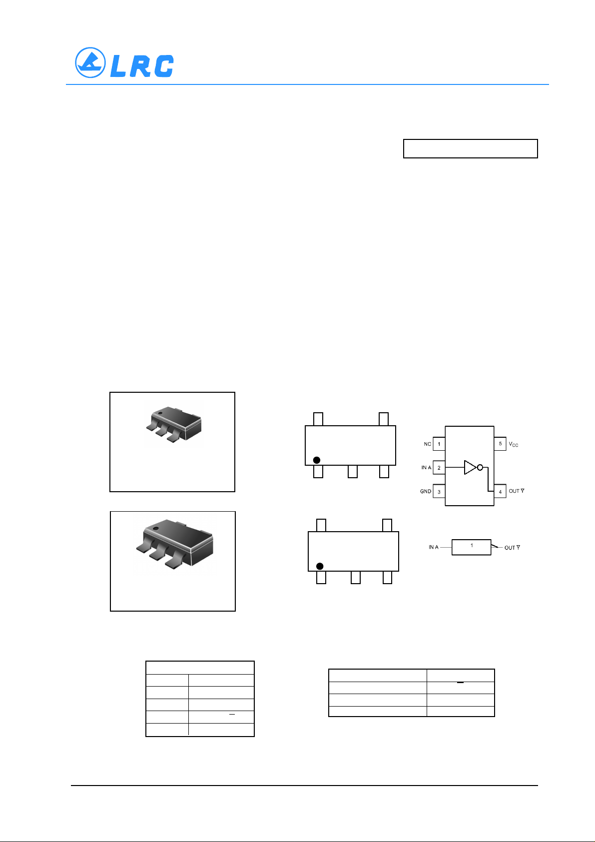
PIN ASSIGNMENT
• Power Down Protection Provided on Inputs and Outputs
MARKING DIAGRAMS
5
4
1
2
3
SC–70/SC–88A/SOT–353
DF SUFFIX
CASE 419A
5
4
Pin 1
d = Date Code
VK
d
Figure 1. Pinout (Top View)
1
2
3
SOT–23/TSOP–5/SC–59
DT SUFFIX
CASE 483
PIN ASSIGNMENT
1NC
2 IN A
3 GND
4 OUT Y
5V
d
VK
Figure 2. Logic Symbol
Pin 1
d = Date Code
FUNCTION T ABLE
Inputs Output
AY
LH
HL
CC
ORDERING INFORMA TION
See detailed ordering and shipping information in the
package dimensions section on page 4 of this data sheet.
VHT4–1/4

LESHAN RADIO COMPANY, LTD.
MC74VHC1GT04
MAXIMUM RATINGS
Symbol Parameter Value Unit
V
CC
V
IN
V
OUT
I
IK
I
OK
I
OUT
I
CC
P
D
θ
JA
T
L
T
J
T stg Storage temperature –65 to +150 °C
V
ESD
I
LATCH–UP
1. Maximum Ratings are those values beyond which damage to the device may occur. Exposure to these conditions or conditions
beyond those indicated may adversely affect device reliability . Functional operation under absolute–maximum–rated conditions is
not implied. Functional operation should be restricted to the Recommended Operating Conditions.
2. Tested to EIA/JESD22–A114–A
3. Tested to EIA/JESD22–A115–A
4. Tested to JESD22–C101–A
5. Tested to EIA/JESD78
DC Supply Voltage – 0.5 to + 7.0 V
DC Input Voltage – 0.5 to 7.0 V
DC Output Voltage V CC=0 – 0.5 to 7.0 V
High or Low State –0.5 to V cc + 0.5
Input Diode Current –20 mA
Output Diode Current V
< GND; V
OUT
OUT
> V
CC
+20 mA
DC Output Current, per Pin + 25 mA
DC Supply Current, V
and GND +50 mA
CC
Power dissipation in still air SC–88A, TSOP–5 200 mW
Thermal resistance SC–88A, TSOP–5 333 °C/W
Lead Temperature, 1 mm from Case for 10 s 260 °C
Junction T emperature Under Bias + 150 °C
ESD Withstand Voltage Human Body Model (Note 2) >2000 V
Machine Model (Note 3) > 200
Charged Device Model (Note 4) N/A
Latch–Up Performance Above V
and Below GND at 125°C (Note 5) ± 500 mA
CC
RECOMMENDED OPERATING CONDITIONS
Symbol Parameter Min Max Unit
V
V
V
T
t r ,t
CC
IN
OUT
A
f
DC Supply Voltage 3.0 5.5 V
DC Input Voltage 0.0 5.5 V
DC Output Voltage V
High Low State 0.0 V
= 0 0.0 5.5 V
CC
CC
Operating T emperature Range – 55 + 125 °C
Input Rise and Fall Time V
= 3.3 ± 0.3 V 0 100 ns/V
CC
V
= 5.0 ± 0.5 V 0 20
CC
DEVICE JUNCTION TEMPERATURE VERSUS
TIME TO 0.1% BOND FAILURES
Junction Time, Time,
Temperature °C Hours Years
80 1,032,200 117.8
90 419,300 47.9
100 178,700 20.4
110 79,600 9.4
1
120 37,000 4.2
130 17,800 2.0
NORMALIZED FAILURE RATE
1 1 0 100 1000
140 8,900 1.0
TIME, YEARS
Figure 3. Failure Rate vs. Time Junction Temperature
VHT4–2/4
 Loading...