

Datasheet MC74VHC1G01DFT1, MC74VHC1G01DFT2, MC74VHC1G01DTT1, MC74VHC1G01DTT3, MC74VHC1G01DFT4 Datasheet (LRC)
2–Input NAND Gate with
LESHAN RADIO COMPANY, LTD.
Open Drain Output
The MC74VHC1G01 is an advanced high speed CMOS 2–input NAND gate with an open drain output fabricated with silicon gate
CMOS technology. It achieves high speed peration similar to equivalent Bipolar Schottky TTL while maintaining CMOS low power dissipation.
The internal circuit is composed of three stages, including an open drain output which provides the ability to set output switching level.
This allows the MC74VHC1G01 to be used to interface 5 V circuits to circuits of any voltage between V
resistor and power supply.
The MC74VHC1G01 input structure provides protection when voltages up to 7 V are applied, regardless of the supply voltage.
• High Speed: t
• Low Internal Power Dissipation: I
• Power Down Protection Provided on Inputs
• Pin and Function Compatible with Other Standard Logic Families
• Chip Complexity: FETs = 62; Equivalent Gates = 16
= 3.7 ns (Typ) at V
PD
= 5 V
CC
= 2 mA (Max) at T A = 25°C
CC
MC74VHC1G01
and 7 V using an external
CC
MARKING DIAGRAMS
5
4
1
2
3
SC–88A / SOT–353/SC–70
DF SUFFIX
CASE 419A
5
4
Pin 1
d = Date Code
V0
d
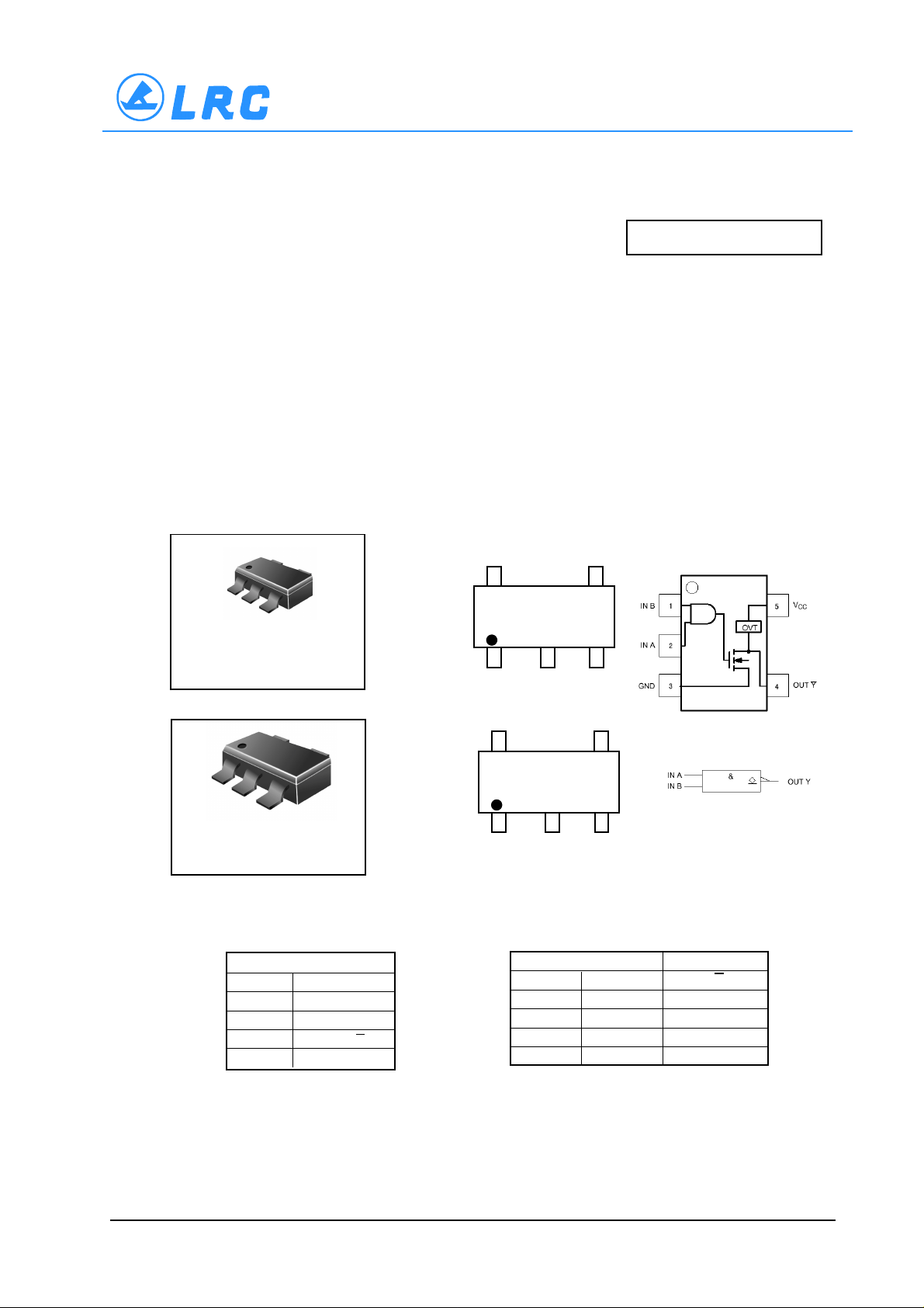
Figure 1. Pinout (Top View)
1
2
3
TSOP–5/SOT–23/SC–59
DT SUFFIX
CASE 483
PIN ASSIGNMENT
1 IN B
2 IN A
3 GND
4 OUT Y
5V
d
V0
Figure 2. Logic Symbol
Pin 1
d = Date Code
FUNCTION T ABLE
Inputs Output
AB Y
LL Z
LH Z
HL Z
CC
HH L
ORDERING INFORMATION
See detailed ordering and shipping information in the
package dimensions section on page 4 of this data sheet.
VH1–1/4
LESHAN RADIO COMPANY, LTD.
MC74VHC1G00
MAXIMUM RATINGS
Symbol Parameter Value Unit
V
CC
V
IN
V
OUT
I
IK
I
OK
I
OUT
I
CC
P
D
θ
JA
T
L
T
J
T
stg
V
ESD
I
LATCH–UP
1. Maximum Ratings are those values beyond which damage to the device may occur. Exposure to these conditions or conditions
beyond those indicated may adversely affect device reliability . Functional operation under absolute–maximum–rated conditions is
not implied. Functional operation should be restricted to the Recommended Operating Conditions.
2. Tested to EIA/JESD22–A114–A
3. Tested to EIA/JESD22–A115–A
4. Tested to JESD22–C101–A
5. Tested to EIA/JESD78
RECOMMENDED OPERATING CONDITIONS
Symbol Parameter Min Max Unit
V
CC
V
IN
V
OUT
T
A
t r ,t
f
DC Supply Voltage – 0.5 to + 7.0 V
DC Input Voltage – 0.5 to 7.0 V
DC Output V oltage – 0.5 to 7.0 V
DC Input Diode Current –20 mA
DC Output Diode Current V
< GND; V
OUT
OUT
> V
CC
+20 mA
DC Output Sink Current + 25 mA
DC Supply Current per Supply Pin +50 mA
Power dissipation in still air SC–88A, TSOP–5 200 mW
Thermal resistance SC–88A, TSOP–5 333 °C/W
Lead Temperature, 1 mm from Case for 10 Seconds 260 °C
Junction T emperature Under Bias + 150 °C
Storage temperature –65 to +150 °C
ESD Withstand Voltage Human Body Model (Note 2) >2000 V
Machine Model (Note 3) > 200
Charged Device Model (Note 4) N/A
Latch–Up Performance Above V
and Below GND at 125°C (Note 5) ± 500 mA
CC
DC Supply Voltage 2.0 5.5 V
DC Input Voltage 0.0 5.5 V
DC Output Voltage 0.0 7.0 V
Operating T emperature Range – 55 + 125 °C
Input Rise and Fall Time V
= 3.3 ± 0.3 V 0 100 ns/V
CC
V
= 5.0 ± 0.5 V 0 20
CC
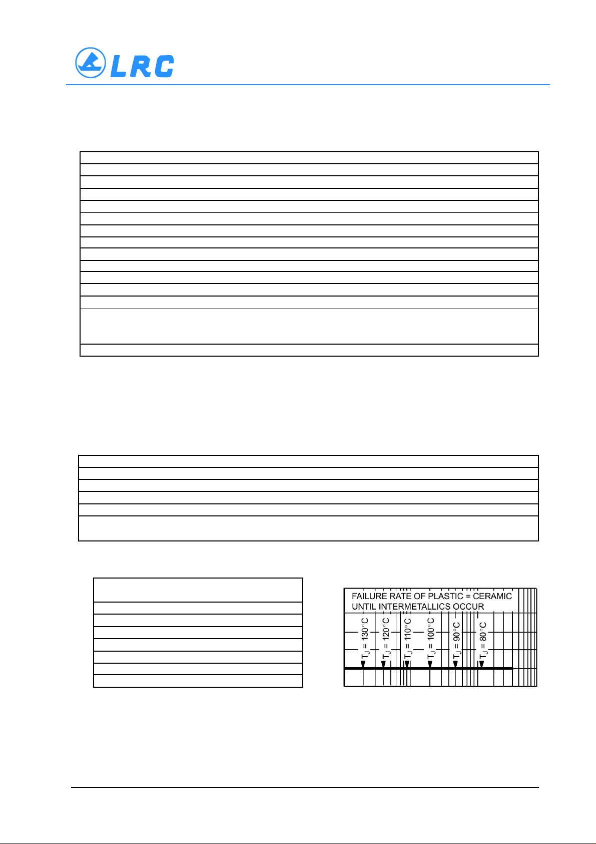
DEVICE JUNCTION TEMPERATURE VERSUS
TIME TO 0.1% BOND FAILURES
Junction Time, Time,
Temperature °C Hours Y ears
80 1,032,200 117.8
90 419,300 47.9
100 178,700 20.4
1 10 79,600 9.4
120 37,000 4.2
130 17,800 2.0
140 8,900 1.0
1
NORMALIZED FAILURE RATE
1 10 100 1000
TIME, YEARS
Figure 3. Failure Rate vs. Time
Junction Temperature
VH1–2/4

LESHAN RADIO COMPANY, LTD.
MC74VHC1G01
DC ELECTRICAL CHARACTERISTICS
V
CC
Symbol Parameter Test Conditions (V) Min Typ Max Min Max Min Max Unit
V
Minimum High–Level 2.0 1.5 1.5 1.5 V
IH
Input Voltage 3.0 2.1 2.1 2.1
4.5 3.15 3.15 3.15
5.5 3.85 3.85 3.85
V
Maximum Low–Level 2.0 0.5 0.5 0.5 V
IL
Input Voltage 3.0 0.9 0.9 0.9
4.5 1.35 1.35 1.35
5.5 1.65 1.65 1.65
V
V
I
Minimum High–Level V
OH
Output Voltage I
V
= V
or V
IN
IH
Maximum Low–Level
OL
Output Voltage I
V
= V
or V
IN
IH
Maximum Input
IN
= V
or V
IN
IH
IL
= – 50 µA 3.0 2.9 3.0 2.9 2.9
OH
IL
= V
V
I
OH
I
OH
V
OL
IL
V
I
OL
I
OL
V
IN
or V
IN
IH
IL
= –4 mA 3.0 2.58 2.48 2.34
= –8 mA 4.5 3.94 3.80 3.66
= V
or V
IN
IH
IL
= 50 µA 3.0 0.0 0.1 0.1 0.1
= V
or V
IN
IH
IL
= 4 mA 3.0 0.36 0.44 0.52
= 8 mA 4.5 0.36 0.44 0.52
= 5.5 V or GND 0 to5.5
2.0 1.9 2.0 1.9 1.9 V
4.5 4.4 4.0 4.4 4.4
2.0 0.0 0.1 0.1 0.1 V
4.5 0.0 0.1 0.1 0.1
Leakage Current
I
Maximum Quiescent
CC
V
= V
or GND 5.5 2.0 20 40
IN
CC
Supply Current
I OPD Maximum Off–state V OUT = 5.5 V 0 0.25 2.5 5.0 µA
Leakage Current
T A = 25°C T A <
±0.1 ±1.0 ±1.0 µA
85°C
–55°C to 125°C
µA
AC ELECTRICAL CHARACTERISTICS C
Symbol
Parameter Test Conditions Min Typ Max Min Max Min Max Unit
= 50 pF, Input t r = t f = 3.0 ns
load
T
= 25°C T A <
A
85°C
55°C to 125°C
t PZL Maximum Output V CC = 3.3 ± 0.3 V C L = 15 pF 5.5 7.9 9.5 11.0 ns
Enable Time, R L = R I = 500 Ω C L = 50 pF 8.0 1 1.4 13.0 15.5
Input A or B to Y
V CC = 5.0 ± 0.5 V C L = 15 pF 3.7 5.5 6.5 8.0
R L = R I = 500 Ω C L = 50 pF 5.2 7.5 8.5 8.0
t PLZ Maximum Output V CC = 3.3 ± 0.3 V C L = 50 pF 8.0 11.4 13.0 15.5 ns
Disable Time R L = R I = 500 Ω
V CC = 5.0 ± 0.5 V C L = 50 pF 5.2 7.5 8.5 10.0
R L = R I = 500 Ω
C IN Maximum Input 4 10 10 10 pF
Capacitance
Typical @ 25°C, V
C
PD
6. C
is defined as the value of the internal equivalent capacitance which is calculated from the operating current consumption without
PD
load. Average operating current can be obtained by the equation: I
load dynamic power consumption; P D = C
Power Dissipation Capacitance (Note 6) 18 pF
= C
x
V
x
f
2
x
V
x
f
CC
+ I
in
PD
CC(OPR)
x
V
CC
CC
PD
.
+ I
CC
in
= 5.0 V
CC
.
C
is used to determine the no–
CC
PD
VH1–3/4

LESHAN RADIO COMPANY, LTD.
MC74VHC1G01
Figure 4. Output V oltage Mismatch Application
Figure 6. Test Circuit
Figure 7. Complex Boolean Functions
Figure 5. Switching Waveforms
C L = 50 pF equivalent (Includes jig and probe capacitance)
R L = R 1 = 500 Ω or equivalent
R T = Z OUT of pulse generator (typically 50 Ω)
Figure 8. LED Driver
DEVICE ORDERING INFORMATION
Device Order
Number
MC74VHC1G01DFT1
MC74VHC1G01DFT2
MC74VHC1G01DFT4
MC74VHC1G01DTT1
MC74VHC1G01DTT3
Logic
Circuit
Indicator
MC 74 VHC1G 01 DF T1
MC 74 VHC1G 01 DF T2
MC 74 VHC1G 01 DF T4
MC 74 VHC1G 01 DT T1
MC 74 VHC1G 01 DT T3
T emp
Range
Identifier
Device Nomenclature
Technology
Device
Function
Figure 9. GTL Driver
Package
Suffix
Tape and
Reel Suffix
Package Type
(Name/SOT#/
Common Name)
SC–70/SC–88A/
SOT–353
SC–70/SC–88A/
SOT–353
SC–70/SC–88A/
SOT–353
SOT–23/TSOPS/
SC–59
SOT–23/TSOPS/
SC–59
Tape and
Reel Size
178 mm (7 in)
3000 Unit
178 mm (7 in)
3000 Unit
330 mm (13 in)
10,000 Unit
178 mm (7 in)
3000 Unit
330 mm (13 in)
10,000 Unit
VH1–4/4
 Loading...