

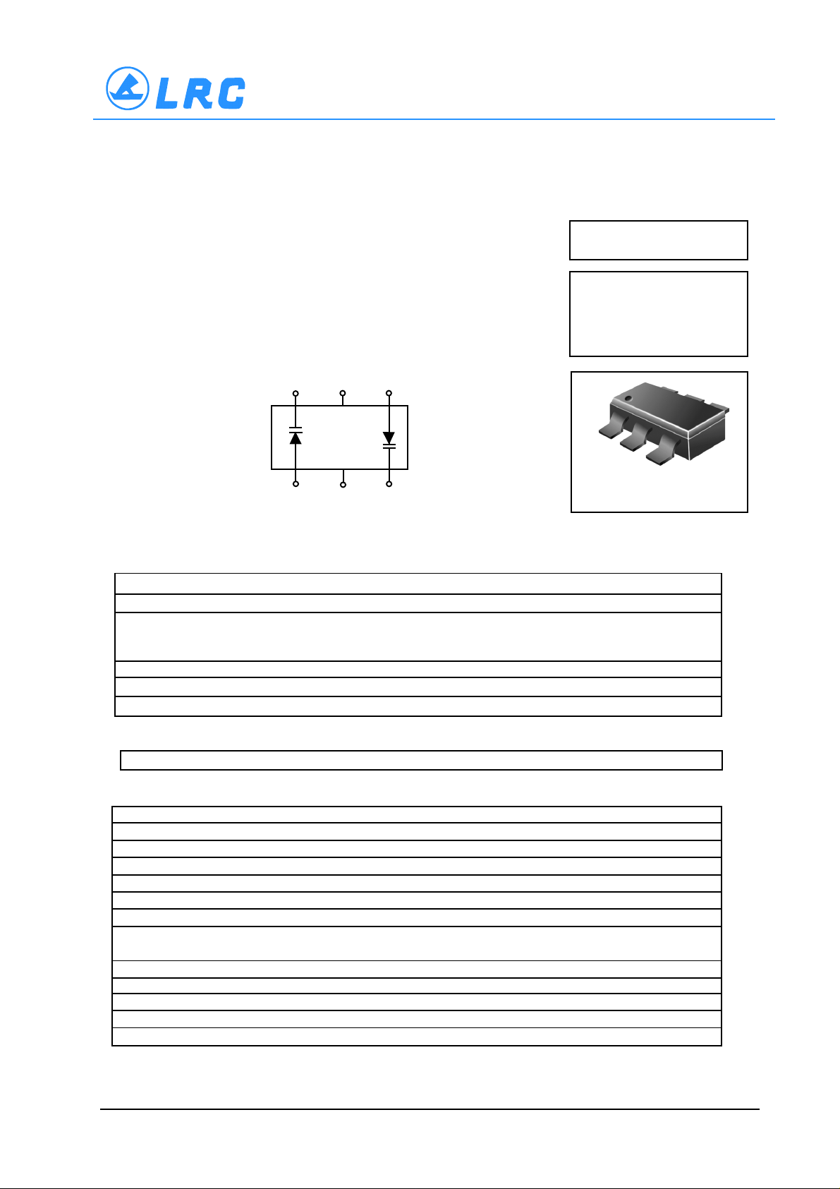
Dual SCHOTTKY Barrier Diodes
LESHAN RADIO COMPANY, LTD.
These SCHOTTKY barrier diodes are designed for high speed switching
MBD54DWT1
applications, circuit protection, and vol tage clamping. Extremely low forward
voltage reduces conduction loss. Miniature surface mount package is excellent
for hand held and portable applications where space is limited.
• Extremely Fast Switching Speed
• Low Forward Voltage — 0.35 V @ I F = 10 mAdc
DETECTOR AND SWITCHING
Cathode N/C Anode
654
1
123
Anode N/C Cathode
MAXIMUM RATINGS (T = 12 5°C unless otherwise noted)
Rating Symbol Value Unit
Reverse Voltage V R 30 Volts
Forward Power Dissipation P F
@ T A = 25°C 150 mW
Derate above 25°C 1.2 mW/°C
Forward Current (DC) I F 200 Max mA
Junction T emperature T J 125 Max °C
Storage Temperature Range T stg –55 to +150 °C
30 VOLTS
DUAL HOT–CARRIER
DIODES
6
5
2
3
SOT–363
CASE 419B–01, STYLE 6
4
DEVICE MARKING
MBD54DWT1 = BL
ELECTRICAL CHARACTERISTICS (T
Characteristic Symbol Min Typ Max Unit
Reverse Breakdown Voltage (I R = 10 µA) V
Total Capacitance (V R = 1.0 V , f = 1.0 MHz) C
Reverse Leakage (V R = 25 V) I
Forward Voltage (I F = 0.1 mAdc) V
Forward Voltage (I F = 30 mAdc) V
Forward Voltage (I F = 100 mAdc) V
Reverse Recovery Time
(I F = I R = 10 mAdc, I
Forward Voltage (I F = 1.0 mAdc) V
Forward Voltage (I F = 10 mAdc) V
Forward Current (DC) I
Repetitive Peak Forward Current I
Non–Repetitive Peak Forward Current (t <1.0s) I
= 1.0 mAdc) Figure 1
R(REC)
= 25°C unless otherwise noted) (EACH DIODE)
A
(BR)R
t
FRM
FSM
30 — — Volts
T
R
F
F
F
rr
F
F
F
— 7.6 10 pF
— 0.5 2.0 µAdc
— 0.22 0.24 Vdc
— 0.41 0.5 Vdc
— 0.52 1.0 Vdc
— — 5.0 ns
— 0.29 0.32 Vdc
— 0.35 0.40 Vdc
— — 200 mAdc
— — 300 mAdc
— — 600 mAdc
MBD54–1/4
LESHAN RADIO COMPANY, LTD.
MBD54DWT1
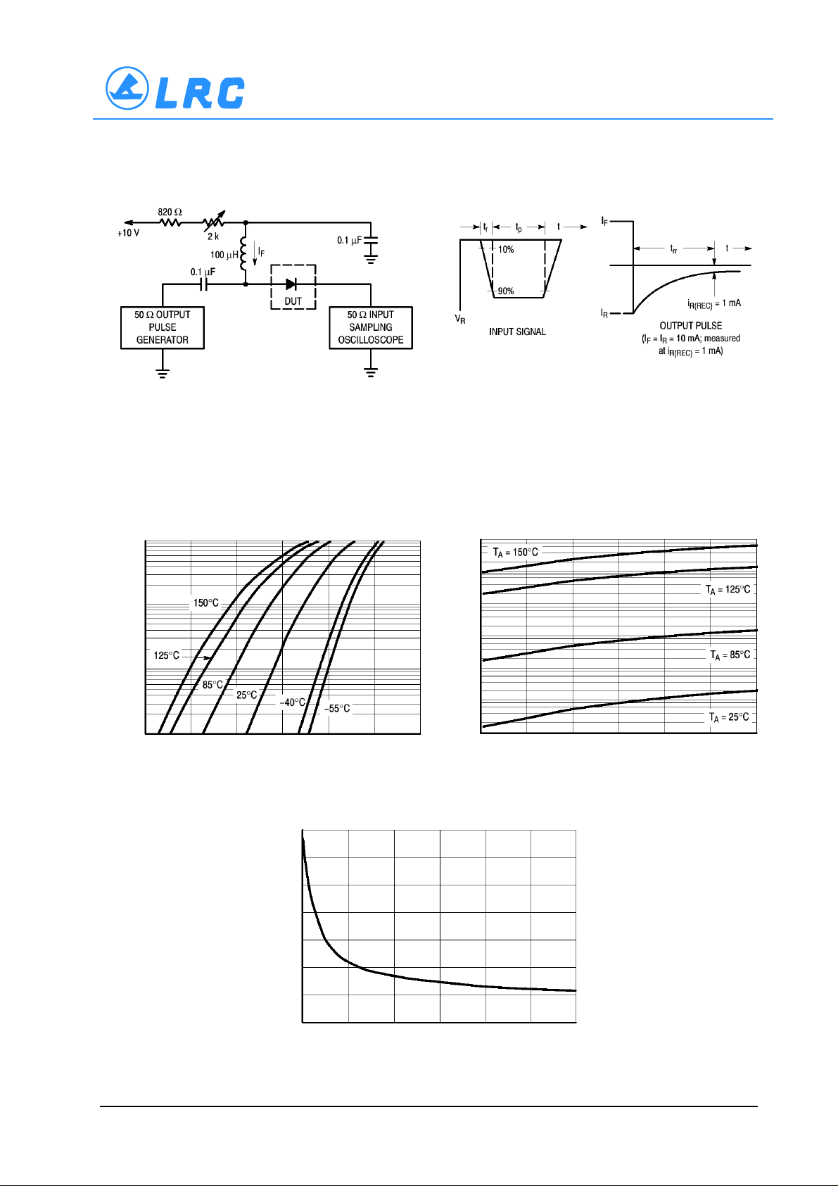
Notes: 1. A 2.0 kΩ variable resistor adjusted for a Forward Current (I F ) of 10 mA.
Notes: 2. Input pulse is adjusted so I R(peak) is equal to 10 mA.
Notes: 3. t p » t rr
Figure 1. Recovery Time Equivalent Test Circuit
100
10
1.0
, FORWARD CURRENT (mA)
F
I
0.1
0.0 0.1 0.2 0.3 0.4 0.5 0.6
V F , FORWARD VOLTAGE (VOLTS)
Figure 2. Forward Voltage
14
12
10
8
6
1000
100
10
1
0.1
0.01
, REVERSE CURRENT ( m A)
R
I
0.001
0 5 10 15 20 25 30
V R , REVERSE VOLTAGE (VOLTS)
Figure 3. Leakage Current
4
2
, TOT A L CAPACITANCE (pF)
T
C
0
0 5 10 15 20 25 30
V R , REVERSE VOLTAGE (VOLTS)
Figure 4. Total Capacitance
MBD54–2/4

LESHAN RADIO COMPANY, LTD.
MBD110DWT1 MBD330DWT1 MBD770DWT1
INFORMATION FOR USING THE SOT–363 SURF ACE MOUNT PACKAGE
MINIMUM RECOMMENDED FOOTPRINT FOR SURFACE MOUNTED APPLICATIONS
Surface mount board layout is a critical portion of the
total design. The footprint for the semiconductor packages
must be the correct size to insure proper solder connection
SOT–363
0.5 mm (min)
0.4 mm (min)
1.9 mm
SOT–363 POWER DISSIP ATION
The power dissipation of the SOT–363 is a function of
the pad size. This can vary from the minimum pad size for
soldering to a pad size given for maximum power dissipation.
Power dissipation for a surface mount device is determined
by TJ(max) , the maximum rated junction temperature of the
die, R qJA , the thermal resistance from the device junction
to ambient, and the operating temperature, T A . Using the
values provided on the data sheet for the SOT–363 package,
PD can be calculated as follows:
T
– T
J(max)
P D =
R
A
θJA
The values for the equation are found in the maximum
ratings table on the data sheet. Substituting these values
into the equation for an ambient temperature T A of 25°C,
one can calculate the power dissipation of the device which
in this case is 150 milliwatts.
150°C – 25°C
833°C/W
P D =
= 150 milliwatts
The 833°C/W for the SOT–363 package assumes the use
of the recommended footprint on a glass epoxy printed
circuit board to achieve a power dissipation of 150 milliwatts.
There are other alternatives to achieving higher power dissipation from the SOT–363 package. Another alternative
would be to use a ceramic substrate or
an aluminum core board such as Thermal CladE. Using a
board material such as Thermal Clad, an aluminum core
board, the power dissipation can be doubled using the same
footprint.
interface between the board and the package. With the
correct pad geometry, the packages will self align when
subjected to a solder reflow process.
0.65 mm 0.65 mm
SOLDERING PRECAUTIONS
The melting temperature of solder is higher than
the rated temperature of the device. When the entire
device is heated to a high temperature, failure to complete soldering within a short time could result in device failure. Therefore, the following items should always be observed in order to minimize the thermal stress
to which the devices are subjected.
• Always preheat the device.
• The delta temperature between the preheat and soldering should be 100°C or less.*
• When preheating and soldering, the temperature of
the leads and the case must not exceed the maximum
temperature ratings as shown on the data sheet. When
using infrared heating with the reflow soldering
method, the difference shall be a maximum of 10°C.
• The soldering temperature and time shall not exceed
260°C for more than 10 seconds.
• When shifting from preheating to soldering, the maximum temperature gradient shall be 5°C or less.
• After soldering has been completed, the device should
be allowed to cool naturally for at least three minutes.
Gradual cooling should be used as the use of forced
cooling will increase the temperature gradient and
result in latent failure due to mechanical stress.
• Mechanical stress or shock should not be applied during cooling.
* Soldering a device without preheating can cause ex-
cessive thermal shock and stress which can result in
damage to the device.
MBD54–3/4

LESHAN RADIO COMPANY, LTD.
MBD110DWT1 MBD330DWT1 MBD770DWT1
P ACKAGE DIMENSIONS
SC–88 (SOT–363)
CASE 419B–01
ISSUE G
A
G
V
5
6
S
1
H
4
B
3
2
D 6 PL
C
0.2 (0.008) M B M
N
K
NOTES:
1. DIMENSIONING AND TOLERANCING PER ANSI
Y14.5M, 1982.
2. CONTROLLING DIMENSION: INCH.
INCHES MILLIMETERS
DIM MIN MAX MIN M AX
A 0.071 0.087 1.80 2.20
B 0.045 0.053 1.15 1.35
C 0.031 0.043 0.80 1.10
D 0.004 0.012 0.10 0.30
G 0.026BSC 0.65BSC
H ––– 0.004 ––– 0.10
J 0.004 0.010 0.10 0.25
K 0.004 0.012 0.10 0.30
N 0.008 REF 0.20 REF
J
S 0.079 0.087 2.00 2.20
V 0.012 0.016 0.30 0.40
STYLE 1:
PIN 1. EMITTER 2
2. BASE 2
3. COLLECTOR 1
4. EMITTER 1
5. BASE 1
6. COLLECTOR 2
MBD54–4/4
 Loading...