

Page 1

LTM3210 Data Sheet
Shenzhen Longsys Technology Co., Ltd. www.Longsys.com
o Room 306-310, Building 4, Software Park 1, Nanshan District, Shenzhen, China
-1-
LTM3210 WIFI MODULE
Data Sheet
V1.8
Aug.2017
Page 2

LTM3210 Data Sheet
Shenzhen Longsys Technology Co., Ltd. www.Longsys.com
o Room 306-310, Building 4, Software Park 1, Nanshan District, Shenzhen, China
-2-
Revision
Date
Description
V1.0
2016/11/08
Initial release
V1.1
2017/01/18
Update pictures and manufacture
information
V1.2
2017/03/24
Add ordering information
V1.3
2017/04/18
Update Tcase 0-70°C
V1.4
2017/05/02
Update pinout definition
V1.5
2017/07/21
Add industrial spec
V1.6
2017/08/14
New add FCC Statement
V1.7
2017/08/15
Update the P11 output power table
V1.8
2017/08/23
Update the FCC Statement in P17 and new
add chip version notes in P16
Copyright
© 2016-2017 LONGSYS TECHNOLOGY CO., LTD.
This document is copyrighted with all rights reserved. No part of this publication may be reproduced,
transmitted, transcribed, stored in a retrieval system, or translated into any language in any form by any means
without the written permission of LONGSYS TECHNOLOGY CO., LTD.
Notice
LONGSYS TECHNOLOGY CO., LTD. reserves the right to change specifications without prior notice.
While the information in this manual has been compiled with great care, it may not be deemed an assurance of
product characteristics. LONGSYS TECHNOLOGY CO., LTD. shall be liable only to the degree specified in the
terms of sale and delivery.
The reproduction and distribution of the documentation and software supplied with this product and the use of
its contents is subject to written authorization from Shenzhen Longsys Technology Co.,Ltd..
Page 3

LTM3210 Data Sheet
Shenzhen Longsys Technology Co., Ltd. www.Longsys.com
o Room 306-310, Building 4, Software Park 1, Nanshan District, Shenzhen, China
-3-
1. Introduction ............................................................................................................... 4
2. Hardware Specification ............................................................................................ 6
2.1 LTM3210 module pinout ................................................................................................................................ 6
2.2 LTM3210 Interface summary ......................................................................................................................... 8
2.3 Bootstrap signals ............................................................................................................................................ 8
2.4 Electrical characteristics................................................................................................................................. 9
2.4.1 Absolute Maximum Ratings .......................................................................................................... 9
2.4.2 Recommended Operating Conditions ........................................................................................... 9
2.4.3 General DC electrical characteristics .......................................................................................... 10
2.4.4 LTM3210 radio Rx characteristics ............................................................................................... 10
2.4.5 LTM3210 radio Tx characteristics ................................................................................................ 11
2.5 Timing specifications ................................................................................................................................... 12
2.5.1 SPI master interface timing ......................................................................................................... 12
2.5.2 SPI slave interface timing ............................................................................................................ 13
3. Mechanical Interface Specification ....................................................................... 14
4. Manufacture information ....................................................................................... 15
4.1 Optical Inspection ........................................................................................................................................ 15
4.2 Rework ......................................................................................................................................................... 15
4.3 Handling ....................................................................................................................................................... 15
4.4 Soldering Recommendations ....................................................................................................................... 15
5. Ordering Information ............................................................................................. 16
6. FCC Statement ........................................................................................................ 17
Page 4
LTM3210 Data Sheet
Shenzhen Longsys Technology Co., Ltd. www.Longsys.com
o Room 306-310, Building 4, Software Park 1, Nanshan District, Shenzhen, China
-4-
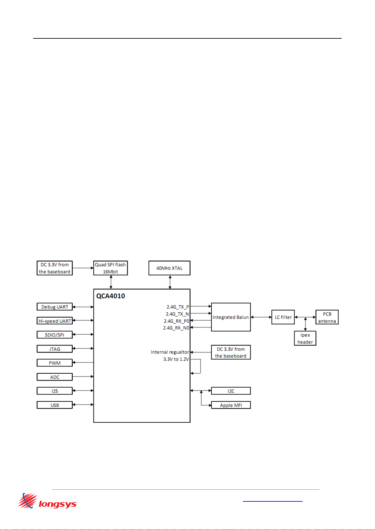
1. Introduction
LTM3210 Wi-Fi module provides a highly-integrated and flexible platform for developing and
evaluating products and applications based on the QCA4010 SoC.
LTM3210 module includes the following components:
■ QCA4010 chip
■ An integrated Balun to save cost and size, minimize tuning and tolerance
■ A printed antenna
■ Apple MFI (optional)
■ 2MB SPI Flash memory and etc.
The QCA4010 is a single band 1x1 802.11 b/g/n device optimized for low-power embedded
applications with single-stream capability for both Tx and Rx. It has an integrated network
processor with a large set of TCP/IP with IPv4/IPv6-based services. These services can be accessed
via a serial SPI link or by a UART link connected to an external host CPU.
Figure 1-1 LTM3210 block diagram
Page 5

LTM3210 Data Sheet
Shenzhen Longsys Technology Co., Ltd. www.Longsys.com
o Room 306-310, Building 4, Software Park 1, Nanshan District, Shenzhen, China
-5-
LTM3210 Wi-Fi link features
■ IEEE 802.11 b/g/n, single stream 1x1
■ Single-band 2.4 GHz
■ Integrated PA and LNA; support for external PA and external LNA
■ Green Tx power saving mode
■ Low power listen mode
■ Four-layer PCB design
■ Pre-certified FCC
■ Data rates up to 150 Mbps
■ Full security support: WPS,WEP, TKIP,WPA (personal),WPA2 (personal)
LTM3210 manufacturing interface
■ USB 2.0 interface with integrated controller and PHY for manufacturing test and configuration
LTM3210 host interfaces
■ UART host interface to a remote microcontroller with an AT style command set.
Page 6
LTM3210 Data Sheet
Shenzhen Longsys Technology Co., Ltd. www.Longsys.com
o Room 306-310, Building 4, Software Park 1, Nanshan District, Shenzhen, China
-6-
2. Hardware Specification
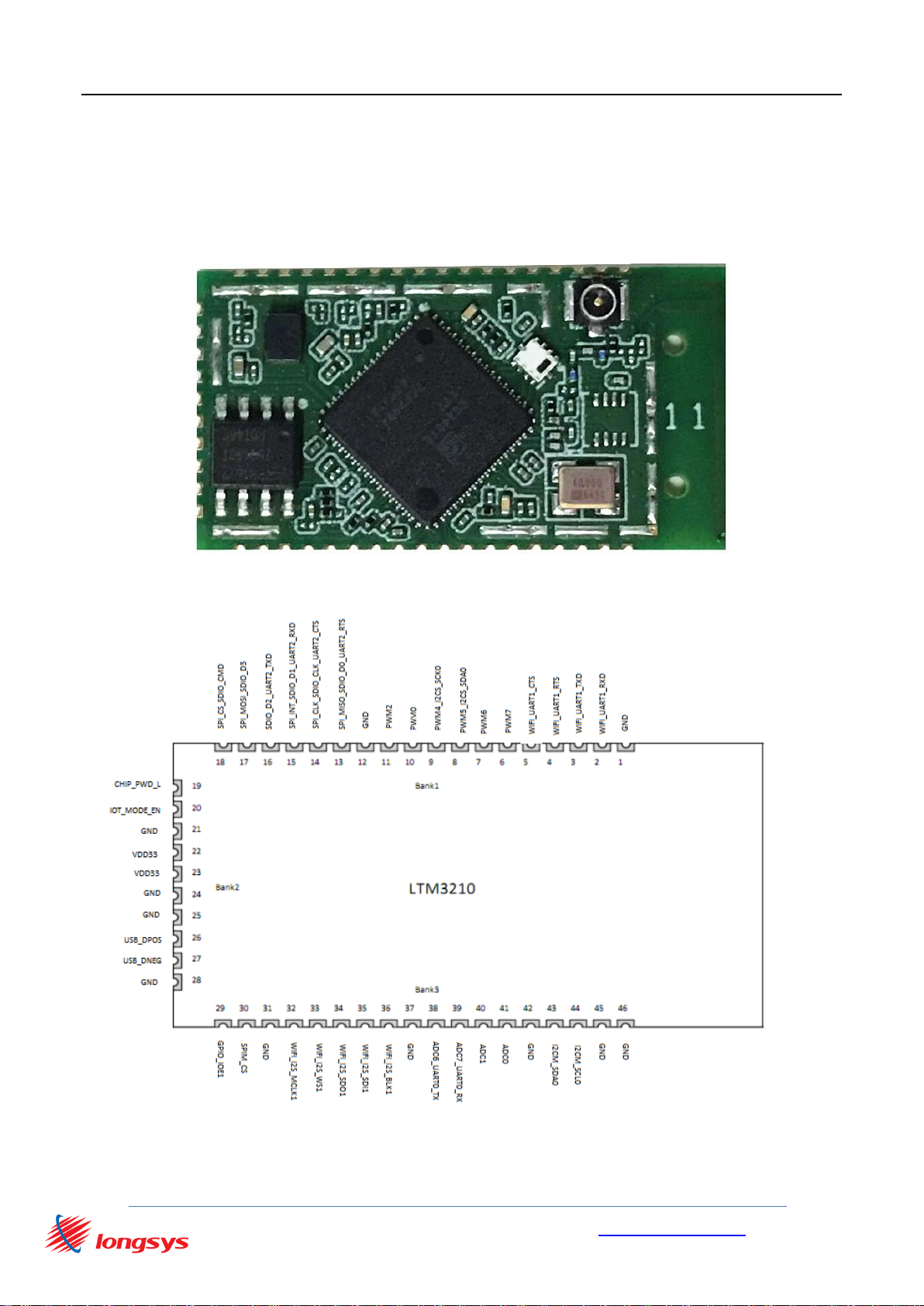
2.1 LTM3210 module pinout
Figure 2-1 LTM3210 top view
Figure 2-2 LTM3210 pinout definition
Page 7

LTM3210 Data Sheet
Shenzhen Longsys Technology Co., Ltd. www.Longsys.com
o Room 306-310, Building 4, Software Park 1, Nanshan District, Shenzhen, China
-7-
Table 2-1 LTM3210 module pinout definition and QCA4010 GPIO assignment
Pin
Signal/Interface
ALT1
ALT2
ALT3
GPIO No. 1 GND
Ground
- - -
2
WIFI_UART1_RXD
High speed UART RXD
-
-
GPIO[24] 3 WIFI_UART1_TXD
High speed UART TXD
-
-
GPIO[23] 4 WIFI_UART1_RTS
High speed UART RTS
-
-
GPIO[22] 5 WIFI_UART1_CTS
High speed UART CTS
-
-
GPIO[21] 6 PWM7
PWM7
-
-
GPIO[13] 7 PWM6
PWM6
-
-
GPIO[12]
8
PWM5_I2CS_SDA0
PWM5
I2C Slave
SDA0
-
GPIO[11] 9 PWM4_I2CS_SCK0
PWM4
I2C Slave
SCK0
-
GPIO[10]
10
PWM0
PWM0
-
-
GPIO[6]
11
PWM2
PWM2
-
-
GPIO[8]
12
GND
Ground
- - -
13
SPI_MISO_SDIO_D0_UART2_RTS
SPI MISO (master or slave)
SDIO Data0
UART RTS
GPIO[4]
14
SPI_CLK_SDIO_CLK_UART2_CTS
SPI CLK (master or slave)
SDIO CLK
UART CTS
GPIO[5]
15
SPI_INT_SDIO_D1_UART2_RXD
SPI Interrupt (slave)
SDIO Data1
UART RXD
GPIO[3]
16
SDIO_D2_UART2_TXD
-
SDIO Data2
UART TXD
GPIO[2]
17
SPI_MOSI_SDIO_D3
SPI MOSI (master or slave)
SDIO Data3
-
GPIO[1]
18
SPI_CS_SDIO_CMD
SPI CS (master or slave)
SDIO
Command
-
GPIO[0]
19
CHIP_PWD_L
Module reset, active low
- - -
20
IOT_MODE_EN
Wakeup manager enable
- - -
21
GND
Ground
- - -
22
VDD33
3.3V power supply
- - -
23
VDD33
3.3V power supply
- - -
24
GND
Ground
- - -
25
GND
Ground
- - -
26
USB_DPOS
USB Data+
- - -
27
USB_DNEG
USB Data-
- - -
28
GND
Ground
- - -
29
GPIO_IOE1
external wakeup
- - -
30
SPIM_CS
Flash memory /CS pin
-
-
GPIO[35]
31
GND
Ground
- - -
32
WIFI_I2S_MCLK1
I2S MCLK1
-
-
GPIO[33]
33
WIFI_I2S_WS1
I2S WS1
-
-
GPIO[32]
34
WIFI_I2S_SDO1
I2S SDO1
-
-
GPIO[31]
35
WIFI_I2S_SDI1
I2S SDI1
-
-
GPIO[30]
36
WIFI_I2S_BLK1
I2S BLK1
-
-
GPIO[27]
37
GND
Ground
- - -
Page 8

LTM3210 Data Sheet
Shenzhen Longsys Technology Co., Ltd. www.Longsys.com
o Room 306-310, Building 4, Software Park 1, Nanshan District, Shenzhen, China
-8-
38
ADC6_UART0_TX
ADC6
Debug UART
TXD
-
GPIO[29]
39
ADC7_UART0_RX
ADC7
Debug UART
RXD
-
GPIO[28]
40
ADC1
ADC1
- - -
41
ADC0
ADC0
- - -
42
GND
Ground
- - -
43
I2CM_SDA0
I2C Master SDA0
-
-
GPIO[25]
44
I2CM_SCL0
I2C Master SCL0
-
-
GPIO[26]
45
GND
Ground
- - -
46
GND
Ground
- - -
2.2 LTM3210 Interface summary
■ Host interface: SPI master x 1, SDIO2.0 x 1, debug UART x 1
■ High speed UART x 2
□ Up to 3Mbps data rate
■ I2C master x 1, I2C slave x 1
□ Standard-mode and fast-mode
■ I2S x 1
■ PWM x 6
□ 18-bit resolution with 8-bit clock prescaler
■ ADC x 4
□ 12-bit resolution, 400 Ksps for multiple channels and 1 Msps for single channel.
■ All signal pins can be multiplexed as GPIO
■ USB2.0 x 1, for ART tool
2.3 Bootstrap signals
Table 2-3 Bootstrap signals
Pin NO.
Bootstrap name
Description
11
Test mode enable
Should be low while reset released, for normal function
18
13
Host mode[1]
Host mode[0]
Bootstrap for host interface selection.
Default mode is 00.
00
USB/manufacturing test and configuration/hostless
01
Hostless (serial AT command) mode
10
SPI host mode
11
SDIO host mode
20
IOT mode enable
Keep high always, for normal function
Page 9

LTM3210 Data Sheet
Shenzhen Longsys Technology Co., Ltd. www.Longsys.com
o Room 306-310, Building 4, Software Park 1, Nanshan District, Shenzhen, China
-9-
2.4 Electrical characteristics
2.4.1 Absolute Maximum Ratings
Table 2-4-1 summarizes the absolute maximum ratings and Table 2-4-2 lists the recommended
operating conditions for the LTM3210. Absolute maximum ratings are those values beyond which
damage to the device can occur.
Functional operation under these conditions, or at any other condition beyond those indicated in the
operational sections of this document, is not recommended.
NOTE: Maximum rating for signals follows the supply domain of the signals.
Table 2-4-1 absolute maximum ratings
symbol
Description
Max rating
unit
VDD33
VDD supply for whole chip
–0.3 to 4.0
V
VIH MIN
Minimum Digital I/O Input Voltage for 1.8 V or 3.3 V I/O Supply
–0.3
V
3.3 V I/O VIH MAX
Maximum Digital I/O Input Voltage for 3.3 V I/O Supply
Vdd +0.3 V RFin
Maximum RF input (reference to 50-Ω input)
+10
dbm
Tstore
Storage Temperature
–45 to 135
°C
Tj
Junction Temperature
125
°C
ESD
Electrostatic Discharge Tolerance
HBM - 2000
CDM - 500
V
2.4.2 Recommended Operating Conditions
These conditions apply to all DC characteristics unless otherwise specified:
Tamb = 25 °C, Vdd33= 3.3 V
Table 2-4-2 Recommended Operating Conditions
Symbol
Parameter
Min
Typ
Max
unit
VDD33
VDD supply for whole chip
3.14
3.3
3.46
V
Operating Temperature Range
Commercial
0 - 70
°C
Operating Temperature Range
Industrial
-40 - 85
°C
Storage Temperature Range
-
-45 - 135
°C
Page 10

LTM3210 Data Sheet
Shenzhen Longsys Technology Co., Ltd. www.Longsys.com
o Room 306-310, Building 4, Software Park 1, Nanshan District, Shenzhen, China
-10-
2.4.3 General DC electrical characteristics
These conditions apply to all DC characteristics unless otherwise specified:
T
amb
= 25 °C, Vin = 3.3 V
Table 2-4-3 DC Electrical characteristics for digital I/Os
Symbol
Parameter
Min
Typ
Max
Unit
VIH
High level I voltage
1.8 - 3.6 V VIL
Low level I voltage
-0.3 - 0.3
V
VOH
High level O voltage
2.2 - 3.3
V
VOL
Low level O voltage
0 - 0.4
V
2.4.4 LTM3210 radio Rx characteristics
Table 2-4-4 LTM3210 Main Rx characteristics for 2.4Ghz operation
Symbol
Parameter
Conditions
Min
Typ
Max
Unit
Frx
RX input frequency range
-
2.412
-
2.462
GHz
Srf
Sensitivity
CCK
1Mbps
-
-93
-
dBm
11Mbps
-
-87
-
OFDM
6Mbps
-
-89
-
54Mbps
-
-73
-
HT20
MCS0
-
-89
-
MCS7
-
-70
-
Racj
Adjacent channel rejection
CCK
2Mbps
-
47
-
dB
OFDM
6Mbps
-
36
-
54Mbps
-
21
-
HT20
MCS0
-
34 - MCS7
-
18
-
In LPL mode, sensitivity will be degraded by 1~2dB.
Page 11

LTM3210 Data Sheet
Shenzhen Longsys Technology Co., Ltd. www.Longsys.com
o Room 306-310, Building 4, Software Park 1, Nanshan District, Shenzhen, China
-11-
2.4.5 LTM3210 radio Tx characteristics
Table 2-4-5 LTM3210 Tx characteristics for 2.4GHZ operation
Symbol
Parameter
Conditions
Min
Typ
Max
Unit
Ftx
Tx output frequency range
-
2.412
-
2.462
GHz
Pout
Output power
802.11b mask compliant
1 Mbps
-
18.53
-
dBm
802.11g mask compliant
6 Mbps
-
21.8
-
802.11g EVM compliant
54 Mbps
-
21.5
-
802.11n HT20 mask compliant
MCS0
-
19.73
-
802.11n HT20 EVM compliant
MCS7
-
19.4
-
Refer to IEEE802.11specification for TX spectrum limits:
802.11b mask(18.4.7.3)
802.11g mask(19.5.4)
802.11g EVM(17.3.9.6.3)
802.11n HT20 mask(20.3.21.1)
802.11n HT20 EVM(20.3.21.7.3)
Page 12

LTM3210 Data Sheet
Shenzhen Longsys Technology Co., Ltd. www.Longsys.com
o Room 306-310, Building 4, Software Park 1, Nanshan District, Shenzhen, China
-12-
2.5 Timing specifications
2.5.1 SPI master interface timing
Figure 2-3 LTM3210 SPI master timing
Table 2-5-1 SPI master timing
Parameter
Description
Min
Max
Unit
tCP
Clock period
30.7
1000
ns
tCSD
Chip select valid delay
-5.5 5 ns
tDD
Data valid delay
-5.5 5 ns
tDS
Data setup
3 - ns
tDH
Data hold
0 - ns
Page 13
LTM3210 Data Sheet
Shenzhen Longsys Technology Co., Ltd. www.Longsys.com
o Room 306-310, Building 4, Software Park 1, Nanshan District, Shenzhen, China
-13-
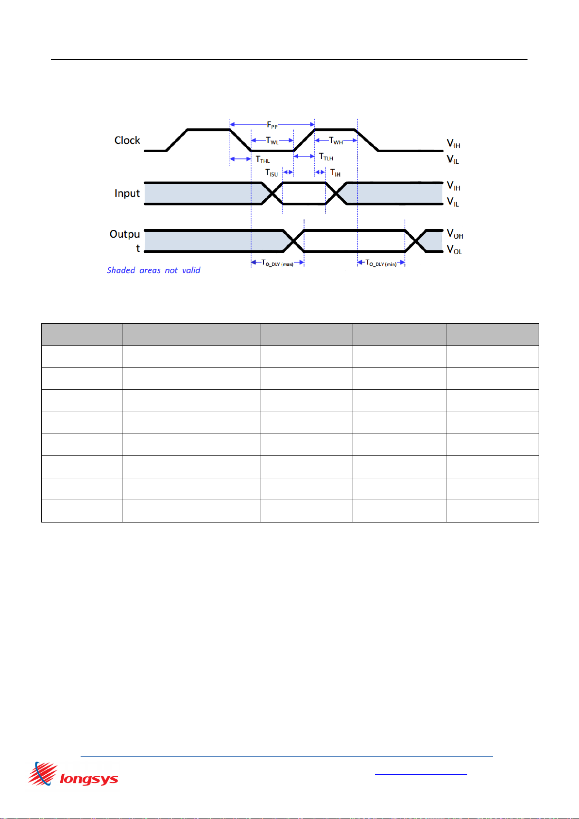
2.5.2 SPI slave interface timing
Figure 9-2 SPI Slave Timing
Table 2-5-2 SPI slave timing
Parameter
Description
Min
Max
Unit
f
PP
Clock frequency
0
48
MHz
t
WL
Clock low time
8.3 - ns
t
WH
Clock high time
8.33 - ns
t
TLH
Clock rise time
-
2
ns
t
THL
Clock fall time
-
2
ns
t
lSU
Input setup time
5 - ns
t
lH
Input hold time
5 - ns
t
O_DLY
Output delay
0 5 ns
Page 14
LTM3210 Data Sheet
Shenzhen Longsys Technology Co., Ltd. www.Longsys.com
o Room 306-310, Building 4, Software Park 1, Nanshan District, Shenzhen, China
-14-
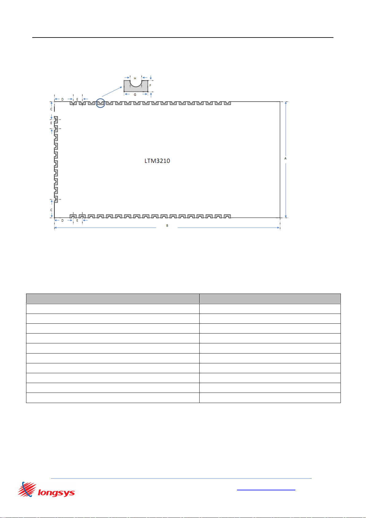
3. Mechanical Interface Specification
Figure 3-1 LTM3210 module dimensions
Table 3-1 LTM3210 module dimensions
Label
Dimension(mm)
A
16 B 30 C 2.285
D
2.54
E
1.27 F 0.4 G 0.7
H(diameter)
0.5
Module height(including the RF shield)
2.6
Total height (with a coax cable plugged into the U.FL connector)
3.6
Page 15

LTM3210 Data Sheet
Shenzhen Longsys Technology Co., Ltd. www.Longsys.com
o Room 306-310, Building 4, Software Park 1, Nanshan District, Shenzhen, China
-15-
4. Manufacture information
4.1 Optical Inspection
After SMT, LTM3210 PCBA will be automatically sent to do AOI (Automatic Optic Inspection).
Longsys uses TR7500 to check every CHIP.
TR7500 features:
3CCD camera with 5 detectors
All pictures have the sense of 3D
Resolution: 10μm
TR7500 can detect blemishes during SMT to guarantee quality at the first step before IOE and fully functional
test.
4.2 Rework
The module can be unsoldered from the host board if the Moisture Sensitivity Level (MSL) requirements are
met as described in this data sheet. Never attempt a rework on the module itself, e.g. replacing individual
components. Such actions will terminate warranty coverage.
4.3 Handling
The LTM3210 contains a highly sensitive electronic circuitry. Handling without proper ESD protection may
destroy or damage the chip permanently.
4.4 Soldering Recommendations
The LTM3210 can be SMT on the board following the temperature curve graph :
Figure 4-1 LTM3210 Profile Proposal
Page 16

LTM3210 Data Sheet
Shenzhen Longsys Technology Co., Ltd. www.Longsys.com
o Room 306-310, Building 4, Software Park 1, Nanshan District, Shenzhen, China
-16-
5.Ordering Information
LTM3210 -V W X X XYYYY ZZ
Chip Code
Code
Description
A
QCA-4010-0-116BDRQFN-XX-00-0,1MB,C-TEMP,V1.0
B
QCA-4010-1-116BDRQFN-XX-00-0,1MB,E-TEMP,V1.0
C
QCA-4010-2-116BDRQFN-XX-00-0,1.5MB,C-TEMP,V1.0
D
QCA-4010-3-116BDRQFN-XX-00-0,1.5MB,E-TEMP,V1.0
E
QCA-4010-0-116BDRQFN-XX-01-0,1MB,C-TEMP,V1.1
F
QCA-4010-2-116BDRQFN-XX-01-0,1.5MB,C-TEMP,V1.1
Note: XX=CHIP package pattern
Flash Code
Code
Description
2
8M bits of FM
4
16M bits of FM
Hardware Version
Code
Description
0
V1.00
1
V1.01
2
V1.02
3
V1.03
Antenna Code
Code
Description
P
Built-in PCB antenna
I
IPex connector for external antenna
Notes: The chip is only different in the temperature range & flash size of different chip versions.
And different chip versions have no different on the RF performance of the product.
Chip code
Data code(Internal)
Flash code
Hardware version
Antenna code
Batch code(Internal)
Page 17

LTM3210 Data Sheet
Shenzhen Longsys Technology Co., Ltd. www.Longsys.com
o Room 306-310, Building 4, Software Park 1, Nanshan District, Shenzhen, China
-17-
6. FCC Statement
This device complies with Part 15 of the FCC Rules. Operation is subject to the following two conditions: (1) this
device may not cause harmful interference, and (2) this device must accept any interference received, including
interference that may cause undesired operation.
Warning: changes or modifications not expressly approved by the party responsible for compliance could void the
user’s authority to operate the equipment.
Please notice that if the FCC identification number is not visible when the module is installed inside another
device, then the outside of the device into which the module is installed must also display a label referring to the
enclosed module. This exterior label can use wording such as the following: “Contains FCC ID:2AISR-LTM3210” any
similar wording that expresses the same meaning may be used.
RF Exposure Information:
This equipment complies with FCC radiation exposure limits set forth for an uncontrolled environment. This
equipment should be installed and operated with a minimum distance of 20cm between the radiator & your body.
This transmitter must not be co-located or operating in conjunction with any other antenna or transmitter.
Installation Information:
The module is limited to OEM installation ONLY.
The OEM integrator is responsible for ensuring that the end-user has no manual instruction to remove or install
module.
The module is limited to installation in mobile application;
A separate approval is required for all other operating configurations, including portable configurations with
respect to Part 2.1093 and difference antenna configurations.
The OEM integrator is responsible for ensuring that the host product which is installed and operating with the
module is in compliant with Part 15B unintentional Radiator requirements, please note that for a Class B digital
device or peripheral, the instructions furnished the user manual of the end-user product shall include the
following or similar statement, placed in a prominent location in the text of the manual:
Note: This equipment has been tested and found to comply with the limits for a Class B digital device, pursuant to
part 15 of the FCC Rules. These limits are designed to provide reasonable protection against harmful interference
in a residential installation. This equipment generates, uses and can radiate radio frequency energy and, if not
installed and used in accordance with the instructions, may cause harmful interference to radio communications.
However, there is no guarantee that interference will not occur in a particular installation. If this equipment does
cause harmful interference to radio or television reception, which can be determined by turning the equipment
off and on, the user is encouraged to try to correct the interference by one or more of the following measures:
—Reorient or relocate the receiving antenna.
—Increase the separation between the equipment and receiver.
—Connect the equipment into an outlet on a circuit different from that to which the receiver is connected.
—Consult the dealer or an experienced radio/TV technician for help.
 Loading...