LOGIC LPR520JC22 Datasheet

DEVICES INCORPORATED
LPR520
4 x 16-bit Multilevel Pipeline Register
LPR520
DEVICES INCORPORATED
4 x 16-bit Multilevel Pipeline Register
FEATURES DESCRIPTION
❑❑
❑ Four 16-bit Registers
❑❑
❑❑
❑ Implements Double 2-Stage
❑❑
Pipeline or Single 4-Stage Pipeline
Register
❑❑
❑ Hold, Shift, and Load Instructions
❑❑
❑❑
❑ Separate Data In and Data Out Pins
❑❑
❑❑
❑ High-Speed, Low Power CMOS
❑❑
Technology
❑❑
❑ Three-State Outputs
❑❑
❑❑
❑ 44-pin PLCC, J-Lead
❑❑
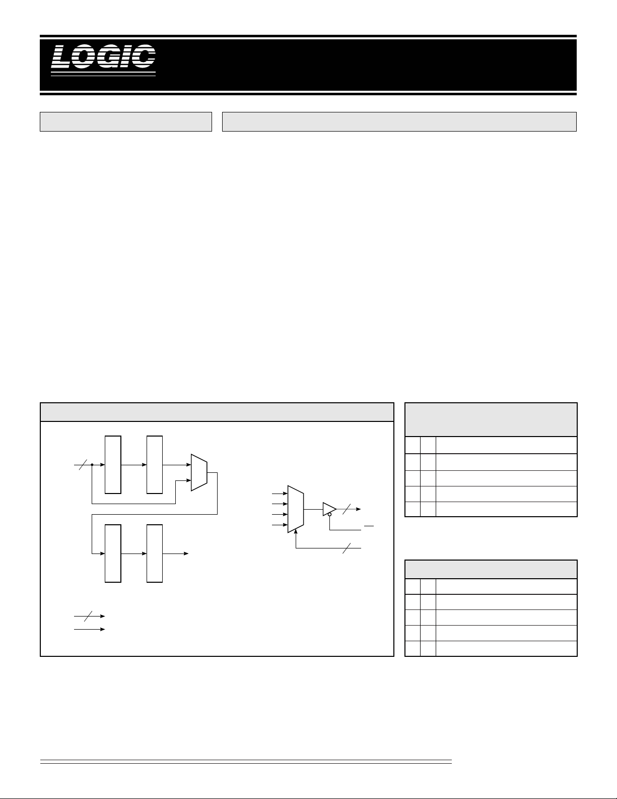
The LPR520 is functionally compatible with the L29C520 but have 16-bit
inputs and outputs. The LPR520 is
implemented in low power CMOS.
The LPR520 contains four registers
which can be configured as two
independent, 2-level pipelines or as
one 4-level pipeline.
The Instruction pins, I1-0, control the
loading of the registers. The registers
may be configured as a four-stage
delay line, with data loaded into R1
and shifted sequentially through R2,
R3, and R4. Also, data may be loaded
from the inputs into either R1 or R3
with only R2 or R4 shifting. Finally,
I1-0 may be set to prevent any register
from changing.
The S1-0 select lines control a 4-to-1
multiplexer which routes the contents
of any of the registers to the Y output
pins. The independence of the I and S
controls allows simultaneous write
and read operations on different
registers.
LPR520 BLOCK DIAGRAM
16
D15-0
I1-0
CLK
REGISTER 1
REGISTER 3
2
REGISTER 2
REGISTER 4
MUX
REG 1
REG 2
REG 3
REG 4
MUX
TABLE 1.
LPR520 INSTRUCTION TABLE
I1 I0 Description
LLD➞R1 R1➞R2 R2➞R3 R3➞R4
L H HOLD HOLD D➞R3 R3➞R4
16
15-0
Y
OE
2
S1-0
HLD➞R1 R1➞R2 HOLD HOLD
H H ALL REGISTERS ON HOLD
TABLE 2. OUTPUT SELECT
S1 S0 Register Selected
L L Register 4
L H Register 3
H L Register 2
H H Register 1
Pipeline Registers
1
08/02/2000–LDS.P520-C

DEVICES INCORPORATED
LPR520
4 x 16-bit Multilevel Pipeline Register
MAXIMUM RATINGS
Storage temperature ........................................................................................................... –65°C to +150°C
Operating ambient temperature........................................................................................... –55°C to +125°C
VCC supply voltage with respect to ground............................................................................ –0.5 V to +7.0V
Input signal with respect to ground ........................................................................................ –3.0 V to +7.0 V
Signal applied to high impedance output ............................................................................... –3.0 V to +7.0 V
Output current into low outputs............................................................................................................. 25 mA
Latchup current ............................................................................................................................... > 400 mA
OPERATING CONDITIONS
Active Operation, Commercial 0°C to +70°C 4.75 V ≤ VCC ≤ 5.25 V
Active Operation, Military –55°C to +125°C 4.50 V ≤ VCC ≤ 5.50 V
ELECTRICAL CHARACTERISTICS
Above which useful life may be impaired (Notes 1, 2, 3, 8)
To meet specified electrical and switching characteristics
Mode Temperature Range (Ambient) Supply Voltage
Over Operating Conditions (Note 4)
Symbol Parameter Test Condition Min Typ Max Unit
VOH Output High Voltage VCC = Min., IOH = –2.0 mA 2.4 V
VOL Output Low Voltage VCC = Min., IOL = 8.0 mA 0.5 V
VIH Input High Voltage 2.0 VCC V
V IL Input Low Voltage (Note 3) 0.0 0.8 V
IIX Input Current Ground ≤ VIN ≤ VCC (Note 12) ±20 µA
IOZ Output Leakage Current Ground ≤ VOUT ≤ VCC (Note 12) ±20 µA
ICC1 VCC Current, Dynamic (Notes 5, 6) 10 40 mA
ICC2 VCC Current, Quiescent (Note 7) 1.0 mA
Pipeline Registers
2
08/02/2000–LDS.P520-C
 Loading...