

DEVICES INCORPORATED
LMU08/8U
8 x 8-bit Parallel Multiplier
Multipliers
08/16/2000–LDS.08/8U-R
1
❑❑
❑❑
❑ 20 ns Worst-Case Multiply Time
❑❑
❑❑
❑ Low Power CMOS Technology
❑❑
❑❑
❑ LMU08 Replaces TRW TMC208K
❑❑
❑❑
❑ LMU8U Replaces TRW TMC28KU
❑❑
❑❑
❑ Two’s Complement (LMU08), or
Unsigned Operands (LMU8U)
❑❑
❑❑
❑ Three-State Outputs
❑❑
❑❑
❑ Package Styles Available:
• 40-pin PDIP
• 44-pin PLCC, J-Lead
FEATURES DESCRIPTION
LMU08/8U
8 x 8-bit Parallel Multiplier
DEVICES INCORPORATED
The LMU08 and LMU8U are high-
speed, low power 8-bit parallel
multipliers. They are pin-for-pin
equivalents with TRW TMC208K and
TMC28KU type multipliers. Full
military ambient temperature range
operation is attained by the use of
advanced CMOS technology.
Both the LMU08 and the LMU8U
produce the 16-bit product of two
8-bit numbers. The LMU08 accepts
operands in two’s complement format,
and produces a two’s complement
result. The product is provided in two
halves with the sign bit replicated as
the most significant bit of both halves.
This facilitates use of the LMU08
product as a double precision operand
in 8-bit systems. The LMU8U operates on unsigned data, producing an
unsigned magnitude result.
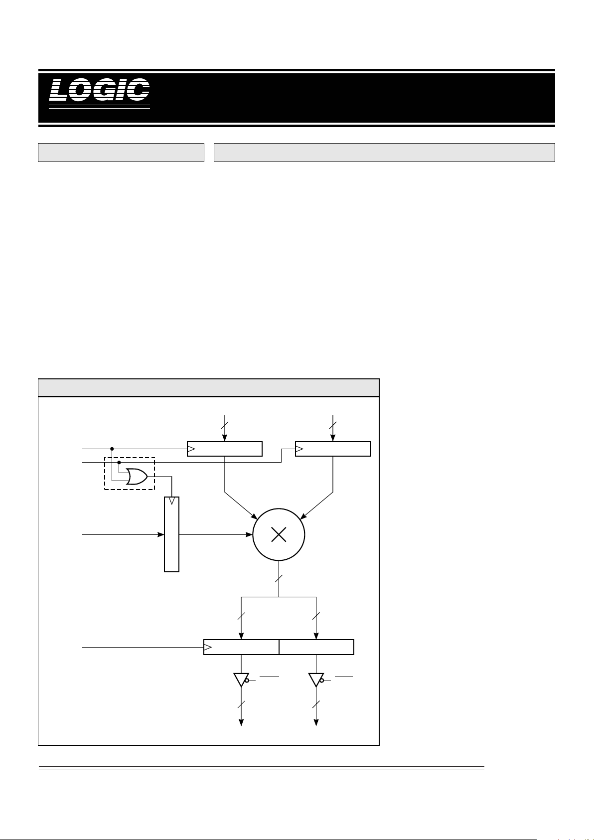
Both the LMU08 and the LMU8U
feature independently controlled
registers for both inputs and the
product, which along with three-state
outputs allows easy interfacing with
microprocessor busses. Provision is
made in the LMU08 and LMU8U for
proper rounding of the product to
8-bit precision. The round input is
loaded at the rising edge of the logical
OR of CLK A and CLK B for the
LMU08. The LMU8U latches RND on
the rising edge of CLK A only. In
either case, a ‘1’ is added in the most
significant position of the lower
product byte when RND is asserted.
Subsequent truncation of the least
significant product byte results in a
correctly rounded 8-bit result.
LMU08/8U BLOCK DIAGRAM
REGISTER
CLK A
CLK B
RND
CLK R
LMU08 Only
8
8
16
88
OEM
R
7-0
A
7-0
R
15-8
A REGISTER
B REGISTER
B
7-0
RESULT REGISTER
OEL
88
DEVICES INCORPORATED
LMU08/8U
8 x 8-bit Parallel Multiplier
Multipliers
08/16/2000–LDS.08/8U-R
2
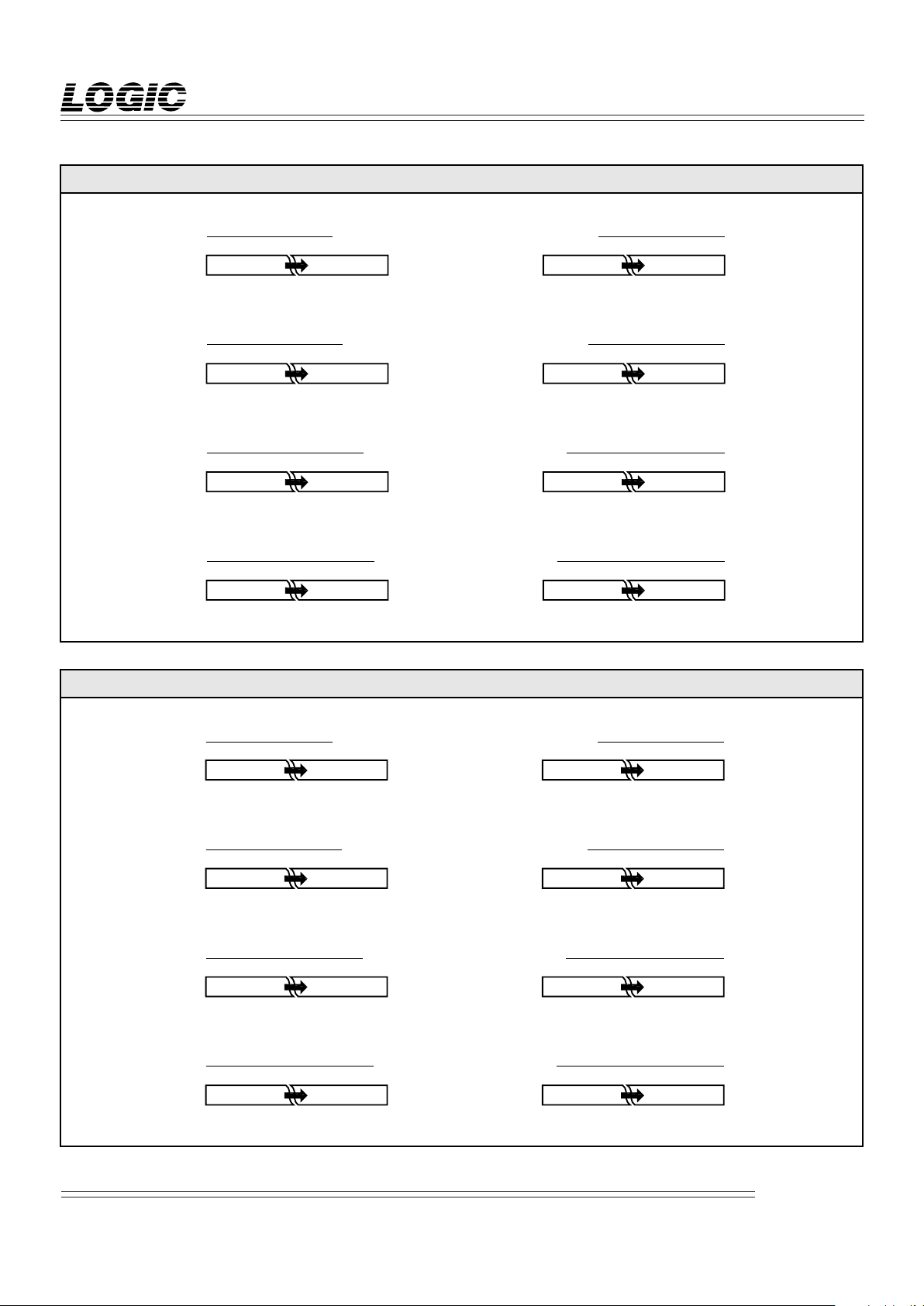
FIGURE 1A.INPUT FORMATS
FIGURE 1B.OUTPUT FORMATS
15 14 13 10 9 8
–2
0
(Sign)
2–12
–2
2–52–62
–7
765 210
–2
0
(Sign)
2–82
–9
2
–122–132–14
LMU08 Fractional Two’s Complement
15 14 13 10 9 8
–2
14
(Sign)
2132
12
29282
7
765 210
–2
14
(Sign)
262
5
22212
0
LMU08 Integer Two’s Complement
15 14 13 10 9 8
2
–12–22–3
2–62–72
–8
765 210
2
–92–102–11
2
–142–152–16
LMU8U Unsigned Fractional
15 14 13 10 9 8
2
15214213
210292
8
765 210
2
72625
22212
0
LMU8U Unsigned Integer
MSP LSP
765 210
–2
0
(Sign)
2–12
–2
2–52–62
–7
765 210
–2
0
(Sign)
2–12
–2
2–52–62
–7
LMU08 Fractional Two’s Complement
765 210
–2
7
(Sign)
262
5
22212
0
765 210
–2
7
(Sign)
262
5
22212
0
LMU08 Integer Two’s Complement
765 210
2
–12–22–3
2–62–72
–8
765 210
2
–12–22–3
2–62–72
–8
LMU8U Unsigned Fractional
765 210
2
72625
22212
0
765 210
2
72625
22212
0
LMU8U Unsigned Integer
A
IN
B
IN
DEVICES INCORPORATED
LMU08/8U
8 x 8-bit Parallel Multiplier
Multipliers
08/16/2000–LDS.08/8U-R
3
Storage temperature ........................................................................................................... –65°C to +150°C
Operating ambient temperature........................................................................................... –55°C to +125°C
VCC supply voltage with respect to ground............................................................................ –0.5 V to +7.0V
Input signal with respect to ground ........................................................................................ –3.0 V to +7.0 V
Signal applied to high impedance output ............................................................................... –3.0 V to +7.0 V
Output current into low outputs............................................................................................................. 25 mA
Latchup current ............................................................................................................................... > 400 mA
MAXIMUM RATINGS
Above which useful life may be impaired (Notes 1, 2, 3, 8)
OPERATING CONDITIONS
To meet specified electrical and switching characteristics
ELECTRICAL CHARACTERISTICS
Over Operating Conditions (Note 4)
Mode Temperature Range (Ambient) Supply Voltage
Active Operation, Commercial 0°C to +70°C 4.75 V ≤ VCC ≤ 5.25 V
Active Operation, Military –55°C to +125°C 4.50 V ≤ VCC ≤ 5.50V
Symbol Parameter Test Condition Min Typ Max Unit
VOH Output High Voltage VCC = Min., IOH = –2.0 mA 2.4 V
VOL Output Low Voltage VCC = Min., IOL = 8.0 mA 0.5 V
VIH Input High Voltage 2.0 VCC V
V IL Input Low Voltage (Note 3) 0.0 0.8 V
IIX Input Current Ground ≤ VIN ≤ VCC (Note 12) ±20 µA
IOZ Output Leakage Current Ground ≤ VOUT ≤ VCC (Note 12) ±20 µA
ICC1 VCC Current, Dynamic (Notes 5, 6) 824mA
ICC2 VCC Current, Quiescent (Note 7) 1.0 mA

DEVICES INCORPORATED
LMU08/8U
8 x 8-bit Parallel Multiplier
Multipliers
08/16/2000–LDS.08/8U-R
4
2345678901
2
2345678901
2
2345678901
2
2345678901
2
2345678901
2
2345678901
2
2345678901
2
2345678901
2
2345678901
2
2345678901
2
2345678901
2
2345678901
2
2345678901
2
2345678901
2
2345678901
2
2345678901
2
2345678901
2
2345678901
2
2345678901
2
2345678901
2
2345678901
2
2345678901
2
2345678901
2
2345678901
2
2345678901
2
2345678901
2
2345678901
2
2345678901
2
2345678901
2
2345678901
2
2345678901
2
2345678901
2
2345678901
2
2345678901
2
2345678901
2
2345678901
2
2345678901
2
2345678901
2
2345678901
2
2345678901
2
2345678901
2
2345678901
2
2345678901
2
2345678901
2
2345678901
2
2345678901
2
2345678901
2
2345678901
2
2345678901
2
2345678901
2
2345678901
2
2345678901
2
2345678901
2
2345678901
2
2345678901234567890123456789012123456789012
3
2345678901234567890123456789012123456789012
3
2345678901234567890123456789012123456789012
3
2345678901234567890123456789012123456789012
3
2345678901234567890123456789012123456789012
3
2345678901234567890123456789012123456789012
3
2345678901234567890123456789012123456789012
3
2345678901234567890123456789012123456789012
3
2345678901234567890123456789012123456789012
3
2345678901234567890123456789012123456789012
3
2345678901234567890123456789012123456789012
3
2345678901234567890123456789012123456789012
3
2345678901234567890123456789012123456789012
3
2345678901234567890123456789012123456789012
3
2345678901234567890123456789012123456789012
3
2345678901234567890123456789012123456789012
3
2345678901234567890123456789012123456789012
3
2345678901234567890123456789012123456789012
3
2345678901234567890123456789012123456789012
3
2345678901234567890123456789012123456789012
3
2345678901234567890123456789012123456789012
3
2345678901234567890123456789012123456789012
3
2345678901234567890123456789012123456789012
3
2345678901234567890123456789012123456789012
3
2345678901234567890123456789012123456789012
3
2345678901234567890123456789012123456789012
3
2345678901234567890123456789012123456789012
3
LMU08/8U–
90
*
60
*
45
*
25
*
Symbol Parameter Min Max Min Max Min Max Min Max
tMC Clocked Multiply Time 90 60 45 25
tPW Clock Pulse Width 25 20 15 10
tS Input Register Setup Time 20 15 15 15
tH Input Register Hold Time 5 2 2 2
tD Output Delay 35 22 22 20
tENA Three-State Output Enable Delay (Note 11) 35 24 24 20
tDIS Three-State Output Disable Delay (Note 11) 35 22 22 20
MILITARY OPERATING RANGE (–55°C to +125°C)
Notes 9, 10 (ns)
SWITCHING CHARACTERISTICS
LMU08/8U–
70
*
50 35 20
*
Symbol Parameter Min Max Min Max Min Max Min Max
tMC Clocked Multiply Time 70 50 35 20
tPW Clock Pulse Width 20 20 10 8
tS Input Register Setup Time 14 14 14 10
tH Input Register Hold Time 4 0 0 0
tD Output Delay 25 20 20 18
tENA Three-State Output Enable Delay (Note 11) 24 22 22 15
tDIS Three-State Output Disable Delay (Note 11) 22 20 20 15
COMMERCIAL OPERATING RANGE (0°C to +70°C)
Notes 9, 10 (ns)
2345678901234567890123
4
2345678901234567890123
4
*DISCONTINUED SPEED GRADE
SWITCHING WAVEFORMS
HIGH IMPEDANCE
INPUT
tENA
tDIS
tD
tPW
tMC
tPW
tHtS
CLK A
CLK B
CLK R
OEL
R
15-0
OEM

DEVICES INCORPORATED
LMU08/8U
8 x 8-bit Parallel Multiplier
Multipliers
08/16/2000–LDS.08/8U-R
5
1. Maximum Ratings indicate stress
specifications only. Functional operation of these products at values beyond
those indicated in the Operating Conditions table is not implied. Exposure to
maximum rating conditions for extended periods may affect reliability.
2. The products described by this specification include internal circuitry designed to protect the chip from damaging substrate injection currents and accumulations of static charge. Nevertheless, conventional precautions should
be observed during storage, handling,
and use of these circuits in order to
avoid exposure to excessive electrical
stress values.
3. This device provides hard clamping of
transient undershoot and overshoot. Input levels below ground or above VCC
will be clamped beginning at –0.6 V and
VCC + 0.6 V. The device can withstand
indefinite operation with inputs in the
range of –0.5 V to +7.0 V. Device operation will not be adversely affected, however, input current levels will be well in
excess of 100 mA.
4. Actual test conditions may vary from
those designated but operation is guaranteed as specified.
5. Supply current for a given application can be accurately approximated by:
where
N = total number of device outputs
C = capacitive load per output
V = supply voltage
F = clock frequency
6. Tested with all outputs changing every cycle and no load, at a 5 MHz clock
rate.
7. Tested with all inputs within 0.1 V of
VCC or Ground, no load.
8. These parameters are guaranteed
but not 100% tested.
NCV F
4
2
NOTES
9. AC specifications are tested with
input transition times less than 3 ns,
output reference levels of 1.5 V (except
tDIS test), and input levels of nominally
0 to 3.0 V. Output loading may be a
resistive divider which provides for
specified IOH and IOL at an output
voltage of VOH min and VOL max
respectively. Alternatively, a diode
bridge with upper and lower current
sources of IOH and IOL respectively,
and a balancing voltage of 1.5 V may be
used. Parasitic capacitance is 30 pF
minimum, and may be distributed.
This device has high-speed outputs capable of large instantaneous current
pulses and fast turn-on/turn-off times.
As a result, care must be exercised in the
testing of this device. The following
measures are recommended:
a. A 0.1 µF ceramic capacitor should be
installed between VCC and Ground
leads as close to the Device Under Test
(DUT) as possible. Similar capacitors
should be installed between device VCC
and the tester common, and device
ground and tester common.
b. Ground and VCC supply planes
must be brought directly to the DUT
socket or contactor fingers.
c. Input voltages should be adjusted to
compensate for inductive ground and VCC
noise to maintain required DUT input
levels relative to the DUT ground pin.
10. Each parameter is shown as a minimum or maximum value. Input requirements are specified from the point
of view of the external system driving
the chip. Setup time, for example, is
specified as a minimum since the external system must supply at least that
much time to meet the worst-case requirements of all parts. Responses from
the internal circuitry are specified from
the point of view of the device. Output
delay, for example, is specified as a
maximum since worst-case operation of
any device always provides data within
that time.
11. For the tENA test, the transition is
measured to the 1.5 V crossing point
with datasheet loads. For the tDIS test,
the transition is measured to the
±200mV level from the measured
steady-state output voltage with
±10mA loads. The balancing voltage, VTH, is set at 3.5 V for Z-to-0
and 0-to-Z tests, and set at 0 V for Zto-1 and 1-to-Z tests.
12. These parameters are only tested at
the high temperature extreme, which is
the worst case for leakage current.
S1
I
OH
I
OL
V
TH
C
L
DUT
OE
0.2 V
t
DIS
t
ENA
0.2 V
1.5 V 1.5 V
3.5V Vth
1
Z
0
Z
Z
1
Z
0
1.5 V
1.5 V
0V Vth
VOL*
V
OH
*
V
OL
*
V
OH
*
Measured V
OL
with IOH = –10mA and IOL = 10mA
Measured V
OH
with IOH = –10mA and IOL = 10mA
FIGURE B. THRESHOLD LEVELS
FIGURE A. OUTPUT LOADING CIRCUIT

DEVICES INCORPORATED
LMU08/8U
8 x 8-bit Parallel Multiplier
Multipliers
08/16/2000–LDS.08/8U-R
6
Plastic DIP
(P3)
LMU08PC35
40-pin — 0.6" wide
LMU08 — ORDERING INFORMATION
44-pin
0°C to +70°C — COMMERCIAL SCREENING
Plastic J-Lead
Chip Carrier (J1)
LMU08JC50
LMU08JC35
Speed
50 ns
35 ns
–55°C to +125°C — MIL-STD-883 COMPLIANT
–55°C to +125°C — COMMERCIAL SCREENING
1
2
3
4
5
6
7
8
9
10
11
12
13
14
15
16
17
18
19
20
40
39
38
37
36
35
34
33
32
31
30
29
28
27
26
25
24
23
22
21
R
10
R
9
R
8
CLK R
OEM
OEL
(R
7
) RSL
R
6
R
5
R
4
R
3
R
2
R
1
R
0
A
0
A
1
A
2
A
3
A
4
A
5
R
11
R
12
R
13
R
14
RSM (R15)
BS (B
7
)
B
6
B
5
GND
B
4
V
CC
B
3
B
2
B
1
B
0
RND
CLK B
CLK A
AS (A
7
)
A
6
41
7
8
9
10
11
12
13
14
15
16
17
39
38
37
36
35
34
33
32
31
30
29
44
Top
View
1 4243
18 23 24 25 26 27
406
28
2534
19 20 21 22
NC
BS (B
7
)
B
6
B
5
GND
B
4
V
CC
B
3
B
2
B
1
B
0
OEL
(R
7
) RSL
R
6
R
5
R
4
R
3
R
2
R
1
R
0
A
0
NC
NC
OEM
CLK R
R8R9R10R11R12R13R14RSM (R
15
)
A1A2A3A4A5A
6
(A
7
) AS
CLK A
CLK B
RND
NC

DEVICES INCORPORATED
LMU08/8U
8 x 8-bit Parallel Multiplier
Multipliers
08/16/2000–LDS.08/8U-R
7
Plastic DIP
(P3)
LMU8UPC50
LMU8UPC35
40-pin — 0.6" wide
LMU8U — ORDERING INFORMATION
44-pin
0°C to +70°C — COMMERCIAL SCREENING
Plastic J-Lead
Chip Carrier (J1)
LMU8UJC50
LMU8UJC35
Speed
50 ns
35 ns
–55°C to +125°C — MIL-STD-883 COMPLIANT
–55°C to +125°C — COMMERCIAL SCREENING
1
2
3
4
5
6
7
8
9
10
11
12
13
14
15
16
17
18
19
20
40
39
38
37
36
35
34
33
32
31
30
29
28
27
26
25
24
23
22
21
R10
R9
R8
CLK R
OEM
OEL
R
7
R6
R5
R4
R3
R2
R1
R0
A0
A1
A2
A3
A4
A5
R11
R12
R13
R14
R15
B7
B6
B5
GND
B
4
VCC
B3
B2
B1
B0
RND
CLK B
CLK A
A
7
A6
41
7
8
9
10
11
12
13
14
15
16
17
39
38
37
36
35
34
33
32
31
30
29
44
Top
View
1 4243
18 23 24 25 26 27
406
28
2534
19 20 21 22
NC
B
7
B
6
B
5
GND
B
4
V
CC
B
3
B
2
B
1
B
0
OEL
R
7
R
6
R
5
R
4
R
3
R
2
R
1
R
0
A
0
NC
NC
OEM
CLK R
R8R9R10R11R12R13R14R
15
A1A2A3A4A5A6A
7
CLK A
CLK B
RND
NC
 Loading...