LOGIC LMU217JC35, LMU217JC25 Datasheet

DEVICES INCORPORATED
LMU217
16 x 16-bit Parallel Multiplier
LMU217
DEVICES INCORPORATED
FEATURES DESCRIPTION
❑❑
❑ 25 ns Worst-Case Multiply Time
❑❑
❑❑
❑ Low Power CMOS Technology
❑❑
❑❑
❑ Replaces Cypress CY7C517,
❑❑
IDT 7217L, and AMD Am29517
❑❑
❑ Single Clock Architecture with
❑❑
Register Enables
❑❑
❑ Two’s Complement, Unsigned, or
❑❑
Mixed Operands
❑❑
❑ Three-State Outputs
❑❑
❑❑
❑ 68-pin PLCC, J-Lead
❑❑
The LMU217 is a high-speed, low
power 16-bit parallel multiplier.
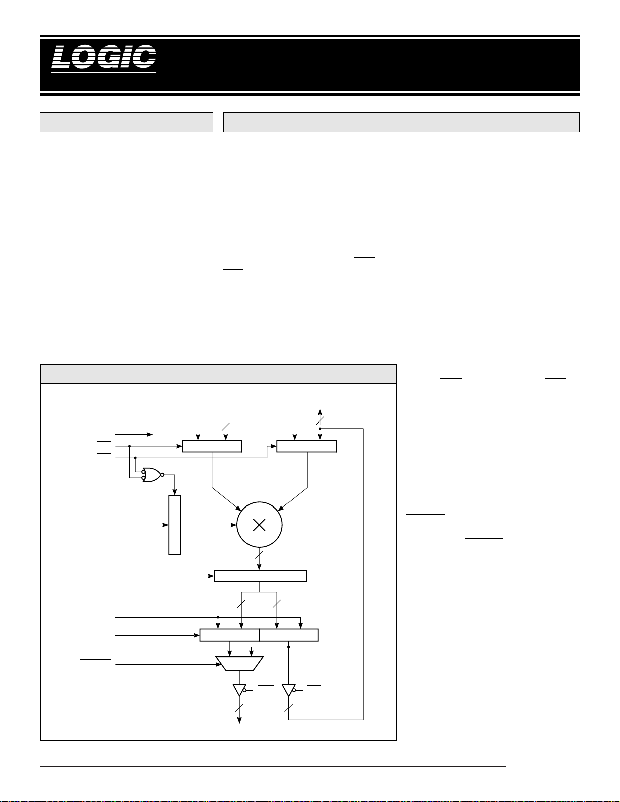
The LMU217 produces the 32-bit product of two 16-bit numbers. Data present
at the A inputs, along with the TCA
control bit, is loaded into the A register
on the rising edge of CLK. B data and
the TCB control bit are similarly
loaded. Loading of the A and B
registers is controlled by the ENA and
ENB controls. When HIGH, these controls prevent application of the clock to
the respective register. The TCA and
TCB controls specify the operands as
two’s complement when HIGH, or
unsigned magnitude when LOW.
LMU217 BLOCK DIAGRAM
A
15-0
16
CLK
ENA
ENB
TCA TCB
A REGISTER B REGISTER
16 x 16-bit Parallel multiplier
RND is loaded on the rising edge of
CLK, provided either ENA or ENB are
LOW. RND, when HIGH, adds ‘1’ to
the most significant bit position of the
least significant half of the product.
Subsequent truncation of the 16 least
significant bits produces a result
correctly rounded to 16-bit precision.
At the output, the Right Shift control
(RS) selects either of two output formats.
RS LOW produces a 31-bit product
with a copy of the sign bit inserted in the
MSB postion of the least significant half.
RS HIGH gives a full 32-bit product. Tw o
16-bit output registers are provided to
hold the most and least significant
halves of the result (MSP and LSP) as
defined by RS. These registers are
loaded on the rising edge of CLK, subject
B
15-0
/
R
15-0
16
to the ENR control. When ENR is
HIGH, clocking of the result registers is
prevented.
For asynchronous output, these registers
may be made transparent by setting the
feed through control (FT) HIGH and
ENR LOW.
RND
RS
FT
ENR
MSPSEL
REGISTER
32
FORMAT ADJUST
16 16
REGISTERRESULT
OEM OEL
16
R
31-16
16
The two halves of the product may be
routed to a single 16-bit three-state
output port (MSP) via a multiplexer.
MSPSEL LOW causes the MSP outputs
to be driven by the most significant half
of the result. MSPSEL HIGH routes the
least significant half of the result to the
MSP pins. In addition, the LSP is
available via the B port through a separate three-state buffer.
Multipliers
1
08/16/2000–LDS.217-H

DEVICES INCORPORATED
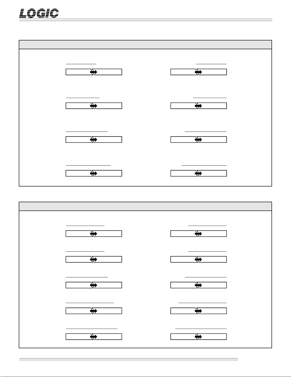
FIGURE 1A.INPUT FORMATS
LMU217
16 x 16-bit Parallel Multiplier
AIN BIN
Fractional Two’s Complement (TCA, TCB = 1)
15 14 13 2 1 0
0
–2
2–12
–2
(Sign)
15 14 13 2 1 0
–2
(Sign)
15
2142
13
15 14 13 2 1 0
–12–22–3
2
15 14 13 2 1 0
15214213
2
FIGURE 1B.OUTPUT FORMATS
–132–142–15
2
–2
(Sign)
0
2–12
Integer Two’s Complement (TCA, TCB = 1)
15 14 13 2 1 0
15 14 13 2 1 0
22212
0
–2
(Sign)
15
2142
Unsigned Fractional (TCA, TCB = 0)
15 14 13 2 1 0
–142–152–16
2
–12–22–3
2
Unsigned Integer (TCA, TCB = 0)
15 14 13 2 1 0
22212
0
15214213
2
–2
13
–132–142–15
2
22212
–142–152–16
2
22212
0
0
MSP LSP
Fractional Two’s Complement (RS = 0)
31 30 29 18 17 16
0
–2
(Sign)
2–12
–2
–132–142–15
2
Fractional Two’s Complement (RS = 1)
31 30 29 18 17 16
1
–2
(Sign)
202
–1
–122–132–14
2
Integer Two’s Complement (RS = 1)
31 30 29 18 17 16
–2
(Sign)
31
2302
29
2182172
31 30 29 18 17 16
–12–22–3
2
–142–152–16
2
31 30 29 18 17 16
2312302
29
2182172
15 14 13 2 1 0
–2
(Sign)
15 14 13 2 1 0
2
15 14 13 2 1 0
16
2152142
Unsigned Fractional (RS = 1)
15 14 13 2 1 0
2
Unsigned Integer (RS = 1)
15 14 13 2 1 0
16
2152142
0
–162–17
2
–152–162–17
–172–182–19
–282–292–30
2
–282–292–30
2
13
13
22212
–302–312–32
2
22212
0
0
Multipliers
2
08/16/2000–LDS.217-H
 Loading...