DEVICES INCORPORATED
LMU16/216
16 x 16-bit Parallel Multiplier
LMU16/216
DEVICES INCORPORATED
FEATURES DESCRIPTION
❑❑
❑ 20 ns Worst-Case Multiply Time
❑❑
❑❑
❑ Low Power CMOS Technology
❑❑
❑❑
❑ Replaces Fairchild MPY016/TMC216,
❑❑
Cypress CY7C516, IDT 7216L, and
AMD Am29516
❑❑
❑ Two’s Complement, Unsigned, or
❑❑
Mixed Operands
❑❑
❑ Three-State Outputs
❑❑
❑❑
❑ 68-pin PLCC, J-Lead
❑❑
The LMU16 and LMU216 are high-
speed, low power 16-bit parallel
multipliers. The LMU16 and
LMU216 are functionally identical;
they differ only in packaging.
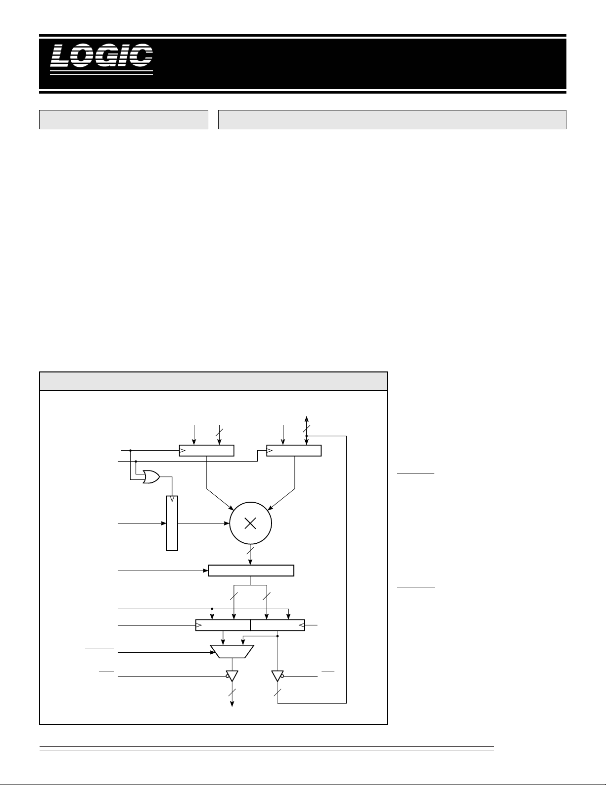
The LMU16 and LMU216 produce
the 32-bit product of two 16-bit
numbers. Data present at the A
inputs, along with the TCA control
bit, is loaded into the A register on
the rising edge of CLK A. B data
and the TCB control bit are
similarly loaded by CLK B. The
TCA and TCB controls specify the
A and B operands as two’s
complement when HIGH, or
unsigned magnitude when LOW.
LMU16/216 BLOCK DIAGRAM
A
15-0
16
32
FORMAT ADJUST
16 16
REGISTERRESULT
CLK A
CLK B
RND
RS
FT
CLK M
MSPSEL
TCA TCB
A REGISTER B REGISTER
REGISTER
16 x 16-bit Parallel Multiplier
RND is loaded on the rising edge of
the logical OR of CLK A and CLK B.
RND, when HIGH, adds ‘1’ to the
most significant bit position of the
least significant half of the product.
Subsequent truncation of the 16 least
significant bits produces a result
correctly rounded to 16-bit precision.
At the output, the Right Shift control
(RS) selects either of two output
formats. RS LOW produces a 31-bit
product with a copy of the sign bit
inserted in the MSB postion of the
least significant half. RS HIGH gives a
full 32-bit product. Two 16-bit output
registers are provided to hold the
most and least significant halves of the
result (MSP and LSP) as defined by
RS. These registers are loaded on the
rising edge of CLK M and CLK L
respectively. For asynchronous
B
15-0
/
R
15-0
16
CLK L
output, these registers may be made
transparent by setting the feed
through control (FT) HIGH.
The two halves of the product may be
routed to a single 16-bit three-state
output port (MSP) via a multiplexer.
MSPSEL LOW causes the MSP
outputs to be driven by the most
significant half of the result. MSPSEL
HIGH routes the least significant half
of the result to the MSP outputs. In
addition, the LSP is available via the B
port through a separate three-state
buffer.
The output multiplexer control
MSPSEL uses a pin which is a supply
ground in the Fairchild MPY016H/
TMC216H. When this control is LOW
(GND), the function is that of the
MPY016H/TMC216H, thus allowing
full compatibility.
OEM OEL
16
R
31-16
16
1
Multipliers
08/16/2000–LDS.16/216-N

DEVICES INCORPORATED
FIGURE 1A.INPUT FORMATS
LMU16/216
16 x 16-bit Parallel Multiplier
AIN BIN
Fractional Two’s Complement (TCA, TCB = 1)
15 14 13 2 1 0
0
–2
2–12
–2
(Sign)
15 14 13 2 1 0
–2
(Sign)
15
2142
13
15 14 13 2 1 0
–12–22–3
2
15 14 13 2 1 0
15214213
2
FIGURE 1B.OUTPUT FORMATS
–132–142–15
2
–2
(Sign)
0
2–12
Integer Two’s Complement (TCA, TCB = 1)
15 14 13 2 1 0
15 14 13 2 1 0
22212
0
–2
(Sign)
15
2142
Unsigned Fractional (TCA, TCB = 0)
15 14 13 2 1 0
–142–152–16
2
–12–22–3
2
Unsigned Integer (TCA, TCB = 0)
15 14 13 2 1 0
22212
0
15214213
2
–2
13
–132–142–15
2
22212
–142–152–16
2
22212
0
0
MSP LSP
Fractional Two’s Complement (RS = 0)
31 30 29 18 17 16
0
–2
(Sign)
2–12
–2
–132–142–15
2
Fractional Two’s Complement (RS = 1)
31 30 29 18 17 16
1
–2
(Sign)
202
–1
–122–132–14
2
Integer Two’s Complement (RS = 1)
31 30 29 18 17 16
–2
(Sign)
31
2302
29
2182172
31 30 29 18 17 16
–12–22–3
2
–142–152–16
2
31 30 29 18 17 16
2312302
29
2182172
15 14 13 2 1 0
–2
(Sign)
15 14 13 2 1 0
2
15 14 13 2 1 0
16
2152142
Unsigned Fractional (RS = 1)
15 14 13 2 1 0
2
Unsigned Integer (RS = 1)
15 14 13 2 1 0
16
2152142
0
–162–17
2
–152–162–17
–172–182–19
–282–292–30
2
–282–292–30
2
13
13
22212
–302–312–32
2
22212
0
0
Multipliers
2
08/16/2000–LDS.16/216-N

DEVICES INCORPORATED
LMU16/216
16 x 16-bit Parallel Multiplier
MAXIMUM RATINGS
Storage temperature ........................................................................................................... –65°C to +150°C
Operating ambient temperature........................................................................................... –55°C to +125°C
VCC supply voltage with respect to ground............................................................................ –0.5 V to +7.0V
Input signal with respect to ground ........................................................................................ –3.0 V to +7.0 V
Signal applied to high impedance output ............................................................................... –3.0 V to +7.0 V
Output current into low outputs............................................................................................................. 25 mA
Latchup current ............................................................................................................................... > 400 mA
OPERATING CONDITIONS
Active Operation, Commercial 0°C to +70°C 4.75 V ≤ VCC ≤ 5.25 V
Active Operation, Military –55°C to +125°C 4.50 V ≤ VCC ≤ 5.50 V
ELECTRICAL CHARACTERISTICS
Above which useful life may be impaired (Notes 1, 2, 3, 8)
To meet specified electrical and switching characteristics
Mode Temperature Range (Ambient) Supply Voltage
Over Operating Conditions (Note 4)
Symbol Parameter Test Condition Min Typ Max Unit
VOH Output High Voltage VCC = Min., IOH = –2.0 mA 2.4 V
VOL Output Low Voltage VCC = Min., IOL = 8.0 mA 0.5 V
VIH Input High Voltage 2.0 VCC V
V IL Input Low Voltage (Note 3) 0.0 0.8 V
IIX Input Current Ground ≤ VIN ≤ VCC (Note 12) ±20 µA
IOZ Output Leakage Current Ground ≤ VOUT ≤ VCC (Note 12) ±20 µA
ICC1 VCC Current, Dynamic (Notes 5, 6) 12 25 mA
ICC2 VCC Current, Quiescent (Note 7) 1.0 mA
Multipliers
3
08/16/2000–LDS.16/216-N
 Loading...