

DEVICES INCORPORATED
LMS12
12-bit Cascadable Multiplier-Summer
LMS12
DEVICES INCORPORATED
12-bit Cascadable Multiplier-Summer
FEATURES DESCRIPTION
❑❑
❑ 12 x 12-bit Multiplier with
❑❑
Pipelined 26-bit Output Summer
❑❑
❑ Summer has 26-bit Input Port Fully
❑❑
Independent from Multiplier
Inputs
❑❑
❑ Cascadable to Form Video Rate FIR
❑❑
Filter with 3-bit Headroom
❑❑
❑ A, B, and C Input Registers Sepa-
❑❑
rately Enabled for Maximum
Flexibility
❑❑
❑ 28 MHz Data Rate for FIR Filtering
❑❑
Applications
❑❑
❑ High Speed, Low Power CMOS
❑❑
Technology
❑❑
❑ 84-pin PLCC, J-Lead
❑❑
The LMS12 is a high-speed 12 x 12-bit
combinatorial multiplier integrated
with a 26-bit adder in a single 84-pin
package. It is an ideal building block
for the implementation of very highspeed FIR filters for video, RADAR,
and other similar applications. The
LMS12 implements the general form
(A•B) + C. As a result, it is also useful
in implementing polynomial approximations to transcendental functions.
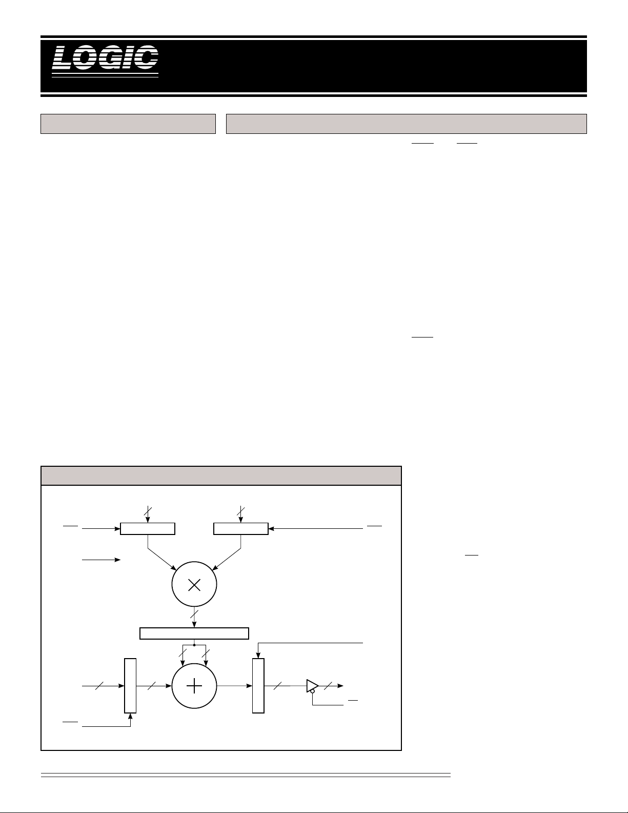
ARCHITECTURE
A block diagram of the LMS12 is
shown below. Its major features are
discussed individually in the following paragraphs.
MULTIPLIER
The A11-0 and B11-0 inputs to the
LMS12 are captured at the rising edge
of the clock in the 12-bit A and B input
registers, respectively. These registers
are independently enabled by the
LMS12 BLOCK DIAGRAM
A
11-0
12
ENA ENB
CLK
C
25-0
A REGISTER
24
PRODUCT REGISTER
SIGN
EXTENDED
26 26
26
C REGISTER
B
11-0
B REGISTER
242
12
26
S REGISTER
S
OE
25-0
FTS
ENA and ENB inputs. The registered
input data are then applied to a
12 x 12-bit multiplier array, which
produces a 24-bit result. Both the
inputs and outputs of the multiplier
are in two’s complement format. The
multiplication result forms the input
to the 24-bit product register.
SUMMER
The C25-0 inputs to the LMS12 form a
26-bit two’s complement number
which is captured in the C register at
the rising edge of the clock. The C
register is enabled by assertion of the
ENC input. The summer is a 26-bit
adder which operates on the C
register data and the sign extended
contents of the product register to
produce a 26-bit sum. This sum is
applied to the 26-bit S register.
OUTPUT
The FTS input is the feedthrough
control for the S register. When FTS is
asserted, the summer result is applied
directly to the S output port. When
FTS is deasserted, data from the S
register is output on the S port,
effecting a one-cycle delay of the
summer result. The S output port can
be forced to a high-impedance state by
driving the OE control line high. FTS
would be asserted for conventional
FIR filter applications, however the
insertion of zero-coefficient filter taps
may be accomplished by negating
FTS. Negating FTS also allows
application of the same filter transfer
function to two interleaved datastreams with successive input and
output sample points occurring on
alternate clock cycles.
ENC
Multiplier-Summers
1
08/16/2000–LDS.S12-J
DEVICES INCORPORATED
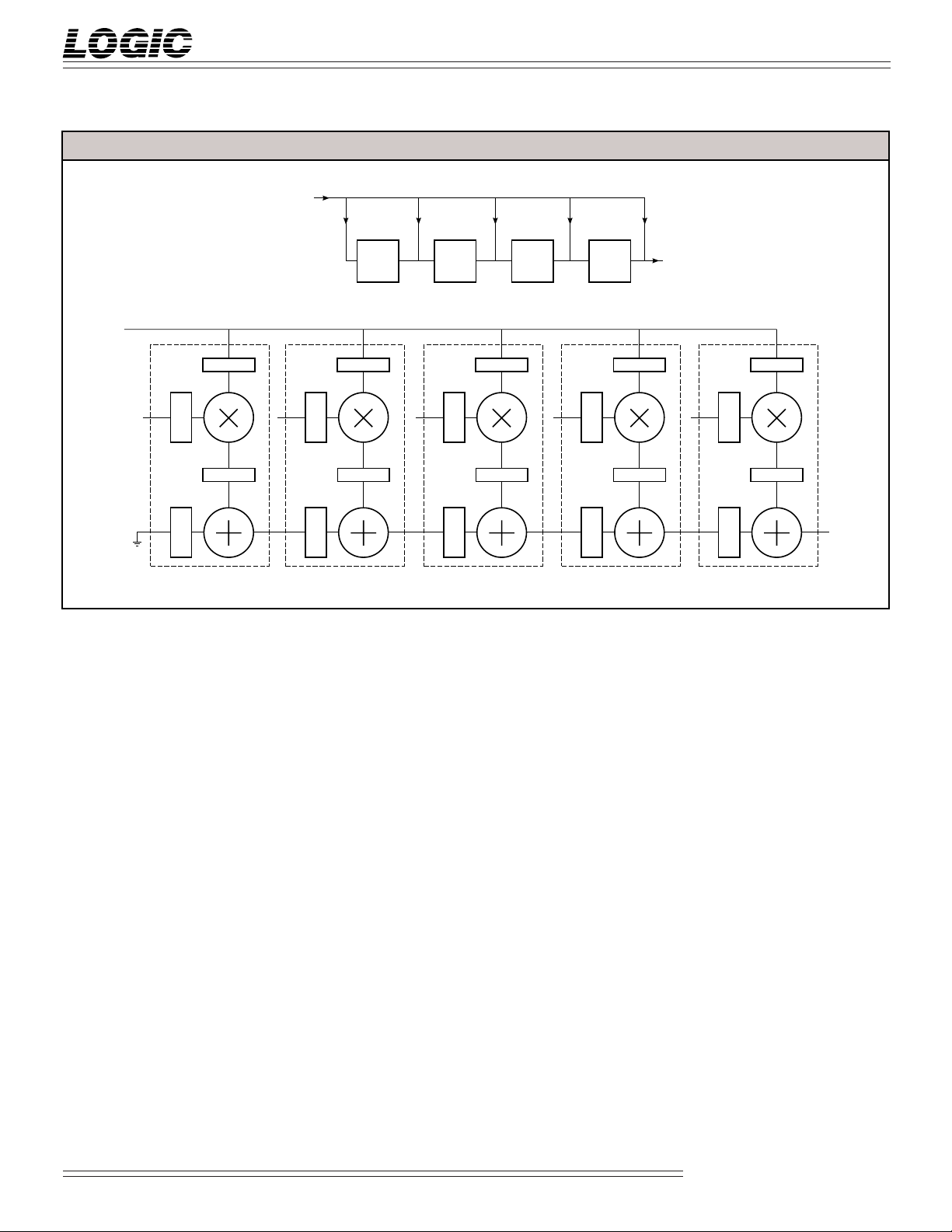
FIGURE 1. FLOW DIAGRAM FOR 5-TAP FIR FILTER
x(n)
h
h
4
3
LMS12
12-bit Cascadable Multiplier-Summer
h
2
h
1
h
0
x(n)
A
4
h
4
–1
Z
h
Z
APPLICATIONS
The LMS12 is designed specifically for
high-speed FIR filtering applications
requiring a throughput rate of one
output sample per clock period. By
cascading LMS12 units, the transpose
form of the FIR transfer function is
implemented directly, with each of the
LMS12 units supplying one of the
filter weights, and the cascaded
summers accumulating the results.
The signal flow graph for a 5-tap FIR
filter and the equivalent implementation using LMS12’s is shown in
Figure 1.
–1
Z
A
3
3
–1
–1
Z
h
2
–1
Z
–1
Z
A
2
The operation of the 5-tap FIR filter
implementation of Figure 1 is depicted
in Table 1. The filter weights h4 - h0
are assumed to be latched in the B
input registers of the LMS12 units.
The x(n) data is applied in parallel to
the A input registers of all devices.
For descriptive purposes in the table,
the A register contents and sum
output data of each device is labelled
–1
Z
h1
–1
Z
y(n)
A
1
h
Z
A
0
0
–1
according to the index of the weight
applied by that device; i.e., S0 is
produced by the rightmost device,
which has h0 as its filter weight and
A0 as its input register contents. Each
column represents one clock cycle,
with the data passing a particular
point in the system illustrated across
each row.
y(n)
Multiplier-Summers
2
08/16/2000–LDS.S12-J
LMS12
DEVICES INCORPORATED
TABLE 1. TIMING EXAMPLE FOR 5-TAP NONDECIMATING FIR FILTER
CLK Cycle 1 2 3 4 56789
X(n) Xn Xn+1 Xn+2 Xn+3 Xn+4 Xn+5 Xn+6 Xn+7 Xn+8
A4 Register Xn Xn+1 Xn+2 Xn+3 Xn+4 Xn+5 Xn+6 Xn+7
Sum 4 h4Xn h4Xn+1 h4Xn+2 h4Xn+3 h4Xn+4 h4Xn+5 h4Xn+6
A3 Register Xn Xn+1 Xn+2 Xn+3 Xn+4 Xn+5 Xn+6 Xn+7
Sum 3 h3Xn h3Xn+1 h3Xn+2 h3Xn+3 h3Xn+4 h3Xn+5 h3Xn+6
+h4Xn–1 +h4Xn +h4Xn+1 +h4Xn+2 +h4Xn+3 +h4Xn+4 +h4Xn+5
A2 Register Xn Xn+1 Xn+2 Xn+3 Xn+4 Xn+5 Xn+6 Xn+7
Sum 2 h2Xn h2Xn+1 h2Xn+2 h2Xn+3 h2Xn+4 h2Xn+5 h2Xn+6
+h3Xn–1 +h3Xn +h3Xn+1 +h3Xn+2 +h3Xn+3 +h3Xn+4 +h3Xn+5
+h4Xn–2 +h4Xn–1 +h4Xn +h4Xn+1 +h4Xn+2 +h4Xn+3 +h4Xn+4
A1 Register Xn Xn+1 Xn+2 Xn+3 Xn+4 Xn+5 Xn+6 Xn+7
Sum 1 h1Xn h1Xn+1 h1Xn+2 h1Xn+3 h1Xn+4 h1Xn+5 h1Xn+6
+h2Xn–1 +h2Xn +h2Xn+1 +h2Xn+2 +h2Xn+3 +h2Xn+4 +h2Xn+5
+h3Xn–2 +h3Xn–1 +h3Xn +h3Xn+1 +h3Xn+2 +h3Xn+3 +h3Xn+4
+h4Xn–3 +h4Xn–2 +h4Xn–1 +h4Xn +h4Xn+1 +h4Xn+2 +h4Xn+3
A0 Register Xn Xn+1 Xn+2 Xn+3 Xn+4 Xn+5 Xn+6 Xn+7
Sum 0 h0Xn h0Xn+1 h0Xn+2 h0Xn+3 h0Xn+4 h0Xn+5 h0Xn+6
+h1Xn–1 +h1Xn +h1Xn+1 +h1Xn+2 +h1Xn+3 +h1Xn+4 +h1Xn+5
+h2Xn–2 +h2Xn–1 +h2Xn +h2Xn+1 +h2Xn+2 +h2Xn+3 +h2Xn+4
+h3Xn–3 +h3Xn–2 +h3Xn–1 +h3Xn +h3Xn+1 +h3Xn+2 +h3Xn+3
+h4Xn–4 +h4Xn–3 +h4Xn–2 +h4Xn–1 +h4Xn +h4Xn+1 +h4Xn+2
12-bit Cascadable Multiplier-Summer
FIGURE 2A.INPUT FORMATS
11 10 9 2 1 0
0
2–12
–2
–2
(Sign)
11 10 9 2 1 0
11
–2
(Sign)
2102
9
FIGURE 2B.OUTPUT FORMATS
25 24
3
2
–2
2
(Sign)
25 24
25
24
–2
2
(Sign)
A
IN
Fractional Two’s Complement
–102–11
2–92
Integer Two’s Complement
22212
0
Fractional Two’s Complement
23 22 21 14 13 12
1202–1
2
Integer Two’s Complement
23 22 21 14 13 12
23222221
2
2–82–92
2142132
–10
B
IN
11 10 9 2 1 0
0
–2
(Sign)
2–12
–2
2–92
–102–11
11 10 9 2 1 0
11
–2
(Sign)
2102
9
22212
0
11 10 9 2 1 0
–112–122–13
2
–202–212–22
2
11 10 9 2 1 0
12
1121029
2
22212
0
Multiplier-Summers
3
08/16/2000–LDS.S12-J

DEVICES INCORPORATED
LMS12
12-bit Cascadable Multiplier-Summer
MAXIMUM RATINGS
Storage temperature ........................................................................................................... –65°C to +150°C
Operating ambient temperature........................................................................................... –55°C to +125°C
VCC supply voltage with respect to ground............................................................................ –0.5 V to +7.0V
Input signal with respect to ground ........................................................................................ –3.0V to +7.0 V
Signal applied to high impedance output ............................................................................... –3.0V to +7.0 V
Output current into low outputs............................................................................................................. 25 mA
Latchup current ............................................................................................................................... > 400 mA
OPERATING CONDITIONS
Active Operation, Commercial 0°C to +70°C 4.75 V ≤ VCC ≤ 5.25 V
Active Operation, Military –55°C to +125°C 4.50V ≤ VCC ≤ 5.50 V
ELECTRICAL CHARACTERISTICS
Above which useful life may be impaired (Notes 1, 2, 3, 8)
To meet specified electrical and switching characteristics
Mode Temperature Range (Ambient) Supply Voltage
Over Operating Conditions (Note 4)
Symbol Parameter Test Condition Min Typ Max Unit
VOH Output High Voltage VCC = Min., IOH = –2.0 mA 2.4 V
VOL Output Low Voltage VCC = Min., IOL = 4.0 mA 0.5 V
VIH Input High Voltage 2.0 VCC V
V IL Input Low Voltage (Note 3) 0.0 0.8 V
IIX Input Current Ground ≤ VIN ≤ VCC (Note 12) ±20 µA
IOZ Output Leakage Current Ground ≤ VOUT ≤ VCC (Note 12) ±20 µA
ICC1 VCC Current, Dynamic (Notes 5, 6) 15 25 mA
ICC2 VCC Current, Quiescent (Note 7) 1.0 mA
Multiplier-Summers
4
08/16/2000–LDS.S12-J
DEVICES INCORPORATED
3
3
3
3
3
3
3
3
3
3
3
3
3
3
3
3
3
3
3
3
3
3
3
3
3
3
3
3
3
3
3
3
3
3
3
3
3
3
3
3
3
3
3
4
4
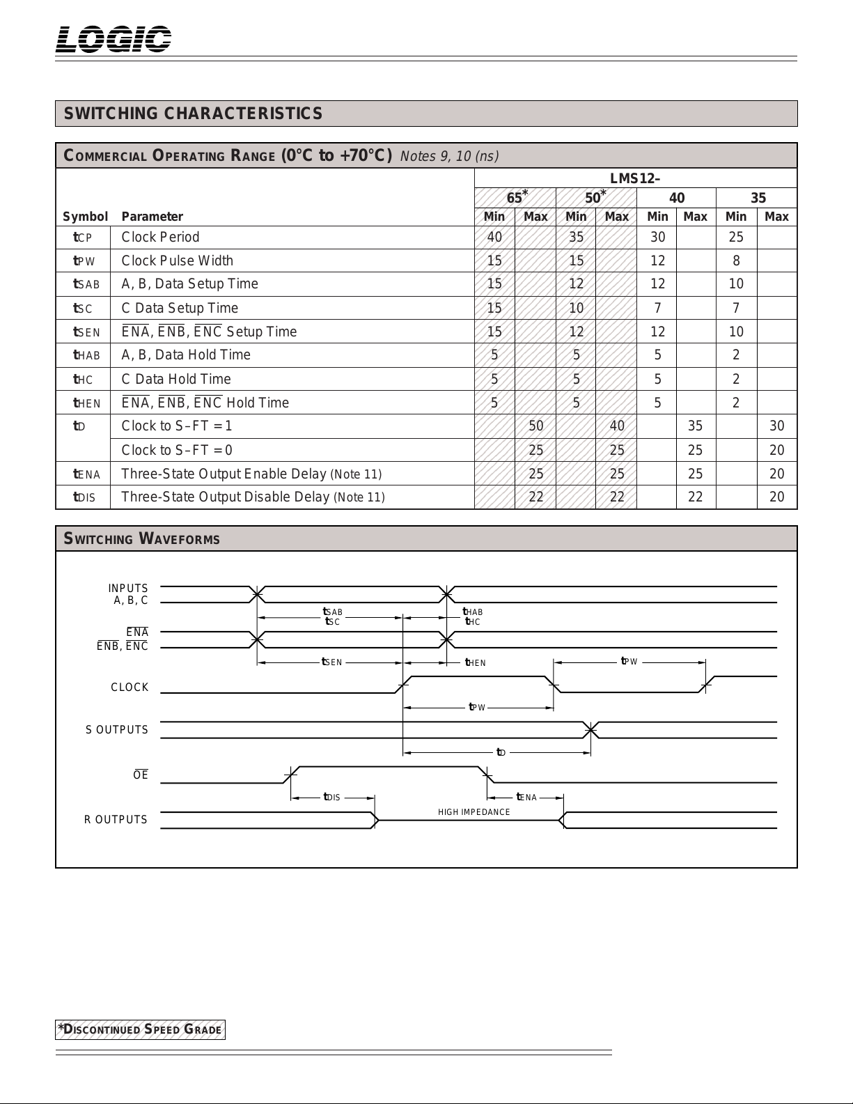
SWITCHING CHARACTERISTICS
LMS12
12-bit Cascadable Multiplier-Summer
COMMERCIAL OPERATING RANGE (0°C to +70°C)
Symbol Parameter Min Max Min Max Min Max Min Max
tCP Clock Period 40 35 30 25
tPW Clock Pulse Width 15 15 12 8
tSAB A, B, Data Setup Time 1 5 12 12 10
tSC C Data Setup Time 15 10 7 7
tSEN ENA, ENB, ENC Setup Time 15 12 12 10
tHAB A, B, Data Hold Time 5 5 5 2
tHC C Data Hold Time 5 5 5 2
tHEN ENA, ENB, ENC Hold Time 5 5 5 2
tD Clock to S–FT = 1 50 40 35 30
Clock to S–FT = 0 25 25 25 20
tENA Three-State Output Enable Delay (Note 11) 25 25 25 20
tDIS Three-State Output Disable Delay (Note 11) 22 22 22 20
Notes 9, 10 (ns)
234567890123456789012
234567890123456789012
234567890123456789012
234567890123456789012
234567890123456789012
234567890123456789012
234567890123456789012
234567890123456789012
234567890123456789012
234567890123456789012
234567890123456789012
234567890123456789012
234567890123456789012
234567890123456789012
234567890123456789012
234567890123456789012
234567890123456789012
234567890123456789012
234567890123456789012
234567890123456789012
234567890123456789012
234567890123456789012
234567890123456789012
234567890123456789012
234567890123456789012
234567890123456789012
234567890123456789012
234567890123456789012
234567890123456789012
234567890123456789012
234567890123456789012
234567890123456789012
234567890123456789012
234567890123456789012
234567890123456789012
234567890123456789012
234567890123456789012
234567890123456789012
234567890123456789012
234567890123456789012
234567890123456789012
234567890123456789012
234567890123456789012
65
LMS12–
*
50
*
40 35
SWITCHING WAVEFORMS
INPUTS
A, B, C
ENA
ENB, ENC
CLOCK
S OUTPUTS
OE
R OUTPUTS
2345678901234567890123
2345678901234567890123
*DISCONTINUED SPEED GRADE
t
t
SAB
t
SEN
t
DIS
SC
t
HAB
t
HC
t
HEN
t
HIGH IMPEDANCE
5
PW
t
PW
t
D
t
ENA
Multiplier-Summers
08/16/2000–LDS.S12-J

DEVICES INCORPORATED
2
2
2
2
2
2
2
2
2
2
2
2
2
2
2
2
2
2
2
2
2
2
2
2
2
2
2
2
2
2
2
2
2
2
2
2
2
2
2
2
2
2
2
4
4
SWITCHING CHARACTERISTICS
LMS12
12-bit Cascadable Multiplier-Summer
MILITARY OPERATING RANGE (–55°C to +125°C)
Symbol Parameter Min Max Min Max Min Max
tCP Clock Period 40 35 30
tPW Clock Pulse Width 15 15 12
tSAB A, B, Data Setup Time 15 15 12
tSC C Data Setup Time 15 15 12
tSEN ENA, ENB, ENC Setup Time 15 15 12
tHAB A, B, Data Hold Time 5 5 5
tHC C Data Hold Time 5 5 5
tHEN ENA, ENB, ENC Hold Time 5 5 5
tD Clock to S–FT = 1 50 45 35
Clock to S–FT = 0 25 25 25
tENA Three-State Output Enable Delay (Note 11) 25 25 25
tDIS Three-State Output Disable Delay (Note 11) 22 22 22
Notes 9, 10 (ns)
23456789012345678901234567890121
23456789012345678901234567890121
*
65
23456789012345678901234567890121
23456789012345678901234567890121
23456789012345678901234567890121
23456789012345678901234567890121
23456789012345678901234567890121
23456789012345678901234567890121
23456789012345678901234567890121
23456789012345678901234567890121
23456789012345678901234567890121
23456789012345678901234567890121
23456789012345678901234567890121
23456789012345678901234567890121
23456789012345678901234567890121
23456789012345678901234567890121
23456789012345678901234567890121
23456789012345678901234567890121
23456789012345678901234567890121
23456789012345678901234567890121
23456789012345678901234567890121
23456789012345678901234567890121
23456789012345678901234567890121
23456789012345678901234567890121
23456789012345678901234567890121
23456789012345678901234567890121
23456789012345678901234567890121
23456789012345678901234567890121
23456789012345678901234567890121
23456789012345678901234567890121
23456789012345678901234567890121
23456789012345678901234567890121
23456789012345678901234567890121
23456789012345678901234567890121
23456789012345678901234567890121
23456789012345678901234567890121
23456789012345678901234567890121
23456789012345678901234567890121
23456789012345678901234567890121
23456789012345678901234567890121
23456789012345678901234567890121
23456789012345678901234567890121
23456789012345678901234567890121
LMS12–
*
50
40
*
SWITCHING WAVEFORMS
INPUTS
A, B, C
ENA
ENB, ENC
CLOCK
S OUTPUTS
OE
R OUTPUTS
2345678901234567890123
2345678901234567890123
*DISCONTINUED SPEED GRADE
t
SAB
t
SC
t
SEN
t
DIS
t
HAB
t
HC
t
HEN
t
HIGH IMPEDANCE
6
PW
t
PW
t
D
t
ENA
Multiplier-Summers
08/16/2000–LDS.S12-J

DEVICES INCORPORATED
S1
I
OH
I
OL
V
TH
C
L
DUT
NOTES
LMS12
12-bit Cascadable Multiplier-Summer
1. Maximum Ratings indicate stress
specifications only. Functional operation of these products at values beyond
those indicated in the Operating Conditions table is not implied. Exposure to
maximum rating conditions for extended periods may affect reliability.
2. The products described by this specification include internal circuitry designed to protect the chip from damaging substrate injection currents and accumulations of static charge. Nevertheless, conventional precautions should
be observed during storage, handling,
and use of these circuits in order to
avoid exposure to excessive electrical
stress values.
3. This device provides hard clamping of
transient undershoot and overshoot. Input levels below ground or above VCC
will be clamped beginning at –0.6 V and
VCC + 0.6 V. The device can withstand
indefinite operation with inputs in the
range of –0.5 V to +7.0 V. Device operation will not be adversely affected, however, input current levels will be well in
excess of 100 mA.
4. Actual test conditions may vary from
those designated but operation is guaranteed as specified.
5. Supply current for a given application can be accurately approximated by:
2
NCV F
where
4
N = total number of device outputs
C = capacitive load per output
V = supply voltage
F = clock frequency
6. Tested with all outputs changing every cycle and no load, at a 5 MHz clock
rate.
7. Tested with all inputs within 0.1 V of
VCC or Ground, no load.
8. These parameters are guaranteed
but not 100% tested.
9. AC specifications are tested with
input transition times less than 3 ns,
output reference levels of 1.5 V (except
tDIS test), and input levels of nominally
0 to 3.0 V. Output loading may be a
resistive divider which provides for
specified IOH and IOL at an output
voltage of VOH min and VOL max
respectively. Alternatively, a diode
bridge with upper and lower current
sources of IOH and IOL respectively,
and a balancing voltage of 1.5 V may be
used. Parasitic capacitance is 30 pF
minimum, and may be distributed.
This device has high-speed outputs capable of large instantaneous current
pulses and fast turn-on/turn-off times.
As a result, care must be exercised in the
testing of this device. The following
measures are recommended:
a. A 0.1 µF ceramic capacitor should be
installed between VCC and Ground
leads as close to the Device Under Test
(DUT) as possible. Similar capacitors
should be installed between device VCC
and the tester common, and device
ground and tester common.
b. Ground and VCC supply planes
must be brought directly to the DUT
socket or contactor fingers.
c. Input voltages should be adjusted to
compensate for inductive ground and VCC
noise to maintain required DUT input
levels relative to the DUT ground pin.
10. Each parameter is shown as a minimum or maximum value. Input requirements are specified from the point
of view of the external system driving
the chip. Setup time, for example, is
specified as a minimum since the external system must supply at least that
much time to meet the worst-case requirements of all parts. Responses from
the internal circuitry are specified from
the point of view of the device. Output
delay, for example, is specified as a
maximum since worst-case operation of
any device always provides data within
that time.
11. For the tENA test, the transition is
measured to the 1.5 V crossing point
with datasheet loads. For the tDIS test,
the transition is measured to the
±200mV level from the measured
steady-state output voltage with
±10mA loads. The balancing voltage, VTH, is set at 3.5 V for Z-to-0
and 0-to-Z tests, and set at 0 V for Zto-1 and 1-to-Z tests.
12. These parameters are only tested at
the high temperature extreme, which is
the worst case for leakage current.
FIGURE A. OUTPUT LOADING CIRCUIT
FIGURE B. THRESHOLD LEVELS
t
VOL*
V
DIS
0.2 V
0.2 V
OH
*
3.5V Vth
0
1
0V Vth
t
ENA
OE
Z
Z
1.5 V 1.5 V
0
1
V
Measured V
OL
*
OH
*
V
Measured V
1.5 V
1.5 V
OL
with IOH = –10mA and IOL = 10mA
OH
with IOH = –10mA and IOL = 10mA
Z
Z
7
Multiplier-Summers
08/16/2000–LDS.S12-J

DEVICES INCORPORATED
ORDERING INFORMATION
84-pin
LMS12
12-bit Cascadable Multiplier-Summer
CLK
B
B
ENB
S
S
S
S
S
S
OE
FTS
V
B
B
B
B
B
B
B
B
CC
B1B0ENA
12
2
13
3
14
4
15
16
5
17
6
18
7
19
8
20
9
21
10
22
11
23
24
25
25
24
26
23
27
22
28
21
29
20
30
31
32
S19S18S17S16S15S14S13S12S11S
A11A10A9A8A7A6A5A4A3A2A1A0ENC
1234567
891011 78 77 76 75
84 83 82 81 80 79
C0C1C2C3C
Top
View
36353433 50 51 52 53
4443 45 46 47 493837 39 40 41 42
10
S9S8S7S6S5S4S3S2S1S
48
4
74
GND
73
C
5
72
C
6
71
C
7
70
C
8
69
C
9
68
C
10
67
C
11
66
C
12
65
C
13
64
C
14
63
C
15
62
C
16
61
C
17
60
C
18
59
C
19
58
C
20
57
C
21
56
C
22
55
C
23
54
C
24
0
25
C
Speed
40 ns
35 ns
Plastic J-Lead Chip Carrier
(J3)
0°C to +70°C — COMMERCIAL SCREENING
LMS12JC40
LMS12JC35
Multiplier-Summers
8
08/16/2000–LDS.S12-J
DEVICES INCORPORATED
1
1
1
1
1
1
1
1
1
1
1
1
1
1
1
1
1
1
1
1
1
1
1
1
1
1
1
1
1
1
1
1
1
1
1
1
1
1
1
1
1
1
1
1
1
1
1
1
1
1
1
1
1
1
1
1
1
1
1
1
1
1
1
1
1
1
1
12-bit Cascadable Multiplier-Summer
ORDERING INFORMATION
23456789012345678901234567890121234567890123456789012345678901212345678901234567890123456789012
23456789012345678901234567890121234567890123456789012345678901212345678901234567890123456789012
23456789012345678901234567890121234567890123456789012345678901212345678901234567890123456789012
84-pin
23456789012345678901234567890121234567890123456789012345678901212345678901234567890123456789012
23456789012345678901234567890121234567890123456789012345678901212345678901234567890123456789012
23456789012345678901234567890121234567890123456789012345678901212345678901234567890123456789012
23456789012345678901234567890121234567890123456789012345678901212345678901234567890123456789012
23456789012345678901234567890121234567890123456789012345678901212345678901234567890123456789012
23456789012345678901234567890121234567890123456789012345678901212345678901234567890123456789012
23456789012345678901234567890121234567890123456789012345678901212345678901234567890123456789012
23456789012345678901234567890121234567890123456789012345678901212345678901234567890123456789012
23456789012345678901234567890121234567890123456789012345678901212345678901234567890123456789012
23456789012345678901234567890121234567890123456789012345678901212345678901234567890123456789012
23456789012345678901234567890121234567890123456789012345678901212345678901234567890123456789012
23456789012345678901234567890121234567890123456789012345678901212345678901234567890123456789012
23456789012345678901234567890121234567890123456789012345678901212345678901234567890123456789012
23456789012345678901234567890121234567890123456789012345678901212345678901234567890123456789012
23456789012345678901234567890121234567890123456789012345678901212345678901234567890123456789012
23456789012345678901234567890121234567890123456789012345678901212345678901234567890123456789012
23456789012345678901234567890121234567890123456789012345678901212345678901234567890123456789012
23456789012345678901234567890121234567890123456789012345678901212345678901234567890123456789012
23456789012345678901234567890121234567890123456789012345678901212345678901234567890123456789012
23456789012345678901234567890121234567890123456789012345678901212345678901234567890123456789012
23456789012345678901234567890121234567890123456789012345678901212345678901234567890123456789012
23456789012345678901234567890121234567890123456789012345678901212345678901234567890123456789012
23456789012345678901234567890121234567890123456789012345678901212345678901234567890123456789012
23456789012345678901234567890121234567890123456789012345678901212345678901234567890123456789012
23456789012345678901234567890121234567890123456789012345678901212345678901234567890123456789012
23456789012345678901234567890121234567890123456789012345678901212345678901234567890123456789012
23456789012345678901234567890121234567890123456789012345678901212345678901234567890123456789012
23456789012345678901234567890121234567890123456789012345678901212345678901234567890123456789012
23456789012345678901234567890121234567890123456789012345678901212345678901234567890123456789012
23456789012345678901234567890121234567890123456789012345678901212345678901234567890123456789012
23456789012345678901234567890121234567890123456789012345678901212345678901234567890123456789012
23456789012345678901234567890121234567890123456789012345678901212345678901234567890123456789012
23456789012345678901234567890121234567890123456789012345678901212345678901234567890123456789012
23456789012345678901234567890121234567890123456789012345678901212345678901234567890123456789012
23456789012345678901234567890121234567890123456789012345678901212345678901234567890123456789012
23456789012345678901234567890121234567890123456789012345678901212345678901234567890123456789012
23456789012345678901234567890121234567890123456789012345678901212345678901234567890123456789012
23456789012345678901234567890121234567890123456789012345678901212345678901234567890123456789012
23456789012345678901234567890121234567890123456789012345678901212345678901234567890123456789012
23456789012345678901234567890121234567890123456789012345678901212345678901234567890123456789012
23456789012345678901234567890121234567890123456789012345678901212345678901234567890123456789012
23456789012345678901234567890121234567890123456789012345678901212345678901234567890123456789012
23456789012345678901234567890121234567890123456789012345678901212345678901234567890123456789012
23456789012345678901234567890121234567890123456789012345678901212345678901234567890123456789012
23456789012345678901234567890121234567890123456789012345678901212345678901234567890123456789012
23456789012345678901234567890121234567890123456789012345678901212345678901234567890123456789012
23456789012345678901234567890121234567890123456789012345678901212345678901234567890123456789012
23456789012345678901234567890121234567890123456789012345678901212345678901234567890123456789012
23456789012345678901234567890121234567890123456789012345678901212345678901234567890123456789012
23456789012345678901234567890121234567890123456789012345678901212345678901234567890123456789012
23456789012345678901234567890121234567890123456789012345678901212345678901234567890123456789012
23456789012345678901234567890121234567890123456789012345678901212345678901234567890123456789012
23456789012345678901234567890121234567890123456789012345678901212345678901234567890123456789012
23456789012345678901234567890121234567890123456789012345678901212345678901234567890123456789012
23456789012345678901234567890121234567890123456789012345678901212345678901234567890123456789012
23456789012345678901234567890121234567890123456789012345678901212345678901234567890123456789012
23456789012345678901234567890121234567890123456789012345678901212345678901234567890123456789012
23456789012345678901234567890121234567890123456789012345678901212345678901234567890123456789012
23456789012345678901234567890121234567890123456789012345678901212345678901234567890123456789012
23456789012345678901234567890121234567890123456789012345678901212345678901234567890123456789012
23456789012345678901234567890121234567890123456789012345678901212345678901234567890123456789012
23456789012345678901234567890121234567890123456789012345678901212345678901234567890123456789012
23456789012345678901234567890121234567890123456789012345678901212345678901234567890123456789012
23456789012345678901234567890121234567890123456789012345678901212345678901234567890123456789012
Speed
0°C to +70°C — COMMERCIAL SCREENING
–55°C to +125°C — COMMERCIAL SCREENING
–55°C to +125°C — MIL-STD-883 COMPLIANT
12345
A
A
ENA
B
1
B
2
B
4
B
B
C
B
3
CLK
D
B
5
6
B
E
B
B
8
B
9
F
B
7
ENB
B
G
S
S
24
25
S
H
S
21
S
22
J
FTS
S
20
K
S
19
OE
S
L
S
17
CC
V
S
6
A
A
A
A
6
7
5
8
A
3
A
4
Top View
A
9
11
A
10
0
10
Through Package
11
(i.e., Component Side Pinout)
23
S
10
S
9
S
15
S
12
S
18
S
14
16
13
S
11
S
8
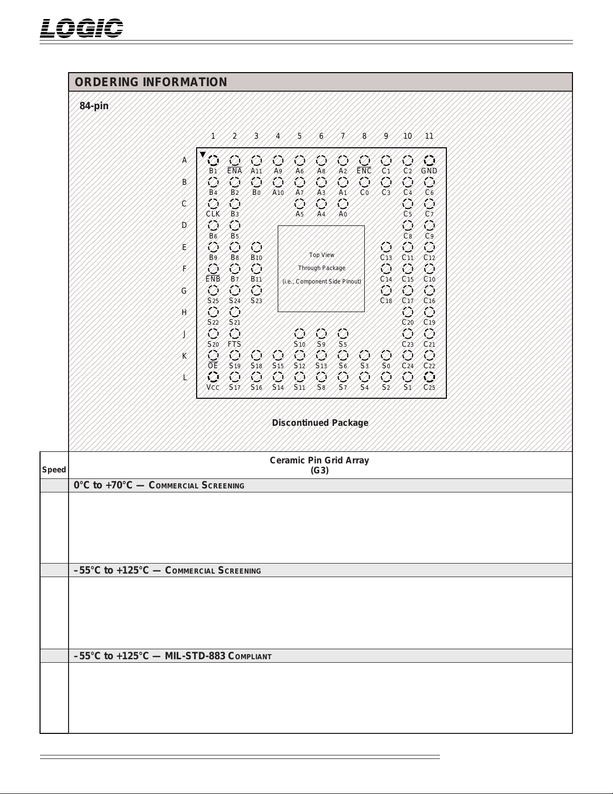
Discontinued Package
Ceramic Pin Grid Array
(G3)
9
7 8 9 10 11
A
2
ENC
C
1
C
2
GND
A
1
0
C
3
C
C
A
0
S
5
S
6
S
3
S
7
S
4
4
C
5
C
8
C
13
C
11
C
14
C
15
C
18
C
17
C
20
C
23
S
0
C
24
S
2
S
1
6
C
C
7
C
9
C
12
C
10
C
16
C
19
C
21
C
22
C
25
Multiplier-Summers
LMS12
08/16/2000–LDS.S12-J
 Loading...