

DEVICES INCORPORATED
LF9502
2K Programmable Line Buffer
LF9502
DEVICES INCORPORATED
FEATURES DESCRIPTION
❑❑
❑ 50 MHz Maximum Operating
❑❑
Frequency
❑❑
❑ Programmable Buffer Length from
❑❑
2 to 2049 Clock Cycles
❑❑
❑ 10-bit Data Inputs and Outputs
❑❑
❑❑
❑ Data Delay and Data Recirculation
❑❑
Modes
❑❑
❑ Supports Positive or Negative Edge
❑❑
System Clocks
❑❑
❑ Expandable Data Word Width or
❑❑
Buffer Length
❑❑
❑ 44-pin PLCC, J-Lead
❑❑
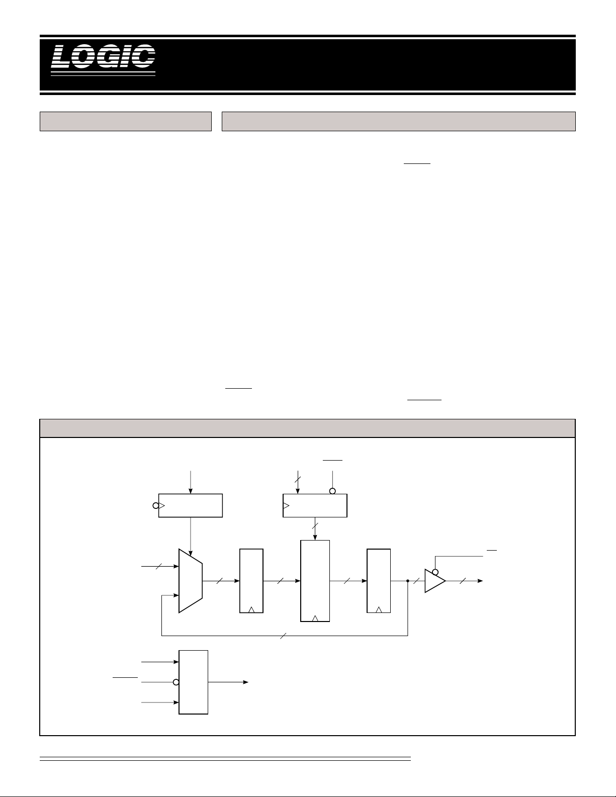
The LF9502 is a high-speed, 10-bit
programmable line buffer. Some
applications the LF9502 is useful for
include sample rate conversion, data
time compression/expansion, software controlled data alignment, and
programmable serial data shifting. By
using the MODSEL pin, two different
modes of operation can be selected:
delay mode and data recirculation
mode. The delay mode provides a
minimum of 2 to a maximum of 2049
clock cycles of delay between the
input and output of the device. The
data recirculation mode provides a
feedback path from the data output to
the data input for use as a programmable circular buffer.
By using the length control input
(LC10-0) and the length control enable
(LCEN) the length of the delay buffer
or amount of recirculation delay can
2K Programmable Line Buffer
be programmed. Providing a delay
value on the LC10-0 inputs and driving
LCEN LOW will load the delay value
into the length control register on the
next selected clock edge. Two registers, one preceeding the programmable delay RAM and one following,
are included in the delay path. Therefore, the programmed delay value
should equal the desired delay minus
2. This consequently means that the
value loaded into the length control
register must range from 0 to 2047 (to
provide an overall range of 2 to 2049).
The active edge of the clock input,
either positive or negative edge, can
be selected with the clock select
(CLKSEL) input. All timing is based
on the active clock edge selected by
CLKSEL. Data can be held temporarily by using the clock enable
(CLKEN) input.
LF9502 BLOCK DIAGRAM
DI9-0
CLKSEL
CLKEN
10
CLK
MODSEL
REGISTER
MUX
CLOCK
GENERATOR
10 10
REGISTER
TO ALL REGISTERS
LCO10-0 LCEN
11
REGISTER
11
PROGRAMMABLE
10
10
2K DELAY RAM
10
REGISTER
OE
10
DO
9-0
Video Imaging Products
1
08/16/2000–LDS.9502-G

DEVICES INCORPORATED
LF9502
2K Programmable Line Buffer
SIGNAL DEFINITIONS
Power
VCC and GND
+5 V power supply. All pins must be
connected.
Clock
CLK — Master Clock
The active edge of CLK, selected by
CLKSEL, strobes all registers. All
timing specifications are referenced to
the active edge of CLK.
Inputs
DI9-0 — Data Input
10-bit data, from the data input, is
latched into the device on the active
edge of CLK when MODSEL is LOW.
LC10-0 — Length Control Input
The 11-bit value is used to specify the
length of the delay buffer, between
DI9-0 and DO9-0, or the amount of
recirculation delay. An integer value
ranging from 0 to 2047 is used to
select a delay ranging from 2 to 2049
clock cycles. The value placed on the
LC10-0 inputs is equal to the desired
delay minus 2. The data presented on
LC10-0 is loaded into the device on the
active edge of CLK, selected by
CLKSEL, in conjunction with LCEN
being driven LOW.
Outputs
DO9-0 — Data Output
The 10-bit data output appears on
DO9-0 on the Nth clock cycle, where N
is the overall delay (desired delay).
Controls
LCEN — Length Control Enable
When LCEN is driven LOW, the next
active clock edge will cause the
loading of the delay value present at
the LC10-0 input.
OE — Output Enable
The Output Enable controls the state
of DO9-0. Driving OE LOW enables
the output port. When OE is HIGH,
DO9-0 is placed in a high-impedance
state. The internal transfer of data is
not affected by this control.
MODSEL — Mode Select
The Mode Select pin is used to choose
the desired mode of operation: data
delay mode or data recirculation
mode. Driving MODSEL LOW places
the device in the delay mode. The
device operates as a programmable
pipeline register. New data from the
DI9-0 input is loaded on every active
edge of CLK. Driving MODSEL
HIGH places the device in the data
recirculation mode. The device
operates as a programmable circular
buffer. The output of the device is
routed back to the input. MODSEL
may be changed during device
operation (synchronously), however,
the required setup and hold times,
with respect to CLK, must be met.
CLKSEL — Clock Select
The CLKSEL control allows the
selection of the active edge of CLK. A
LOW on CLKSEL selects negativeedge triggering of the device. Driving
CLKSEL HIGH selects positive-edge
triggering. All timing specifications
are referrenced to the selected active
edge of CLK.
CLKEN — Clock Enable
The Clock Enable control enables and
disables the CLK input. Driving
CLKEN LOW enables CLK and causes
the device to operate in a normal
fashion. When CLKEN is HIGH, CLK
is disabled and the device will hold all
internal operations and data. CLKEN
may be changed during device
operation (synchronously), however,
the required setup and hold times,
with respect to CLK, must be met.
The changing of CLKEN takes effect
on the active edge of CLK following
the edge in which it was latched.
Video Imaging Products
2
08/16/2000–LDS.9502-G
DEVICES INCORPORATED
LF9502
2K Programmable Line Buffer
MAXIMUM RATINGS
Storage temperature ........................................................................................................... –65°C to +150°C
Operating ambient temperature........................................................................................... –55°C to +125°C
VCC supply voltage with respect to ground............................................................................ –0.5 V to +7.0V
Input signal with respect to ground ............................................................................... –0.5 V to VCC + 0.5 V
Signal applied to high impedance output ...................................................................... –0.5 V to VCC + 0.5 V
Output current into low outputs............................................................................................................. 25 mA
Latchup current ............................................................................................................................... > 400 mA
OPERATING CONDITIONS
Active Operation, Commercial 0°C to +70°C 4.75 V ≤ VCC ≤ 5.25 V
ELECTRICAL CHARACTERISTICS
Symbol Parameter Test Condition Min Typ Max Unit
Above which useful life may be impaired (Notes 1, 2, 3, 8)
To meet specified electrical and switching characteristics
Mode Temperature Range (Ambient) Supply Voltage
Over Operating Conditions (Note 4)
VOH Output High Voltage VCC = Min., IOH = –4.0 mA 2.4 V
VOL Output Low Voltage VCC = Min., IOL = 4.0 mA 0.4 V
VIH Input High Voltage 2.0 VCC V
VIL Input Low Voltage (Note 3) 0.0 0.8 V
IIX Input Current Ground ≤ VIN ≤ VCC (Note 12) ±10 µA
IOZ Output Leakage Current Ground ≤ VOUT ≤ VCC (Note 12) ±10 µA
ICC1 VCC Current, Dynamic (Notes 5, 6) 125 mA
ICC2 VCC Current, Quiescent (Note 7) 500 µA
CIN Input Capacitance TA = 25°C, f = 1 MHz 10 pF
COUT Output Capacitance TA = 25°C, f = 1 MHz 10 pF
Video Imaging Products
3
08/16/2000–LDS.9502-G

DEVICES INCORPORATED
0
0
0
0
0
0
0
0
0
0
0
0
0
0
0
0
0
0
0
0
0
0
0
0
0
0
0
0
0
0
0
0
0
0
0
0
0
0
0
0
0
0
0
0
0
0
0
0
0
0
0
0
0
0
0
0
0
0
0
0
0
0
0
0
0
0
0
0
0
0
0
0
0
0
0
0
0
0
0
0
0
0
0
0
0
0
0
0
0
0
0
0
0
0
0
0
0
0
0
0
0
0
0
0
0
0
0
0
0
0
0
0
4
SWITCHING CHARACTERISTICS
LF9502
2K Programmable Line Buffer
COMMERCIAL OPERATING RANGE (0°C to +70°C)
Symbol Parameter Min Max Min Max Min Max Min Max Min Max
tCYC Cycle Time 40 31 25 20 15
tPW Clock Pulse Width 15 12 10 8 6
tDS Data Input Setup Time 12 10 8 6 5
tDH Data Input Hold Time 2 2 2 2 0
tES Clock Enable to Clock Setup Time 12 10 8 6 5
tEH Clock Enable to Clock Hold Time 2 2 2 2 0
tLS Length Control Input Setup Time 13 10 8 6 5
tLH Length Control Input Hold Time 2 2 2 2 0
tLES Length Control Enable to Clock Setup Time 12 10 8 6 5
tLEH Length Control Enable to Clock Hold Time 2 2 2 2 0
tMS Mode Select Setup Time 13 10 8 6 5
tMH Mode Select Hold Time 2 2 2 2 0
tOUT Clock to Data Out 22 16 15 14 10
tOH Output Hold Time (Note 8) 44444
tENA Three-State Output Enable Delay (Note 11) 25 24 15 14 12
tDIS Three-State Output Disable Delay (Note 11) 25 24 15 14 12
Notes 9, 10 (ns)
234567890123456789
234567890123456789
40
234567890123456789
234567890123456789
234567890123456789
234567890123456789
234567890123456789
234567890123456789
234567890123456789
234567890123456789
234567890123456789
234567890123456789
234567890123456789
234567890123456789
234567890123456789
234567890123456789
234567890123456789
234567890123456789
234567890123456789
234567890123456789
234567890123456789
234567890123456789
234567890123456789
234567890123456789
234567890123456789
234567890123456789
234567890123456789
234567890123456789
234567890123456789
234567890123456789
234567890123456789
234567890123456789
234567890123456789
234567890123456789
234567890123456789
234567890123456789
234567890123456789
234567890123456789
234567890123456789
234567890123456789
234567890123456789
234567890123456789
234567890123456789
234567890123456789
234567890123456789
234567890123456789
234567890123456789
234567890123456789
234567890123456789
234567890123456789
234567890123456789
234567890123456789
234567890123456789
234567890123456789
234567890123456789
234567890123456789
LF9502–
*
31
*
23456789
25 20 15
23456789
23456789
23456789
23456789
23456789
23456789
23456789
23456789
23456789
23456789
23456789
23456789
23456789
23456789
23456789
23456789
23456789
23456789
23456789
23456789
23456789
23456789
23456789
23456789
23456789
23456789
23456789
23456789
23456789
23456789
23456789
23456789
23456789
23456789
23456789
23456789
23456789
23456789
23456789
23456789
23456789
23456789
23456789
23456789
23456789
23456789
23456789
23456789
23456789
23456789
23456789
23456789
23456789
23456789
23456789
*
FUNCTIONAL TIMING — CLKSEL LOW
CYC
t
CLK*
*When CLKSEL is HIGH, assume CLK is inverted.
2345678901234567890123
*DISCONTINUED SPEED GRADE
MODSEL
DI
9-0
DO
9-0
OE
t
t
MS
PW
t
t
DS
OH
t
OUT
t
PW
t
MH
t
DH
HIGH IMPEDANCE
t
DIS
t
ENA
Video Imaging Products
4
08/16/2000–LDS.9502-G

DEVICES INCORPORATED
0
0
0
0
0
0
0
0
0
0
0
0
0
0
0
0
0
0
0
0
0
0
0
0
0
0
0
0
0
0
0
0
0
0
0
0
0
0
0
0
0
0
0
0
0
0
0
0
0
0
0
0
0
0
0
0
0
0
0
0
0
0
0
0
0
0
0
0
0
0
0
0
0
0
0
0
0
0
0
0
0
0
0
0
0
0
0
0
0
0
0
0
0
0
0
0
0
0
0
0
0
0
0
0
0
0
0
0
0
0
0
0
4
SWITCHING CHARACTERISTICS
LF9502
2K Programmable Line Buffer
COMMERCIAL OPERATING RANGE (0°C to +70°C)
Symbol Parameter Min Max Min Max Min Max Min Max Min Max
tCYC Cycle Time 40 31 25 20 15
tPW Clock Pulse Width 15 12 10 8 6
tDS Data Input Setup Time 12 10 8 6 5
tDH Data Input Hold Time 2 2 2 2 0
tES Clock Enable to Clock Setup Time 12 10 8 6 5
tEH Clock Enable to Clock Hold Time 2 2 2 2 0
tLS Length Control Input Setup Time 13 10 8 6 5
tLH Length Control Input Hold Time 2 2 2 2 0
tLES Length Control Enable to Clock Setup Time 13 10 8 6 5
tLEH Length Control Enable to Clock Hold Time 2 2 2 2 0
tMS Mode Select Setup Time 13 10 8 6 5
tMH Mode Select Hold Time 2 2 2 2 0
tOUT Clock to Data Out 22 16 15 14 10
tOH Output Hold Time (Note 8) 44444
tENA Three-State Output Enable Delay (Note 11) 25 20 15 14 12
tDIS Three-State Output Disable Delay (Note 11) 25 24 15 14 12
Notes 9, 10 (ns)
234567890123456789
234567890123456789
40
234567890123456789
234567890123456789
234567890123456789
234567890123456789
234567890123456789
234567890123456789
234567890123456789
234567890123456789
234567890123456789
234567890123456789
234567890123456789
234567890123456789
234567890123456789
234567890123456789
234567890123456789
234567890123456789
234567890123456789
234567890123456789
234567890123456789
234567890123456789
234567890123456789
234567890123456789
234567890123456789
234567890123456789
234567890123456789
234567890123456789
234567890123456789
234567890123456789
234567890123456789
234567890123456789
234567890123456789
234567890123456789
234567890123456789
234567890123456789
234567890123456789
234567890123456789
234567890123456789
234567890123456789
234567890123456789
234567890123456789
234567890123456789
234567890123456789
234567890123456789
234567890123456789
234567890123456789
234567890123456789
234567890123456789
234567890123456789
234567890123456789
234567890123456789
234567890123456789
234567890123456789
234567890123456789
234567890123456789
LF9502–
*
31
*
23456789
25 20 15
23456789
23456789
23456789
23456789
23456789
23456789
23456789
23456789
23456789
23456789
23456789
23456789
23456789
23456789
23456789
23456789
23456789
23456789
23456789
23456789
23456789
23456789
23456789
23456789
23456789
23456789
23456789
23456789
23456789
23456789
23456789
23456789
23456789
23456789
23456789
23456789
23456789
23456789
23456789
23456789
23456789
23456789
23456789
23456789
23456789
23456789
23456789
23456789
23456789
23456789
23456789
23456789
23456789
23456789
23456789
*
CLOCK ENABLE TIMING — CLKSEL LOW
CLK*
LENGTH CONTROL TIMING — CLKSEL LOW
*When CLKSEL is HIGH, assume CLK is inverted.
2345678901234567890123
*DISCONTINUED SPEED GRADE
CLKEN
INTERNAL
CLOCK
CLK*
LCEN
LC
10-0
t
LES
t
LS
t
ES
t
LEH
t
LH
t
PW
t
t
ES
MH
t
MH
Video Imaging Products
5
08/16/2000–LDS.9502-G

DEVICES INCORPORATED
NOTES
LF9502
2K Programmable Line Buffer
1. Maximum Ratings indicate stress
specifications only. Functional operation of these products at values beyond
those indicated in the Operating Conditions table is not implied. Exposure to
maximum rating conditions for extended periods may affect reliability.
2. The products described by this specification include internal circuitry designed to protect the chip from damaging substrate injection currents and accumulations of static charge. Nevertheless, conventional precautions should
be observed during storage, handling,
and use of these circuits in order to
avoid exposure to excessive electrical
stress values.
3. This device provides hard clamping of
transient undershoot and overshoot. Input levels below ground or above VCC
will be clamped beginning at –0.6 V and
VCC + 0.6 V. The device can withstand
indefinite operation with inputs in the
range of –0.5 V to +7.0 V. Device operation will not be adversely affected, however, input current levels will be well in
excess of 100 mA.
4. Actual test conditions may vary from
those designated but operation is guaranteed as specified.
5. Supply current for a given application can be accurately approximated by:
2
NCV F
where
4
N = total number of device outputs
C = capacitive load per output
V = supply voltage
F = clock frequency
6. Tested with all outputs changing every cycle and no load, at a 25 MHz clock
rate.
7. Tested with all inputs within 0.1 V of
VCC or Ground, no load.
8. These parameters are guaranteed
but not 100% tested.
9. AC specifications are tested with
input transition times less than 3 ns,
output reference levels of 1.5 V (except
tDIS test), and input levels of nominally
0 to 3.0 V. Output loading may be a
resistive divider which provides for
specified IOH and IOL at an output
voltage of VOH min and VOL max
respectively. Alternatively, a diode
bridge with upper and lower current
sources of IOH and IOL respectively,
and a balancing voltage of 1.5 V may be
used. Parasitic capacitance is 30 pF
minimum, and may be distributed.
This device has high-speed outputs capable of large instantaneous current
pulses and fast turn-on/turn-off times.
As a result, care must be exercised in the
testing of this device. The following
measures are recommended:
a. A 0.1 µF ceramic capacitor should be
installed between VCC and Ground
leads as close to the Device Under Test
(DUT) as possible. Similar capacitors
should be installed between device VCC
and the tester common, and device
ground and tester common.
b. Ground and VCC supply planes
must be brought directly to the DUT
socket or contactor fingers.
c. Input voltages should be adjusted to
compensate for inductive ground and VCC
noise to maintain required DUT input
levels relative to the DUT ground pin.
10. Each parameter is shown as a minimum or maximum value. Input requirements are specified from the point
of view of the external system driving
the chip. Setup time, for example, is
specified as a minimum since the external system must supply at least that
much time to meet the worst-case requirements of all parts. Responses from
the internal circuitry are specified from
the point of view of the device. Output
delay, for example, is specified as a
maximum since worst-case operation of
any device always provides data within
that time.
11. For the tENA test, the transition is
measured to the 1.5 V crossing point
with datasheet loads. For the tDIS test,
the transition is measured to the
±200mV level from the measured
steady-state output voltage with
±10mA loads. The balancing voltage, VTH, is set at 3.5 V for Z-to-0
and 0-to-Z tests, and set at 0 V for Zto-1 and 1-to-Z tests.
12. These parameters are only tested at
the high temperature extreme, which is
the worst case for leakage current.
FIGURE A. OUTPUT LOADING CIRCUIT
DUT
S1
I
OL
V
C
L
I
TH
OH
FIGURE B. THRESHOLD LEVELS
t
VOL*
V
DIS
0.2 V
0.2 V
OH
*
3.5V Vth
0
Z
Z
1
0V Vth
t
ENA
OE
1.5 V 1.5 V
Z
0
1
Z
V
OL
*
OH
*
V
Measured V
Measured V
1.5 V
1.5 V
OL
with IOH = –10mA and IOL = 10mA
OH
with IOH = –10mA and IOL = 10mA
Video Imaging Products
6
08/16/2000–LDS.9502-G

DEVICES INCORPORATED
ORDERING INFORMATION
44-pin
DO0
DO1
DO2
DO3
DO4
VCC
GND
DO
DO6
DO7
DO8
LF9502
2K Programmable Line Buffer
2
LC3
LC4
LC5
LCEN
CLKSELNCNC
CLKEN
CLK
LC
44123456
Top
View
LC9
LC10
43 42 41 40
2524 26 27 281918 20 21 22 23
LC8
7
8
9
10
11
12
13
14
5
15
16
17
0
OE
LC
DO9
LC1
MODSEL
DI0
39
DI1
38
DI2
37
DI3
36
35
DI4
34
VCC
33
GND
32
5
DI
31
DI6
30
DI7
29
DI8
DI9
NC
LC7
LC6
Speed
25 ns
20 ns
Plastic J-Lead Chip Carrier
(J1)
0°C to +70°C — COMMERCIAL SCREENING
LF9502JC25
LF9502JC20
–40°C to +85°C — COMMERCIAL SCREENING
Video Imaging Products
7
08/16/2000–LDS.9502-G
 Loading...