

Datasheet LF48908QC25, LF48908JC50, LF48908JC25, LF48908QC31, LF48908JC31 Datasheet (LOGIC)
DEVICES INCORPORATED
1
LF48908
Two Dimensional Convolver
1
2
3
4
5
6
7
8
9
10
11
08/9/2000–LDS.48908-J
Video Imaging Products
❑❑
❑❑
❑ 40 MHz Data and Computation
Rate
❑❑
❑❑
❑ Nine Multiplier Array with 8-bit
Data and 8-bit Coefficient Inputs
❑❑
❑❑
❑ Separate Cascade Input and Output
Ports
❑❑
❑❑
❑ On-board Programmable Row
Buffers
❑❑
❑❑
❑ Two Coefficient Mask Registers
❑❑
❑❑
❑ On-board 8-bit ALU
❑❑
❑❑
❑ Two’s Complement or Unsigned
Operands
❑❑
❑❑
❑ Replaces Harris HSP48908
❑❑
❑❑
❑ DECC SMD No. 5962-93007
❑❑
❑❑
❑ Package Styles Available:
• 84-pin Plastic LCC, J-Lead
• 100-pin Plastic Quad Flatpack
FEATURES DESCRIPTION
LF48908
Two Dimensional Convolver
DEVICES INCORPORATED
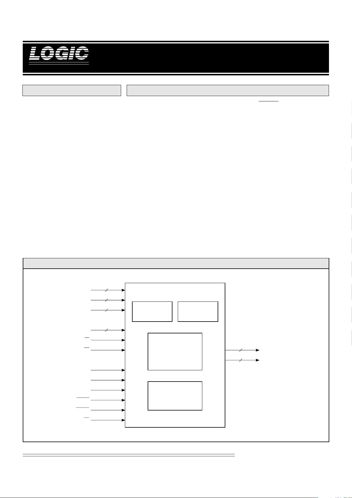
The LF48908 is a high-speed two
dimensional convolver that implements a 3 x 3 kernel convolution at
real-time video rates. Programmable
row buffers are located on-chip,
eliminating the need for external data
storage. Each row buffer can store up
to 1024 pixels. Two internal register
banks are provided allowing two
separate sets of filter coefficients to be
stored simultaneously. Adaptive filter
operations are possible when both
register banks are used. An on-chip
ALU is provided, allowing real-time
arithmetic and logical pixel point
operations to be performed on the
image data. The 3 x 3 convolver
comprises nine 8 x 8-bit multipliers,
various pipeline registers, and summers. A complete sum-of-products
operation is performed every clock
cycle. The FRAME signal resets all
data registers without affecting the
control and coefficient registers.
Pixel and coefficient input data are
both 8-bits and can be either signed or
unsigned integers. Image data should
be in a raster scan non-interlaced
format. The LF48908 can internally
store images as wide as 1024 pixels for
the 3 x 3 convolution. By using
external row buffers and multiple
LF48908s, longer pixel rows can be
used and convolutions with larger
kernel sizes can be performed. Output data is 20-bits and this guarantees
no overflow for kernel sizes up to 4 x 4.
A separate cascade input is used as
the data input for summing results
from multiple LF48908s. It can also
function as the data input path when
external line buffers are used.
FIGURE 1. LF48908 BLOCK DIAGRAM
DIN
7-0
CIN
9-0
CASO
7-0
A
2-0
LD
CS
CASI
15-0
CLK
HOLD
FRAME
RESET
OE
DOUT
19-0
16
3
8
8
20
8
EALU
3 x 3
CONVOLVER
ALU
ROW
BUFFERS
CONTROL
LOGIC
DEVICES INCORPORATED
LF48908
Two Dimensional Convolver
2
Video Imaging Products
08/9/2000–LDS.48908-J
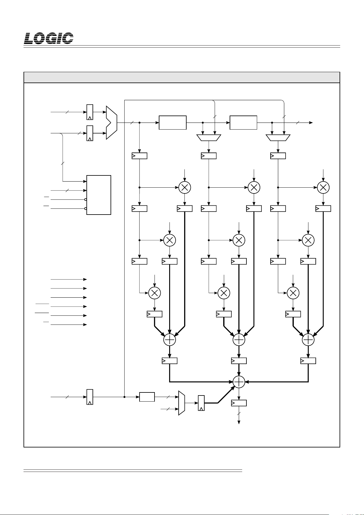
FIGURE 2. LF48908 FUNCTIONAL BLOCK DIAGRAM
DIN
7-0
1-4
CIN
9-0
2:1 2:1
ROW
BUFFER
ROW
BUFFER
CASO
7-0
7-0 15-8
A
2-0
LD
CS
CONTROL
LOGIC
CASI
15-0
2:1
SHIFT
0
CLK
HOLD
FRAME
RESET
OE
DOUT
19-0
I
H
G
F
E
D
C
B
A
ALU
REGISTER
ALU
20
20
16
3
8
8
10
20
8 8
8 8
7-0
EALU
NOTE: NUMBERS IN REGISTER INDICATE
NUMBER OF PIPELINE DELAYS.

DEVICES INCORPORATED
3
LF48908
Two Dimensional Convolver
1
2
3
4
5
6
7
8
9
10
11
08/9/2000–LDS.48908-J
Video Imaging Products
A2-0 — Control Logic Address Lines
A2-0 determines which Control Logic
Register will receive the CIN9-0 data.
CS — Chip Select
When CS is LOW, data can be loaded
into the Control Logic Registers.
When CS is HIGH, data can not be
loaded and the register contents will
not be changed.
LD — Load Strobe
If CS and LD are LOW, the data
present on CIN9-0 will be latched into
the Control Logic Register addressed
by A2-0 on the rising edge of LD.
FUNCTIONAL DESCRIPTION
The LF48908, a two-dimensional
convolver, executes convolutions using
internal row buffers to reduce design
complexity and board space requirements. 8-bit image data, in raster scan,
non-interlace format, is convolved with
one of two internal, 3 x 3 userprogramable filter kernels. Two 1024 x 8bit row buffers provide the data delay
needed to perform two-dimensional
convolutions on a single chip. The result
output of 20-bits allows for word growth
during the convolution operation.
The input data path (DIN7-0) provides
access to an 8-bit ALU. This allows
point operations to be performed on
the incoming data stream before
reaching the row buffers and the
convolver. The length of these buffers
is programmable for use in various
video formats without the need for
additional external delay.
This device is configured by loading
the coefficent data (filter kernels) and
row buffer length through the
coefficent data path (CIN7-0). Internal
registers are addressed using the A2-0
address lines. Chip Select (CS) and
Load Strobe (LD) complete the
configuration interface which may be
controlled by standard microprocessors without additional external logic.
SIGNAL DEFINITIONS
Power
VCC and GND
+5 V power supply. All pins must be
connected.
Clock
CLK — Master Clock
The rising edge of CLK strobes all
enabled registers except for the
Control Logic Registers.
Inputs
DIN7-0 — Pixel Data Input
DIN7-0 is the 8-bit registered pixel
data input port. Data is latched on the
rising edge of CLK.
CIN9-0 — Coefficient and Control Logic
Register Input
CIN7-0 is used to load the Coefficient
Registers or can be used to provide a
second operand input to the ALU.
CIN8-0 is used to load the Initialization Register. CIN9-0 is used to load
the ALU Microcode and Row Buffer
Length Registers. The Control Register Address Lines, A2-0, determine
which register will receive the CIN
data. The CIN data is loaded into the
addressed register by using the CS
and LD control inputs.
CASI15-0 — Cascade Input
The cascade input is used when
multiple LF48908s are cascaded
together or when external row buffers
are needed. This allows convolutions
of larger kernels or longer row sizes.
Outputs
DOUT19-0 — Data Output
DOUT19-0 is the 20-bit registered data
output port.
CASO7-0 — Cascade Output
The data presented on CASO7-0 is the
internal ALU output delayed by twice
the programmed internal row buffer
length.
Controls
RESET — Reset Control
When RESET is LOW, all internal
circuitry is reset, all outputs are forced
LOW, all Control Logic Registers are
loaded with their default values
(which is 0 for each one except the
ALU Microcode Register which has a
default value of “0000011000”), and all
other internal registers are loaded
with a “0”.
FRAME — New Frame Input Control
When asserted, FRAME signals the
start of a new frame. When FRAME is
LOW, all internal circuitry is reset
except for the ALU Microcode, Row
Length, Initialization, Coefficient, and
ALU Registers.
EALU — Enable ALU Register Input
When HIGH, data on CIN7-0 is latched
into the ALU Register on the next
rising edge of CLK. When LOW, data
on CIN7-0 will not be latched into the
ALU Register and the register contents will not be changed.
HOLD — Hold Control
The HOLD input is used to disable
CLK from all of the internal circuitry.
HOLD is latched on the rising edge of
CLK and takes effect on the next rising
edge of CLK. When HOLD is HIGH,
CLK will have no effect on the
LF48908 and all internal data will
remain unchanged.
OE — Output Enable
When OE is LOW, DOUT19-0 is
enabled for output. When OE is
HIGH, DOUT19-0 is placed in a highimpedance state.
DEVICES INCORPORATED
LF48908
Two Dimensional Convolver
4
Video Imaging Products
08/9/2000–LDS.48908-J
The filtered image data is output on
the Data Output bus (DOUT19-0). This
bus is registered with three-state
drivers to facilatate use on a standard
microprocessor system bus.
Data Input
Image data is input to the 3 x 3
convolver using DIN7-0. Data present
on DIN7-0 is latched into a programmable pipeline delay on the rising
edge of CLK. The programmable
pipeline delay (1 to 4 clock cycles)
allows for synchronization of input
data when multiple LF48908s are
cascaded together to perform larger
convolutions. This delay is programed via the Initialization Register
(see Table 3). The image data format,
unsigned or two’s complement, is also
controlled by this register.
Coefficient data is input to the 3 x 3
convolver using either of two Coefficient Registers (CREG0 or CREG1).
The Coefficient Registers are loaded
through CIN7-0 using the A2-0, CS, and
LD controls. The coefficient data
format, unsigned or two’s complement, is determined by the Initialization Register.
Arithmetic Logic Unit
The input data path ALU with shifter
allows pixel point operations to be
performed on the incoming image.
These operations include arithmetic
functions, logical masking, and left/
right shifts. The 10-bit ALU Microcode Register controls the various
operations. The three upper bits
control the shift amount and direction
while the seven lower bits determine
the arithmetic or logical operation.
The shift operation is performed on
the output of the ALU. This shift
operation is independent of the
arithmetic or logical operation of the
ALU.
Tables 1 and 2 show the operations of
the ALU Microcode Register. The “A”
operand comes from the DIN input
data path, while the “B” operand is
taken from the ALU Register. The
ALU Register is loaded using CIN7-0
and EALU. With EALU HIGH, data
from CIN7-0 is loaded into the ALU
Register on the rising edge of CLK.
With EALU LOW, the data is held in
the ALU Register. Since CIN7-0 is also
used to load the Control Logic Registers, it is possible to overwrite data in
those registers if CS and LD are active
when loading the ALU Register.
Therefore, special care must be taken
to ensure that CS and LD are not
active when writing to the ALU
Register.
Programmable Row Buffers
The two internal row buffers provide
the delay needed to perform the twodimensional convolution. The row
buffers function like 8-bit serial shift
registers with a user-programmable
delay from 1 to 1024 stages (it is
possible to select delay stages of 1 or
2, but this leads to meaningless results
for a 3 x 3 kernel convolution). The
row buffer length is set via the Row
Length Register (see Row Length
Register Section). The row buffers are
connected in series to provide the
proper pixel information to the
multiplier array. The Cascade Output
(CASO7-0) provides a 2X row delay of
the input data allowing for cascading
of LF48908s to handle larger frames
and/or kernel sizes. If more than 1024
delay stages are needed, it is possible
to use external row buffers and bypass
the internal row buffers. Bit 0 of the
Initialization Register determines if
internal or external row buffers are
used. If Bit 0 is a “0”, the internal row
buffers are used. If Bit 0 is a “1”, the
internal row buffers are bypassed and
external row buffers may be used.
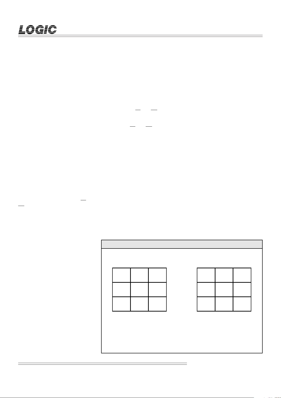
3 x 3 Multiplier Array
The multiplier array comprises nine
8 x 8-bit multipliers. The active
Coefficient Register supplies the
coefficents to each of the multipliers,
while the pixel data comes from the
data input path and row buffers. The
array forms a sum-of-products result
as defined by the equation listed in
Figure 3.
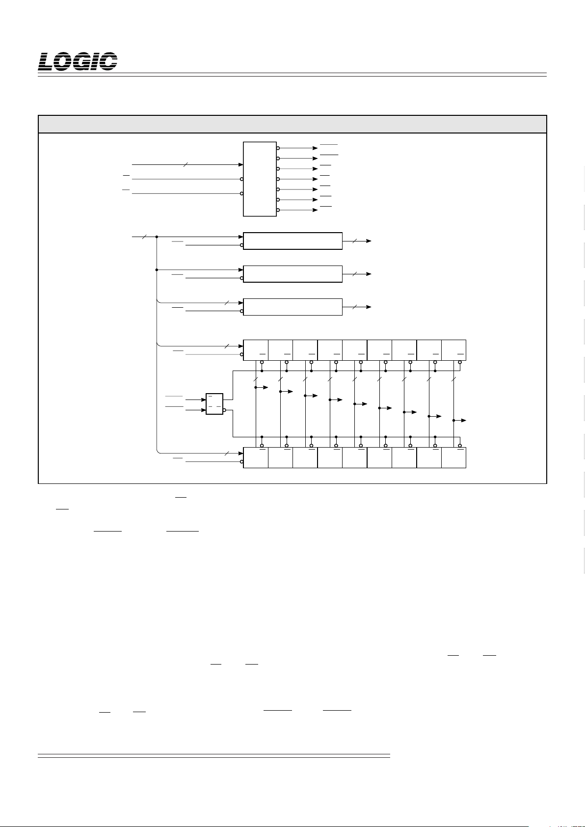
CONTROL LOGIC
Four sets of registers, the ALU Microcode, Row Length, Initialization, and
Coefficient, define the Control Logic
section. These registers are updated
FIGURE 3. MULTIPLIER ARRAY OUTPUT
P1 P2 P3
P4 P5 P6
P7 P8 P9
ABC
DEF
GH I
PIXEL INPUT DATA
FILTER KERNEL
MULTIPLIER ARRAY OUTPUT A(P1)=
+ D(P4)
+ G(P7)
+
+
+
B(P2)
E(P5)
H(P8)
+
+
+
C(P3)
F(P6)
I(P9)
DEVICES INCORPORATED
5
LF48908
Two Dimensional Convolver
1
2
3
4
5
6
7
8
9
10
11
08/9/2000–LDS.48908-J
Video Imaging Products
Row Length Register
The value stored in the Row Length
Register determines the number of
delay stages for each row buffer. The
number of delay stages should be set
equal to the row length of the input
image. The Row Length Register may
be loaded with the values 0 through
1023 (0 represents 1024 delay stages).
It is possible to program the row
buffers to have 1 or 2 delay stages, but
this will lead to meaningless results
for a 3 x 3 convolution. This register is
loaded through CIN9-0 using the A2-0,
CS, and LD controls. Once the Row
Length Register has been loaded, a
new value can not be loaded until the
LF48908 has been reset. This is done
by asserting RESET. After RESET goes
HIGH, the Row Length Register must
be loaded within 1024 CLK cycles. If
the Row Length Register is not loaded
within 1024 CLK cycles, the register
will automatically be loaded with a “0”.
Initialization Register
The Initialization Register configures
various functions of the device
including: input data delay, input
data format, coefficent data format,
output rounding, cascade mode, and
cascade input shift (see Table 3). This
register is loaded through CIN8-0
using the A2-0, CS, and LD controls.
Coefficient Registers - CREG0, CREG1
The Coefficient Registers are used to
store the filter coefficients for the
multiplier array. Each Coefficient
through the CIN bus using A2-0, CS,
and LD (see Figure 4). All the Control
Logic Registers are set to their default
values when RESET is active. FRAME
does not affect the values in these
registers.
ALU Microcode Register
Operation of the ALU and shifter are
determined by the value stored in the
ALU Microcode Register. This 10-bit
instruction word is divided into two
fields. The lower seven bits define the
arithmetic and logical operations of the
ALU. The upper three bits specify shift
distance and direction. Tables 1 and 2
detail the various instruction words.
This register is loaded through CIN9-0
using the A2-0, CS, and LD controls.
Also see Arithmetic Logic Unit section.
FIGURE 4. LF48908 CONTROL LOGIC BLOCK DIAGRAM
A2-0
LD
CS
ADDRESS
DECODE
3
ENCR1
ENCR0
CAS
CR1
CR0
LMC
EOR
CIN9-0
10
ALU MICROCODE REGISTER
LMC
ALU MICROCODE
10
ROW LENGTH REGISTER
EOR
ROW LENGTH
10
INITIALIZATION REGISTER
CAS
INITIALIZATION DATA
9
8-0
I
0 H0 G0 F0 E0 D0 C0 B0 A0
CR0
CR1
SRQ
Q
OE OE OE OE OE OE OE OE OE
I1 H1 G1 F1 E1 D1 C1 B1 A1
OE
OE OE OE OE OE OE OE OE
ENCR1
ENCR0
I
H
G
F
E
D
C
B
A
8 8 8 8 8 8 8 8 8
COEFFICIENT REGISTER 0
COEFFICIENT REGISTER 1
9
7-0
8
7-0
8

DEVICES INCORPORATED
LF48908
Two Dimensional Convolver
6
Video Imaging Products
08/9/2000–LDS.48908-J
loaded is determined by the data on
A2-0 during the load operation. If
CREG0 is to be loaded, “010” must be
placed on A2-0 during the load operation. If CREG1 is to be loaded, “011”
must be placed on A2-0. If desired, the
Coefficient Register that is not being
used to send data to the multiplier
array can be loaded with coefficient
data while the LF48908 is in active
operation.
Address Decoder
The Address Decoder is used to load
the Control Logic Registers and to
determine which Coefficient Register
sends data to the multiplier array. To
load a Control Logic Register, the
address of the register must be placed
on A2-0, the data to be written must be
placed on the CIN bus, and CS and
LD must be asserted. The data is
TABLE 2. ALU LOGICAL AND ARITHMETIC OPERATIONSTABLE 1. ALU SHIFT OPERATIONS
ALU MICROCODE REGISTER
REGISTER BIT
9 8 7 OPERATION
0 0 0 No Shift (Default)
0 0 1 Shift Right 1
0 1 0 Shift Right 2
0 1 1 Shift Right 3
1 0 0 Shift Left 1
1 0 1 Shift Left 2
1 1 0 Shift Left 3
1 1 1 Not Valid
Register can hold nine 8-bit values.
This allows two different 3 x 3 filter
kernels to be stored simultaneously on
the LF48908. The outputs of CREG0
and CREG1 are connected to the
coefficient inputs of the multiplier
array (A through I). The register used
to supply the coefficient data is
determined by the address written to
the Address Decoder. If a “101” is
written to the Address Decoder,
CREG0 will provide the coefficient
data. If a “110” is written to the
Address Decoder, CREG1 will be used.
It is possible to switch between the
two Coefficient Registers in real time.
This facilitates adaptive filtering
operations. It is important to remember to meet the tLCS timing specification when switching the Coefficient
Registers. When a Coefficient Register
is selected to supply data to the
multiplier array (one of the registers is
always selected), all of its outputs are
enabled simultaneously. When RESET
is asserted, CREG0 is the default
register selected to supply the coefficient data.
CREG0 and CREG1 are loaded
through CIN7-0 using the A2-0, CS, and
LD controls. The nine coefficient
values are presented on CIN7-0 one by
one, in order from A to I. As each
value is placed on CIN7-0, it is latched
into the selected Coefficient Register
using CS and LD. The register to be
latched into the addressed register
when LD goes HIGH. To select a
Coefficient Register (CREG0 or
CREG1) to send data to the multiplier
array, the appropriate address must be
placed on A2-0, and CS and LD must
be asserted. When LD goes HIGH, the
addressed register will begin supplying coefficient data to the multiplier
array. Table 4 lists all of the register
addresses.
The Control Logic Registers can be
modified during active operation of
the LF48908. If this is done, it is very
important to meet the tLCS timing
specification. This is to ensure that the
outputs of the Control Logic Registers
have enough time to change before the
next rising edge of CLK. If tLCS is not
met, unexpected results may occur on
DOUT19-0 for one clock cycle. There
are two situations in which tLCS may
ALU MICROCODE REGISTER
REGISTER BIT
6 5 4 3 2 1 0 OPERATION
0 0 0 0 0 0 0 Logical (00000000)
1 1 1 1 0 0 0 Logical (11111111)
0 0 1 1 0 0 0 Logical (A) (Default)
0 1 0 1 0 0 0 Logical (B)
1 1 0 0 0 0 0 Logical (A)
1 0 1 0 0 0 0 Logical (B)
0 1 1 0 0 0 1 Arithmetic (A + B)
1 0 0 1 0 1 0 Arithmetic (A – B)
1 0 0 1 1 0 0 Arithmetic (B – A)
0 0 0 1 0 0 0 Logical (A AND B)
0 0 1 0 0 0 0 Logical (A AND B)
0 1 0 0 0 0 0 Logical (A AND B)
0 1 1 1 0 0 0 Logical (A OR B)
1 0 1 1 0 0 0 Logical (A OR B)
1 1 0 1 0 0 0 Logical (A OR B)
1 1 1 0 0 0 0 Logical (A NAND B)
1 0 0 0 0 0 0 Logical (A NOR B)
0 1 1 0 0 0 0 Logical (A XOR B)
1 0 0 1 0 0 0 Logical (A XNOR B)

DEVICES INCORPORATED
7
LF48908
Two Dimensional Convolver
1
2
3
4
5
6
7
8
9
10
11
08/9/2000–LDS.48908-J
Video Imaging Products
be ignored. If the LF48908 is not in
active operation or if the innactive
Coefficient Register is being written to
during active operation.
Cascade Operation
The Cascade Input lines (CASI15-0)
and Cascade Output lines (CASO7-0)
are used to allow convolutions of
kernel sizes larger than 3 x 3. The
Cascade Input lines are also used to
allow convolutions on row lengths
longer than 1024 pixels. The Cascade
Mode Bit (Bit 0) of the Initialization
Register determines the function of
the Cascade Input lines. If the Cascade Mode Bit is a “0”, then the
Cascade Input lines are to be used to
cascade multiple LF48908s together to
perform convolutions of larger kernel
sizes. CASI15-0 will be left shifted (by
an amount determined by bits 7 and 8
of the Initialization Register) and then
added to DOUT19-0. Cascading is
accomplished by connecting CASO7-0
and DOUT19-0 of one LF48908 to
DIN7-0 and CASI15-0 respectively of
another LF48908. If the Cascade
Mode Bit is a “1”, then the Cascade
Input lines are to be used with external row buffers to allow for longer
row lengths. In this mode, the Cascade Input lines are split into two 8-bit
data busses (CASI15-8 and CASI7-0)
which are fed directly into the multiplier array.
TABLE 3. INITIALIZATION REGISTER
BIT FUNCTION
0 CASCADE MODE
0 Multiplier input from internal row buffers
1 Multiplier input from external buffers
2 1 INPUT DATA DELAY
0 0 No data delay registers used
0 1 One data delay register used
1 0 Two data delay registers used
1 1 Three data delay registers used
3 INPUT DATA FORMAT
0 Unsigned integer format
1 Two’s complement format
4 COEFFICIENT DATA FORMAT
0 Unsigned integer format
1 Two’s complement format
6 5 OUTPUT ROUNDING
0 0 No rounding
0 1 Round to 16 bits (i.e. DOUT19-4)
1 0 Round to 8 bits (i.e. DOUT19-12)
1 1 Not valid
8 7 CASI15-0 INPUT SHIFT
0 0 No shift
0 1 Shift CASI15-0 left two
1 0 Shift CASI15-0 left four
1 1 Shift CASI15-0 left eight
A2-0 FUNCTION
000 Load Row Buffer Length
Register
001 Load ALU Microcode Register
010 Load Coefficient Register 0
011 Load Coefficient Register 1
100 Load Initialization Register
101 Select Coefficient Register 0
for Internal Processing
110 Select Coefficient Register 1
for Internal Processing
111 No Operation
TABLE 4. CONTROL LOGIC
ADDRESS MAP

DEVICES INCORPORATED
LF48908
Two Dimensional Convolver
8
Video Imaging Products
08/9/2000–LDS.48908-J
Symbol Parameter Test Condition Min Typ Max Unit
VOH Output High Voltage VCC = Min., IOH = –400 µA 2.8 V
VOL Output Low Voltage VCC = Min., IOL = 2.0 mA 0.4 V
VIH Input High Voltage 2.0 VCC V
V IL Input Low Voltage (Note 3) 0.0 0.8 V
IIX Input Current Ground ≤ VIN ≤ VCC (Note 12) ±10 µA
IOZ Output Leakage Current Ground ≤ VOUT ≤ VCC (Note 12) ±10 µA
ICC1 VCC Current, Dynamic (Notes 5, 6) 110 mA
ICC2 VCC Current, Quiescent (Note 7) 500 µA
CIN Input Capacitance TA = 25°C, f = 1 MHz 10 pF
COUT Output Capacitance TA = 25°C, f = 1 MHz 12 pF
OPERATING CONDITIONS
To meet specified electrical and switching characteristics
ELECTRICAL CHARACTERISTICS
Over Operating Conditions (Note 4)
Mode Temperature Range (Ambient) Supply Voltage
Active Operation, Commercial 0°C to +70°C 4.75 V ≤ VCC ≤ 5.25 V
Active Operation, Military –55°C to +125°C 4.50 V ≤ VCC ≤ 5.50V
Storage temperature ........................................................................................................... –65°C to +150°C
Operating ambient temperature........................................................................................... –55°C to +125°C
VCC supply voltage with respect to ground............................................................................ –0.5 V to +7.0V
Input signal with respect to ground ............................................................................... –0.5 V to VCC + 0.5 V
Signal applied to high impedance output ...................................................................... –0.5 V to VCC + 0.5 V
Output current into low outputs............................................................................................................. 25 mA
Latchup current ............................................................................................................................... > 400 mA
MAXIMUM RATINGS
Above which useful life may be impaired (Notes 1, 2, 3, 8)

DEVICES INCORPORATED
9
LF48908
Two Dimensional Convolver
1
2
3
4
5
6
7
8
9
10
11
08/9/2000–LDS.48908-J
Video Imaging Products
LF48908–
50 31 25
Symbol Parameter Min Max Min Max Min Max
tCYC Cycle Time 50 31 25
tPWH Clock Pulse Width High 20 12 8
tPWL Clock Pulse Width Low 20 13 8
tDS Data Input Setup Time 14 13 8
tDH Data Input Hold Time 0 0 0
tCS CIN7-0 Setup Time 16 14 10
tCH CIN7-0 Hold Time 0 0 0
tES EALU Setup Time 14 12 10
tEH EALU Hold Time 0 0 0
tD Output Delay 22 16 15
tENA Three-State Output Enable Delay (Note 11) 22 16 15
tDIS Three-State Output Disable Delay (Note 11) 32 28 8
COMMERCIAL OPERATING RANGE (0°C to +70°C)
Notes 9, 10 (ns)
SWITCHING CHARACTERISTICS
SWITCHING WAVEFORMS:CONVOLVER DATA I/O
CLK
tCYC
tPWL tPWH
DIN7-0
CASI15-0
tDS tDH
DOUT19-0
CASO7-0
tD
CIN7-0
tCS tCH
EALU
tES tEH
(ALU REG DATA)
OE
tD
tDIS tENA
HIGH IMPEDANCE

DEVICES INCORPORATED
LF48908
Two Dimensional Convolver
10
Video Imaging Products
08/9/2000–LDS.48908-J
234567890123456789012345678901212345678901234
5
234567890123456789012345678901212345678901234
5
234567890123456789012345678901212345678901234
5
234567890123456789012345678901212345678901234
5
234567890123456789012345678901212345678901234
5
234567890123456789012345678901212345678901234
5
234567890123456789012345678901212345678901234
5
234567890123456789012345678901212345678901234
5
234567890123456789012345678901212345678901234
5
234567890123456789012345678901212345678901234
5
234567890123456789012345678901212345678901234
5
234567890123456789012345678901212345678901234
5
234567890123456789012345678901212345678901234
5
234567890123456789012345678901212345678901234
5
234567890123456789012345678901212345678901234
5
234567890123456789012345678901212345678901234
5
234567890123456789012345678901212345678901234
5
234567890123456789012345678901212345678901234
5
234567890123456789012345678901212345678901234
5
234567890123456789012345678901212345678901234
5
234567890123456789012345678901212345678901234
5
234567890123456789012345678901212345678901234
5
234567890123456789012345678901212345678901234
5
234567890123456789012345678901212345678901234
5
234567890123456789012345678901212345678901234
5
234567890123456789012345678901212345678901234
5
234567890123456789012345678901212345678901234
5
234567890123456789012345678901212345678901234
5
234567890123456789012345678901212345678901234
5
234567890123456789012345678901212345678901234
5
234567890123456789012345678901212345678901234
5
234567890123456789012345678901212345678901234
5
234567890123456789012345678901212345678901234
5
234567890123456789012345678901212345678901234
5
234567890123456789012345678901212345678901234
5
234567890123456789012345678901212345678901234
5
234567890123456789012345678901212345678901234
5
234567890123456789012345678901212345678901234
5
234567890123456789012345678901212345678901234
5
234567890123456789012345678901212345678901234
5
234567890123456789012345678901212345678901234
5
234567890123456789012345678901212345678901234
5
234567890123456789012345678901212345678901234
5
LF48908–
50
*
37
*
25
*
Symbol Parameter Min Max Min Max Min Max
tCYC Cycle Time 50 37 25
tPWH Clock Pulse Width High 20 15 8
tPWL Clock Pulse Width Low 20 15 8
tDS Data Input Setup Time 17 16 8
tDH Data Input Hold Time 0 0 0
tCS CIN7-0 Setup Time 20 17 10
tCH CIN7-0 Hold Time 0 0 0
tES EALU Setup Time 17 15 10
tEH EALU Hold Time 0 0 0
tD Output Delay 28 19 15
tENA Three-State Output Enable Delay (Note 11) 28 19 15
tDIS Three-State Output Disable Delay (Note 11) 40 35 8
MILITARY OPERATING RANGE (–55°C to +125°C)
Notes 9, 10 (ns)
SWITCHING WAVEFORMS:CONVOLVER DATA I/O
CLK
tCYC
tPWL tPWH
DIN7-0
CASI15-0
tDS tDH
DOUT19-0
CASO7-0
tD
CIN7-0
tCS tCH
EALU
tES tEH
(ALU REG DATA)
OE
tD
tDIS tENA
HIGH IMPEDANCE
2345678901234567890123
4
2345678901234567890123
4
*DISCONTINUED SPEED GRADE

DEVICES INCORPORATED
11
LF48908
Two Dimensional Convolver
1
2
3
4
5
6
7
8
9
10
11
08/9/2000–LDS.48908-J
Video Imaging Products
1234567890123456789012345678901212345678901234
1
23456789012345678901234567890121234567890123
4
1
23456789012345678901234567890121234567890123
4
1
23456789012345678901234567890121234567890123
4
1
23456789012345678901234567890121234567890123
4
1
23456789012345678901234567890121234567890123
4
1
23456789012345678901234567890121234567890123
4
1
23456789012345678901234567890121234567890123
4
1
23456789012345678901234567890121234567890123
4
1
23456789012345678901234567890121234567890123
4
1
23456789012345678901234567890121234567890123
4
1
23456789012345678901234567890121234567890123
4
1
23456789012345678901234567890121234567890123
4
1
23456789012345678901234567890121234567890123
4
1
23456789012345678901234567890121234567890123
4
1
23456789012345678901234567890121234567890123
4
1
23456789012345678901234567890121234567890123
4
1
23456789012345678901234567890121234567890123
4
1
23456789012345678901234567890121234567890123
4
1
23456789012345678901234567890121234567890123
4
1
23456789012345678901234567890121234567890123
4
1
23456789012345678901234567890121234567890123
4
1
23456789012345678901234567890121234567890123
4
1
23456789012345678901234567890121234567890123
4
1
23456789012345678901234567890121234567890123
4
1
23456789012345678901234567890121234567890123
4
1
23456789012345678901234567890121234567890123
4
1
23456789012345678901234567890121234567890123
4
1
23456789012345678901234567890121234567890123
4
1
23456789012345678901234567890121234567890123
4
1234567890123456789012345678901212345678901234
COMMERCIAL OPERATING RANGE (0°C to +70°C)
Notes 9, 10 (ns)
LF48908–
50
*
37
*
25
*
Symbol Parameter Min Max Min Max Min Max
tLPW LD Pulse Width 20 15 8
tLCS LD Setup Time (Applies only during active operation) 37 30 15
tCDS Configuration Data Setup Time 20 17 10
tCDH Configuration Data Hold Time 0 0 0
tAS Address Setup Time 15 15 10
tAH Address Hold Time 0 0 0
tCSS CS Setup Time 0 0 0
tCSH CS Hold Time 0 0 0
MILITARY OPERATING RANGE (–55°C to +125°C)
Notes 9, 10 (ns)
SWITCHING WAVEFORMS:CONFIGURATION DATA
LD
CS
A
2-0
CIN
9-0
t
CDS
t
CDH
t
CSS
t
LPW
t
CSH
t
AS
t
AH
CLK
t
LCS
*
*applies only when the LF48908 is in active operation.
LF48908–
50 31 25
Symbol Parameter Min Max Min Max Min Max
tLPW LD Pulse Width 20 12 8
tLCS LD Setup Time (Applies only during active operation) 30 25 15
tCDS Configuration Data Setup Time 16 14 10
tCDH Configuration Data Hold Time 0 0 0
tAS Address Setup Time 13 13 10
tAH Address Hold Time 0 0 0
tCSS CS Setup Time 0 0 0
tCSH CS Hold Time 0 0 0
2345678901234567890123
4
2345678901234567890123
4
*DISCONTINUED SPEED GRADE

DEVICES INCORPORATED
LF48908
Two Dimensional Convolver
12
Video Imaging Products
08/9/2000–LDS.48908-J
1234567890123456789012345678901212345678901234
1
23456789012345678901234567890121234567890123
4
1
23456789012345678901234567890121234567890123
4
1
23456789012345678901234567890121234567890123
4
1
23456789012345678901234567890121234567890123
4
1
23456789012345678901234567890121234567890123
4
1
23456789012345678901234567890121234567890123
4
1
23456789012345678901234567890121234567890123
4
1
23456789012345678901234567890121234567890123
4
1
23456789012345678901234567890121234567890123
4
1
23456789012345678901234567890121234567890123
4
1
23456789012345678901234567890121234567890123
4
1
23456789012345678901234567890121234567890123
4
1
23456789012345678901234567890121234567890123
4
1
23456789012345678901234567890121234567890123
4
1
23456789012345678901234567890121234567890123
4
1
23456789012345678901234567890121234567890123
4
1
23456789012345678901234567890121234567890123
4
1
23456789012345678901234567890121234567890123
4
1
23456789012345678901234567890121234567890123
4
1
23456789012345678901234567890121234567890123
4
1234567890123456789012345678901212345678901234
LF48908–
50
*
37
*
25
*
Symbol Parameter Min Max Min Max Min Max
tHS HOLD Setup Time 14 13 9
tHH HOLD Hold Time 2 2 0
tFPW FRAME Pulse Width 50 37 8
tFS FRAME Setup Time 30 25 20
tRPW RESET Pulse Width 50 37 8
LF48908–
50 31 25
Symbol Parameter Min Max Min Max Min Max
tHS HOLD Setup Time 12 11 9
tHH HOLD Hold Time 1 1 0
tFPW FRAME Pulse Width 50 31 8
tFS FRAME Setup Time 25 21 20
tRPW RESET Pulse Width 50 31 8
COMMERCIAL OPERATING RANGE (0°C to +70°C)
Notes 9, 10 (ns)
MILITARY OPERATING RANGE (–55°C to +125°C)
Notes 9, 10 (ns)
SWITCHING WAVEFORMS:CONTROL SIGNALS
CLK
HOLD
t
HS
t
HH
RESET
t
RPW
FRAME
t
HS
t
FPW
t
FS
2345678901234567890123
4
2345678901234567890123
4
*DISCONTINUED SPEED GRADE

DEVICES INCORPORATED
13
LF48908
Two Dimensional Convolver
1
2
3
4
5
6
7
8
9
10
11
08/9/2000–LDS.48908-J
Video Imaging Products
1. Maximum Ratings indicate stress
specifications only. Functional operation of these products at values beyond
those indicated in the Operating Conditions table is not implied. Exposure to
maximum rating conditions for extended periods may affect reliability.
2. The products described by this specification include internal circuitry designed to protect the chip from damaging substrate injection currents and accumulations of static charge. Nevertheless, conventional precautions should
be observed during storage, handling,
and use of these circuits in order to
avoid exposure to excessive electrical
stress values.
3. This device provides hard clamping of
transient undershoot and overshoot. Input levels below ground or above VCC
will be clamped beginning at –0.6 V and
VCC + 0.6 V. The device can withstand
indefinite operation with inputs in the
range of –0.5 V to +7.0 V. Device operation will not be adversely affected, however, input current levels will be well in
excess of 100 mA.
4. Actual test conditions may vary from
those designated but operation is guaranteed as specified.
5. Supply current for a given application can be accurately approximated by:
where
N = total number of device outputs
C = capacitive load per output
V = supply voltage
F = clock frequency
6. Tested with all outputs changing every cycle and no load, at a 20 MHz clock
rate.
7. Tested with all inputs within 0.1 V of
VCC or Ground, no load.
8. These parameters are guaranteed
but not 100% tested.
NCV F
4
2
NOTES
9. AC specifications are tested with
input transition times less than 3 ns,
output reference levels of 1.5 V (except
tDIS test), and input levels of nominally
0 to 3.0 V. Output loading may be a
resistive divider which provides for
specified IOH and IOL at an output
voltage of VOH min and VOL max
respectively. Alternatively, a diode
bridge with upper and lower current
sources of IOH and IOL respectively,
and a balancing voltage of 1.5 V may be
used. Parasitic capacitance is 30 pF
minimum, and may be distributed.
This device has high-speed outputs capable of large instantaneous current
pulses and fast turn-on/turn-off times.
As a result, care must be exercised in the
testing of this device. The following
measures are recommended:
a. A 0.1 µF ceramic capacitor should be
installed between VCC and Ground
leads as close to the Device Under Test
(DUT) as possible. Similar capacitors
should be installed between device VCC
and the tester common, and device
ground and tester common.
b. Ground and VCC supply planes
must be brought directly to the DUT
socket or contactor fingers.
c. Input voltages should be adjusted to
compensate for inductive ground and VCC
noise to maintain required DUT input
levels relative to the DUT ground pin.
10. Each parameter is shown as a minimum or maximum value. Input requirements are specified from the point
of view of the external system driving
the chip. Setup time, for example, is
specified as a minimum since the external system must supply at least that
much time to meet the worst-case requirements of all parts. Responses from
the internal circuitry are specified from
the point of view of the device. Output
delay, for example, is specified as a
maximum since worst-case operation of
any device always provides data within
that time.
11. For the tENA test, the transition is
measured to the 1.5 V crossing point
with datasheet loads. For the tDIS test,
the transition is measured to the
±200mV level from the measured
steady-state output voltage with
±10mA loads. The balancing voltage, VTH, is set at 3.5 V for Z-to-0
and 0-to-Z tests, and set at 0 V for Zto-1 and 1-to-Z tests.
12. These parameters are only tested at
the high temperature extreme, which is
the worst case for leakage current.
S1
I
OH
I
OL
V
TH
C
L
DUT
OE
0.2 V
t
DIS
t
ENA
0.2 V
1.5 V 1.5 V
3.5V Vth
1
Z
0
Z
Z
1
Z
0
1.5 V
1.5 V
0V Vth
VOL*
V
OH
*
V
OL
*
V
OH
*
Measured V
OL
with IOH = –10mA and IOL = 10mA
Measured V
OH
with IOH = –10mA and IOL = 10mA
FIGURE B. THRESHOLD LEVELS
FIGURE A. OUTPUT LOADING CIRCUIT

DEVICES INCORPORATED
LF48908
Two Dimensional Convolver
14
Video Imaging Products
08/9/2000–LDS.48908-J
Plastic J-Lead Chip Carrier
(J3)
LF48908JC50
LF48908JC31
LF48908JC25
ORDERING INFORMATION
0°C to +70°C — COMMERCIAL SCREENING
Speed
50 ns
31 ns
25 ns
84-pin
1234567
74
73
72
71
70
69
68
67
66
65
64
63
62
61
60
59
58
57
56
55
54
84 83 82 81 80 79
4443 45 46 47 493837 39 40 41 42
12
13
14
15
16
17
18
19
20
21
22
23
24
25
26
27
28
29
30
31
32
48
Top
View
891011 78 77 76 75
36353433 50 51 52 53
CIN3
CIN4
CIN5
CIN6
CIN7
CIN8
CIN9
GND
CLK
V
CC
HOLD
LD
CS
A
2
A1
A0
EALU
CASI
15
CASI14
CASI13
CASI12
CASO6
CASO7
DOUT0
DOUT1
DOUT2
GND
DOUT
3
DOUT4
DOUT5
DOUT6
DOUT7
VCC
DOUT8
GND
DOUT
9
DOUT10
DOUT11
DOUT12
DOUT13
DOUT14
GND
CASI11
CASI10
CASI9
CASI8
CASI7
CASI6
CASI5
CASI4
CASI3
VCC
CASI2
CASI1
CASI0
FRAME
RESET
GND
DOUT
19
DOUT18
DOUT17
DOUT16
DOUT15
CIN2
CIN1
CIN0
DIN7
DIN6
DIN5
DIN4
DIN3
DIN2
DIN1
DIN0
VCCOEGND
CASO0CASO1
CASO2
CASO3
CASO4
GND
CASO
5
–40°C to +85°C — COMMERCIAL SCREENING

DEVICES INCORPORATED
15
LF48908
Two Dimensional Convolver
1
2
3
4
5
6
7
8
9
10
11
08/9/2000–LDS.48908-J
Video Imaging Products
Plastic Quad Flatpack
(Q2)
LF48908QC31
LF48908QC25
ORDERING INFORMATION
0°C to +70°C — COMMERCIAL SCREENING
Speed
31 ns
25 ns
100-pin
CIN1
CIN2
NC
NC
CIN
3
CIN4
CIN5
CIN6
CIN7
CIN8
CIN9
GND
GND
CLK
V
CC
VCC
HOLD
LD
CS
A
2
A1
A0
EALU
CASI
15
CASI14
CASI13
CASI12
NC
NC
CASI
11
CIN0
DIN7
DIN6
DIN5
DIN6
DIN3
DIN2
DIN1
DIN0
VCC
VCCOEGND
GND
CASO0CASO1
CASO2
CASO3
CASO4
GND
GND
CASO
5
NC
CASO
6
CASO7
DOUT0
DOUT1
DOUT2
GND
GND
DOUT
3
DOUT4
DOUT5
DOUT6
DOUT7
VCC
VCC
DOUT
8
GND
GND
DOUT
9
DOUT10
DOUT11
DOUT12
DOUT13
DOUT14
GND
GND
DOUT
15
DOUT16
CASI10
CASI9
CASI8
CASI7
CASI6
CASI5
CASI4
CASI3
VCC
VCC
CASI2
CASI1
CASI0
FRAME
RESET
GND
GND
DOUT
19
DOUT18
DOUT17
80
79
78
77
76
75
74
73
72
71
70
69
68
67
66
65
64
63
62
61
60
59
58
57
56
55
54
53
52
51
Top
View
1
2
3
4
5
6
7
8
9
10
11
12
13
14
15
16
17
18
19
20
21
22
23
24
25
26
27
28
29
30
31323334353637383940414243444546474849
50
100
99989796959493929190898887868584838281
–40°C to +85°C — COMMERCIAL SCREENING

DEVICES INCORPORATED
LF48908
Two Dimensional Convolver
16
Video Imaging Products
08/9/2000–LDS.48908-J
23456789012345678901234567890121234567890123456789012345678901212345678901234567890123456789012
1
23456789012345678901234567890121234567890123456789012345678901212345678901234567890123456789012
1
23456789012345678901234567890121234567890123456789012345678901212345678901234567890123456789012
1
23456789012345678901234567890121234567890123456789012345678901212345678901234567890123456789012
1
23456789012345678901234567890121234567890123456789012345678901212345678901234567890123456789012
1
23456789012345678901234567890121234567890123456789012345678901212345678901234567890123456789012
1
23456789012345678901234567890121234567890123456789012345678901212345678901234567890123456789012
1
23456789012345678901234567890121234567890123456789012345678901212345678901234567890123456789012
1
23456789012345678901234567890121234567890123456789012345678901212345678901234567890123456789012
1
23456789012345678901234567890121234567890123456789012345678901212345678901234567890123456789012
1
23456789012345678901234567890121234567890123456789012345678901212345678901234567890123456789012
1
23456789012345678901234567890121234567890123456789012345678901212345678901234567890123456789012
1
23456789012345678901234567890121234567890123456789012345678901212345678901234567890123456789012
1
23456789012345678901234567890121234567890123456789012345678901212345678901234567890123456789012
1
23456789012345678901234567890121234567890123456789012345678901212345678901234567890123456789012
1
23456789012345678901234567890121234567890123456789012345678901212345678901234567890123456789012
1
23456789012345678901234567890121234567890123456789012345678901212345678901234567890123456789012
1
23456789012345678901234567890121234567890123456789012345678901212345678901234567890123456789012
1
23456789012345678901234567890121234567890123456789012345678901212345678901234567890123456789012
1
23456789012345678901234567890121234567890123456789012345678901212345678901234567890123456789012
1
23456789012345678901234567890121234567890123456789012345678901212345678901234567890123456789012
1
23456789012345678901234567890121234567890123456789012345678901212345678901234567890123456789012
1
23456789012345678901234567890121234567890123456789012345678901212345678901234567890123456789012
1
23456789012345678901234567890121234567890123456789012345678901212345678901234567890123456789012
1
23456789012345678901234567890121234567890123456789012345678901212345678901234567890123456789012
1
23456789012345678901234567890121234567890123456789012345678901212345678901234567890123456789012
1
23456789012345678901234567890121234567890123456789012345678901212345678901234567890123456789012
1
23456789012345678901234567890121234567890123456789012345678901212345678901234567890123456789012
1
23456789012345678901234567890121234567890123456789012345678901212345678901234567890123456789012
1
23456789012345678901234567890121234567890123456789012345678901212345678901234567890123456789012
1
23456789012345678901234567890121234567890123456789012345678901212345678901234567890123456789012
1
23456789012345678901234567890121234567890123456789012345678901212345678901234567890123456789012
1
23456789012345678901234567890121234567890123456789012345678901212345678901234567890123456789012
1
23456789012345678901234567890121234567890123456789012345678901212345678901234567890123456789012
1
23456789012345678901234567890121234567890123456789012345678901212345678901234567890123456789012
1
23456789012345678901234567890121234567890123456789012345678901212345678901234567890123456789012
1
23456789012345678901234567890121234567890123456789012345678901212345678901234567890123456789012
1
23456789012345678901234567890121234567890123456789012345678901212345678901234567890123456789012
1
23456789012345678901234567890121234567890123456789012345678901212345678901234567890123456789012
1
23456789012345678901234567890121234567890123456789012345678901212345678901234567890123456789012
1
23456789012345678901234567890121234567890123456789012345678901212345678901234567890123456789012
1
23456789012345678901234567890121234567890123456789012345678901212345678901234567890123456789012
1
23456789012345678901234567890121234567890123456789012345678901212345678901234567890123456789012
1
23456789012345678901234567890121234567890123456789012345678901212345678901234567890123456789012
1
23456789012345678901234567890121234567890123456789012345678901212345678901234567890123456789012
1
23456789012345678901234567890121234567890123456789012345678901212345678901234567890123456789012
1
23456789012345678901234567890121234567890123456789012345678901212345678901234567890123456789012
1
23456789012345678901234567890121234567890123456789012345678901212345678901234567890123456789012
1
23456789012345678901234567890121234567890123456789012345678901212345678901234567890123456789012
1
23456789012345678901234567890121234567890123456789012345678901212345678901234567890123456789012
1
23456789012345678901234567890121234567890123456789012345678901212345678901234567890123456789012
1
23456789012345678901234567890121234567890123456789012345678901212345678901234567890123456789012
1
23456789012345678901234567890121234567890123456789012345678901212345678901234567890123456789012
1
23456789012345678901234567890121234567890123456789012345678901212345678901234567890123456789012
1
23456789012345678901234567890121234567890123456789012345678901212345678901234567890123456789012
1
23456789012345678901234567890121234567890123456789012345678901212345678901234567890123456789012
1
23456789012345678901234567890121234567890123456789012345678901212345678901234567890123456789012
1
23456789012345678901234567890121234567890123456789012345678901212345678901234567890123456789012
1
23456789012345678901234567890121234567890123456789012345678901212345678901234567890123456789012
1
23456789012345678901234567890121234567890123456789012345678901212345678901234567890123456789012
1
23456789012345678901234567890121234567890123456789012345678901212345678901234567890123456789012
1
23456789012345678901234567890121234567890123456789012345678901212345678901234567890123456789012
1
23456789012345678901234567890121234567890123456789012345678901212345678901234567890123456789012
1
23456789012345678901234567890121234567890123456789012345678901212345678901234567890123456789012
1
23456789012345678901234567890121234567890123456789012345678901212345678901234567890123456789012
1
23456789012345678901234567890121234567890123456789012345678901212345678901234567890123456789012
1
23456789012345678901234567890121234567890123456789012345678901212345678901234567890123456789012
1
Ceramic Pin Grid Array
(G6)
ORDERING INFORMATION
0°C to +70°C — COMMERCIAL SCREENING
Speed
–55°C to +125°C — MIL-STD-883 COMPLIANT
–55°C to +125°C — COMMERCIAL SCREENING
84-pin
A
B
C
D
E
F
G
H
J
K
L
Top View
Through Package
(i.e., Component Side Pinout)
12345
6
7 8 9 10 11
CIN
0
CIN
3
CIN
4
CIN
7
GND
V
CC
A
2
EALU
CASI
13
CASI
11
CASI
9
DIN
7
CIN
1
CIN
9
HOLD
LD
CASI
10
CASI
8
DIN
5
DIN
6
CASI
7
CASI
6
DIN
2
DIN
3
DIN
4
CASI
5
CASI
4
CASI
3
DIN
1
CASO
0
DIN
0
CASI
2
V
CC
RESET
OE
GND
V
CC
CASI
1
FRAME
CASI
0
CASO
1
CASO
2
DOUT
19
GND
CIN
2
CIN
5
CIN
6
CIN
8
CLK
A
1
CS
A
0
CASI
15
CASI
14
CASI
12
CASO
3
GND
DOUT
3
DOUT
7
V
CC
DOUT
16
DOUT
18
CASO
4
CASO
5
CASO
7
DOUT
2
DOUT
4
DOUT
9
GND
DOUT
11
DOUT
14
GND
DOUT
17
CASO
6
DOUT
0
DOUT
1
GND
DOUT
5
DOUT
6
DOUT
8
DOUT
10
DOUT
12
DOUT
13
DOUT
15
Discontinued Package
 Loading...