

DEVICES INCORPORATED
Video Imaging Products
1
LF48212
12 x 12-bit Alpha Mixer
08/16/2000–LDS.48212-F
❑❑
❑❑
❑ 50 MHz Data and Computation
Rate
❑❑
❑❑
❑ Two’s Complement or Unsigned
Operands
❑❑
❑❑
❑ On-board Programmable Delay
Stages
❑❑
❑❑
❑ Programmable Output Rounding
❑❑
❑❑
❑ Replaces Harris HSP48212
❑❑
❑❑
❑ Package Styles Available:
• 68-pin PLCC, J-Lead
• 64-pin PQFP
FEATURES DESCRIPTION
LF48212
12 x 12-bit Alpha Mixer
DEVICES INCORPORATED
The LF48212 is a high-speed video
alpha mixer capable of mixing video
signals at real-time video rates. It
takes two 12-bit video signals and
mixes them together using an alpha
mix factor . Alpha determines the
weighting that each video signal
receives during the mix operation.
The input video data can be in either
unsigned or two’s complement
format, but both inputs must be in the
same format. Independently controlled programmable delay stages are
provided for the input and control
signals to allow for allignment of
input data if necessary. The delay
stages can be programmed to have
from 0 to 7 delays. The 13-bit output
of the alpha mixer is registered with
three-state drivers and may be
rounded to 8, 10, 12, or 13-bits.
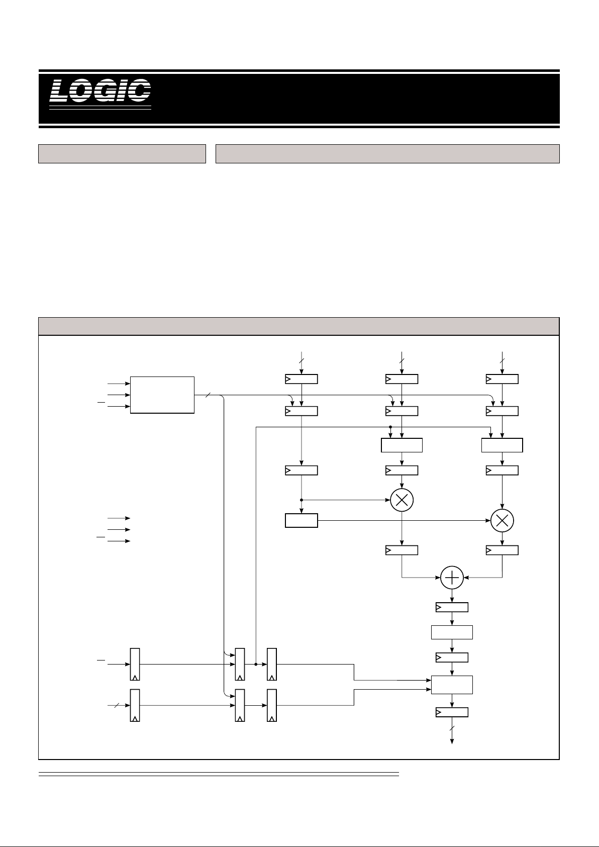
LF48212 BLOCK DIAGRAM
DINA
11-0
α
11-0
DINB
11-0
FORMAT
FORMAT
0-7
α
1.0 –
α
0-7
0-7
ADJUST
FORMAT
DOUT
12-0
0-70-7
TC
RND
1-0
DELAY CONTROL
REGISTER
BYPASS
DEL
LD
CLK
MIXEN
OE
NOTE: NUMBERS IN REGISTERS INDICATE
NUMBER OF PIPELINE DELAYS.
12 12 12
13
2
15
44
DEVICES INCORPORATED
LF48212
12 x 12-bit Alpha Mixer
2
Video Imaging Products
08/16/2000–LDS.48212-F
SIGNAL DEFINITIONS
Power
VCC and GND
+5 V power supply. All pins must be
connected.
Clock
CLK — Master Clock
The rising edge of CLK strobes all
enabled registers except for the Delay
Control Register .
Inputs
DINA11-0 — Pixel Data Input A
DINA11-0 is one of the 12-bit registered data input ports. Data is latched
on the rising edge of CLK.
DINB11-0 — Pixel Data Input B
DINB11-0 is the other 12-bit registered
data input port. Data is latched on the
rising edge of CLK.
α
11-0 — Alpha Mix Input
α11-0 determines the weighting
applied to the data input signals
before being mixed together. DINA11-0
and DINB11-0 receive weightings of α
and 1.0 – α respectively. α11-0 is
unsigned and restricted to the range of
0 to 1.0. Figure 1 shows the data
format for α11-0. If a value greater
than 1.0 is latched into the Alpha Mix
Input, internal circuitry will force the
value to be equal to 1.0. Data is
latched on the rising edge of CLK.
DEL — Delay Data Input
DEL is used to load the Delay Control
Register . The Delay Contr ol Register
contains a 15-bit value which determines the number of delay stages
added to the input and control signals.
The 15-bit data value is loaded serially
into the Delay Control Register using
DEL and LD. Data present on DEL is
latched on the rising edge of LD.
FIGURE 1. ALPHA MIX INPUT FORMAT
11 10 9 6 5 487 3210
2
02–12–2
2–52–62
–7
2–32
–4
2–82–92
–102–11
Outputs
DOUT12-0 — Data Output
DOUT12-0 is the 13-bit registered data
output port.
Controls
TC — Data Format Control
TC determines if the input data is in
unsigned or two’s complement
format. If TC is LOW, the data is in
two’s complement format. If TC is
HIGH, the data is in unsigned format.
Data present on TC is latched on the
rising edge of CLK. TC only affects
the data that is being latched into the
LF48212. Changing TC does not affect
internal data already in the pipeline.
MIXEN — Alpha Mix Input Enable
When HIGH, data on α11-0 is latched
into the LF48212 on the rising edge of
CLK. When LOW, data on α11-0 is not
latched and the last value loaded is
held as the alpha mix value.
LD — Load Strobe
The rising edge of LD latches the data
on DEL into the Delay Control Register.
BYPASS — Bypass Delay Stage Control
The BYPASS control is used to bypass
the internal programmable delay
stages. When BYPASS is set HIGH,
the Delay Control Register will
automatically be loaded with a “0”.
This will set the number of programmable delay stages to zero for all
input and control signals. When
BYPASS is LOW, the desired number
of delay stages can be set by loading
RND1-0 ROUNDING FORMAT
00 Round to 8-bits
01 Round to 10-bits
10 Round to 12-bits
11 Round to 13-bits
TABLE 1. OUTPUT ROUNDING
the Delay Control Register with the
appropriate value. Note that this
signal is not intended to change
during active operation of the
LF48212.
RND1-0 — Output Rounding Control
RND1-0 determines how the output of
the LF48212 is rounded. The output
may be rounded to 8, 10, 12, or 13-bits.
Table 1 lists the different rounding
possibilities and the associated value
for RND1-0. Rounding is accomplished by adding a “1” to the bit to
the right of what will become the least
significant bit. Then the bit that had
the “1” added to it and all bits to the
right of it are set to “0”. Data present
on RND1-0 is latched on the rising
edge of CLK. When RND1-0 is latched
in, it only applies to the video input
data latched in at the same time.
Changing RND1-0 does not affect the
rounding format for internal data
already in the pipeline.
OE — Output Enable
When OE is LOW, DOUT12-0 is
enabled for output. When OE is
HIGH, DOUT12-0 is placed in a highimpedance state.
DEVICES INCORPORATED
Video Imaging Products
3
LF48212
12 x 12-bit Alpha Mixer
08/16/2000–LDS.48212-F
FUNCTIONAL DESCRIPTION
The two video signals to be mixed
together are input to the LF48212
using DINA11-0 and DINB11-0. Data
present on DINA11-0 and DINB11-0 is
latched on the rising edge of CLK.
The input data may be in either
unsigned or two’s complement
format, but both inputs must be in the
same format. TC determines the
format of the input data. When TC is
HIGH, the input data is in unsigned
format. When TC is LOW, the input
data is in two’s complement format.
TC is latched on the rising edge of
CLK and only affects the input data
latched in at the same time. The data
already in the pipeline is not affected
when TC changes.
DINA11-0 and DINB11-0 are mixed
together using an alpha mix factor
(α11-0) as defined by the equation
listed in Figure 2. α11-0 is unsigned
and restricted to the range of 0 to 1.0.
MIXEN controls the loading of alpha
mix data. When MIXEN is HIGH,
data present on α11-0 is latched on the
rising edge of CLK. When MIXEN is
LOW, data present on α11-0 is not
latched and the last value loaded is
held as the alpha mix value.
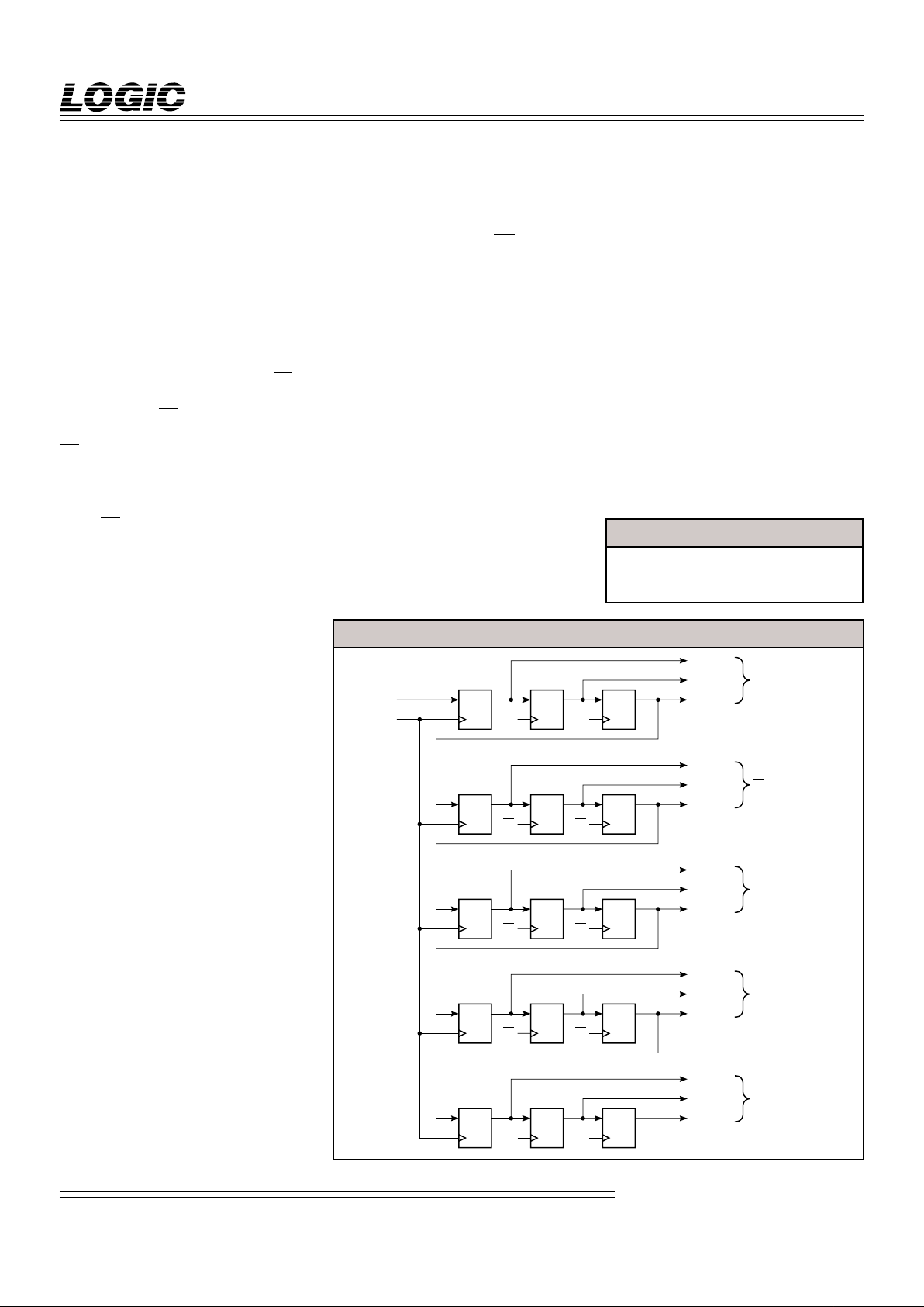
It is possible to add extra delay stages
to the input data and control signals
by using the programmable delay
stages. The 15-bit value (DELAY14-0)
stored in the Delay Control Register
determines the number of delay stages
added. DELAY14-0 is divided into 5
groups of 3-bits each. Each 3-bit
group contains the delay information
for one of the input data or control
signals. Figure 3 shows the block
diagram of the Delay Control Register
as well as a list of the input data and
control signals that may be delayed
and the DELAY signals that control
them. The delay length can be programmed to be from 0 to 7 stages. The
delay length is set by loading the
binary equivalent of the desired delay
length into the appropriate 3-bit
group. For example, to add four extra
delay stages to DINB11-0, DELAY5-3
should be set to “100”. DELAY14-0 is
loaded serially into the Delay Control
Register using DEL and LD. DELAY0
is the first value loaded and DELAY14
is the last. Data present on DEL is
latched on the rising edge of LD.
BYPASS is used to disable the programmable delay stages. When
BYPASS is HIGH, the Delay Control
Register is automatically loaded with
a “0”. This sets all programmable
delay stages to a length of zero. When
BYPASS is LOW, the Delay Control
Register may be loaded to set the
desired number of delay stages. Note
that BYPASS is not intended to change
during active operation of the
LF48212.
The Adjust stage of the LF48212 is
used to maximize the precision of the
output data. Since α can never be
larger than 1.0, the most significant bit
of the internal summer output is not
needed. The Adjust stage takes the
output of the internal summer and left
shifts the data one bit position. This
removes the MSB of the internal
summer output and provides one
more bit of precision for the output
data.
The output data of the LF48212 may
be rounded to 8, 10, 12, or 13-bits.
RND1-0 determines how the output is
rounded (See Table 1). RND1-0 is
latched on the rising edge of CLK and
only affects the input data latched in
at the same time. The data already in
the pipeline is not affected when
RND1-0 changes.
FIGURE 3. DELAY CONTROL REGISTER BLOCK DIAGRAM
DEL
LD
DQ DQ DQ
DELAY
14
DELAY
13
DELAY
12
LD LD
DQ DQ DQ
DELAY
11
DELAY
10
DELAY
9
LD LD
DQ DQ DQ
DELAY
8
DELAY
7
DELAY
6
LD LD
DQ DQ DQ
DELAY
5
DELAY
4
DELAY
3
LD LD
DQ DQ DQ
DELAY
2
DELAY
1
DELAY
0
LD LD
RND
1-0
DELAY
TC DELAY
α
11-0
DELAY
DINB
11-0
DELAY
DINA
11-0
DELAY
FIGURE 2. OUTPUT EQUATION
OUTPUT = α(DINA) + (1 – α)DINB

DEVICES INCORPORATED
LF48212
12 x 12-bit Alpha Mixer
4
Video Imaging Products
08/16/2000–LDS.48212-F
OPERATING CONDITIONS
To meet specified electrical and switching characteristics
Mode Temperature Range (Ambient) Supply Voltage
Active Operation, Commercial 0°C to +70°C 4.75 V ≤ VCC ≤ 5.25V
Storage temperature ........................................................................................................... –65°C to +150°C
Operating ambient temperature........................................................................................... –55°C to +125°C
VCC supply voltage with respect to ground............................................................................ –0.5 V to +7.0V
Input signal with respect to ground ............................................................................... –0.5 V to VCC + 0.5 V
Signal applied to high impedance output ...................................................................... –0.5 V to VCC + 0.5 V
Output current into low outputs............................................................................................................. 25 mA
Latchup current ............................................................................................................................... > 400 mA
MAXIMUM RATINGS
Above which useful life may be impaired (Notes 1, 2, 3, 8)
Symbol Parameter Test Condition Min Typ Max Unit
VOH Output High Voltage VCC = Min., IOH = –400 µA 2.6 V
VOL Output Low Voltage VCC = Min., IOL = 2.0 mA 0.4 V
VIH Input High Voltage 2.0 VCC V
V IL Input Low Voltage (Note 3) 0.0 0.8 V
IIX Input Current Ground ≤ VIN ≤ VCC (Note 12) ±10 µA
IOZ Output Leakage Current Ground ≤ VOUT ≤ VCC (Note 12) ±10 µA
ICC1 VCC Current, Dynamic (Notes 5, 6) 120 mA
ICC2 VCC Current, Quiescent (Note 7) 500 µA
CIN Input Capacitance TA = 25°C, f = 1 MHz 10 pF
COUT Output Capacitance TA = 25°C, f = 1 MHz 10 pF
ELECTRICAL CHARACTERISTICS
Over Operating Conditions (Note 4)

DEVICES INCORPORATED
Video Imaging Products
5
LF48212
12 x 12-bit Alpha Mixer
08/16/2000–LDS.48212-F
LF48212–
25 20
Symbol Parameter Min Max Min Max
tCYC Cycle Time 25 20
tPW Clock Pulse Width 10 10
tS Input Setup Time 11 11
tH Input Hold Time 0 0
tD Output Delay 14 14
tENA Three-State Output Enable Delay (Note 11) 13 13
tDIS Three-State Output Disable Delay (Note 11) 13 13
COMMERCIAL OPERATING RANGE (0°C to +70°C)
Notes 9, 10 (ns)
SWITCHING CHARACTERISTICS
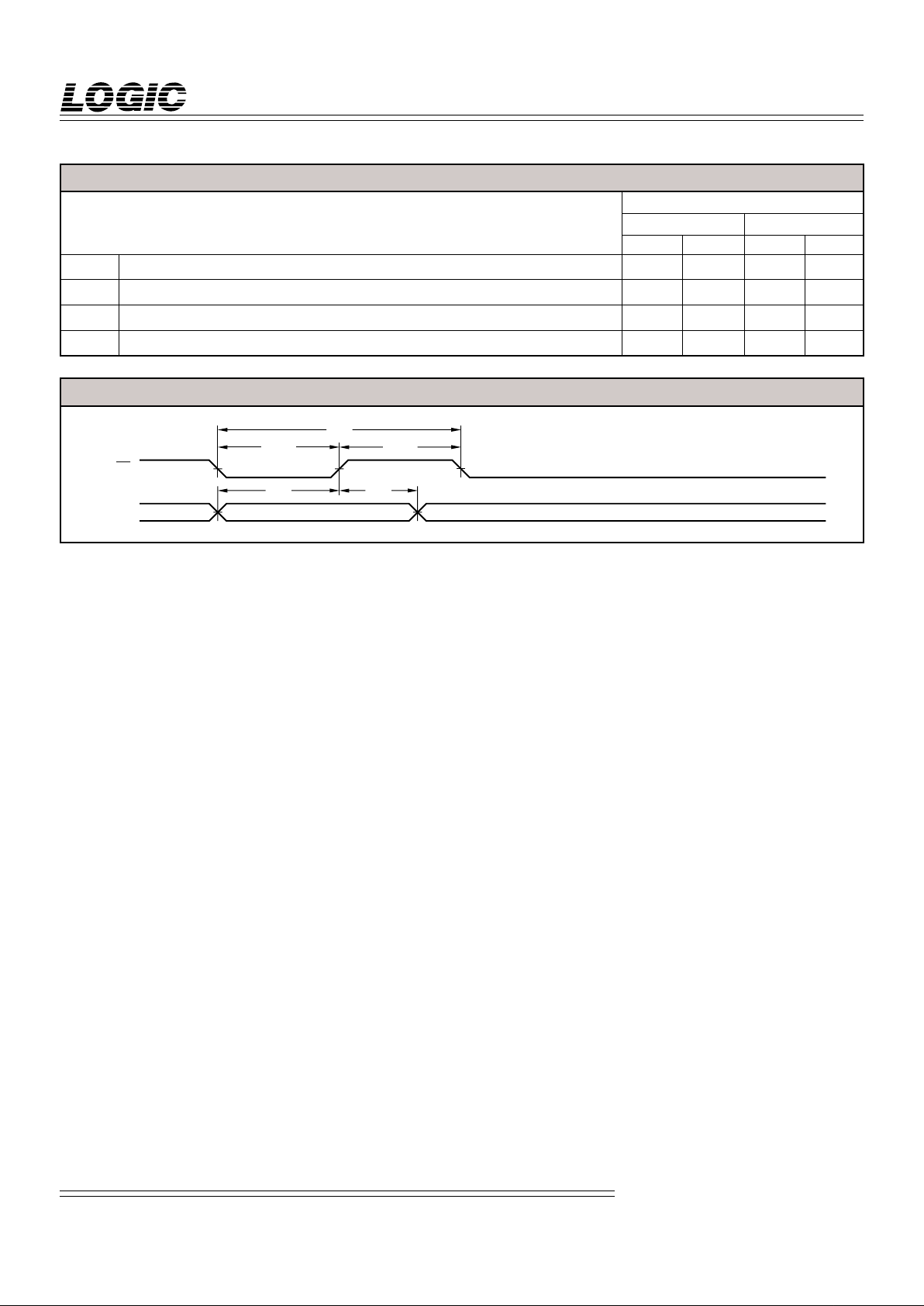
SWITCHING WAVEFORMS:DATA I/O
CLK
tCYC
tPW tPW
DINA11-0
DINB11-0
tS tH
DOUT12-0
α11-0
tS tH
CONTROLS*
tS tH
OE
tD
tDIS tENA
HIGH IMPEDANCE
*includes MIXEN, TC, and RND1-0.
DEVICES INCORPORATED
LF48212
12 x 12-bit Alpha Mixer
6
Video Imaging Products
08/16/2000–LDS.48212-F
LF48212–
25 20
Symbol Parameter Min Max Min Max
tLC LD Cycle Time 25 20
tLPW LD Pulse Width 10 10
tDS DEL Setup Time 12 12
tDH DEL Hold Time 0 0
COMMERCIAL OPERATING RANGE (0°C to +70°C)
Notes 9, 10 (ns)
SWITCHING WAVEFORMS:DELAY CONTROL REGISTER DATA
LD
t
LC
t
LPW
t
LPW
DEL
t
DS
t
DH

DEVICES INCORPORATED
Video Imaging Products
7
LF48212
12 x 12-bit Alpha Mixer
08/16/2000–LDS.48212-F
1. Maximum Ratings indicate stress
specifications only. Functional operation of these products at values beyond
those indicated in the Operating Conditions table is not implied. Exposure to
maximum rating conditions for extended periods may affect reliability.
2. The products described by this specification include internal circuitry designed to protect the chip from damaging substrate injection currents and accumulations of static charge. Nevertheless, conventional precautions should
be observed during storage, handling,
and use of these circuits in order to
avoid exposure to excessive electrical
stress values.
3. This device provides hard clamping of
transient undershoot and overshoot. Input levels below ground or above VCC
will be clamped beginning at –0.6 V and
VCC + 0.6 V. The device can withstand
indefinite operation with inputs in the
range of –0.5 V to +7.0 V. Device operation will not be adversely affected, however, input current levels will be well in
excess of 100 mA.
4. Actual test conditions may vary from
those designated but operation is guaranteed as specified.
5. Supply current for a given application can be accurately approximated by:
where
N = total number of device outputs
C = capacitive load per output
V = supply voltage
F = clock frequency
6. Tested with all outputs changing every cycle and no load, at a 40 MHz clock
rate.
7. Tested with all inputs within 0.1 V of
VCC or Ground, no load.
8. These parameters are guaranteed
but not 100% tested.
NCV F
4
2
NOTES
9. AC specifications are tested with
input transition times less than 3 ns,
output reference levels of 1.5 V (except
tDIS test), and input levels of nominally
0 to 3.0 V. Output loading may be a
resistive divider which provides for
specified IOH and IOL at an output
voltage of VOH min and VOL max
respectively. Alternatively, a diode
bridge with upper and lower current
sources of IOH and IOL respectively,
and a balancing voltage of 1.5 V may be
used. Parasitic capacitance is 30 pF
minimum, and may be distributed.
This device has high-speed outputs capable of large instantaneous current
pulses and fast turn-on/turn-off times.
As a result, care must be exercised in the
testing of this device. The following
measures are recommended:
a. A 0.1 µF ceramic capacitor should be
installed between VCC and Ground
leads as close to the Device Under Test
(DUT) as possible. Similar capacitors
should be installed between device VCC
and the tester common, and device
ground and tester common.
b. Ground and VCC supply planes
must be brought directly to the DUT
socket or contactor fingers.
c. Input voltages should be adjusted to
compensate for inductive ground and VCC
noise to maintain required DUT input
levels relative to the DUT ground pin.
10. Each parameter is shown as a minimum or maximum value. Input requirements are specified from the point
of view of the external system driving
the chip. Setup time, for example, is
specified as a minimum since the external system must supply at least that
much time to meet the worst-case requirements of all parts. Responses from
the internal circuitry are specified from
the point of view of the device. Output
delay, for example, is specified as a
maximum since worst-case operation of
any device always provides data within
that time.
11. For the tENA test, the transition is
measured to the 1.5 V crossing point
with datasheet loads. For the tDIS test,
the transition is measured to the
±200mV level from the measured
steady-state output voltage with
±10mA loads. The balancing voltage, VTH, is set at 3.5 V for Z-to-0
and 0-to-Z tests, and set at 0 V for Zto-1 and 1-to-Z tests.
12. These parameters are only tested at
the high temperature extreme, which is
the worst case for leakage current.
S1
I
OH
I
OL
V
TH
C
L
DUT
OE
0.2 V
t
DIS
t
ENA
0.2 V
1.5 V 1.5 V
3.5V Vth
1
Z
0
Z
Z
1
Z
0
1.5 V
1.5 V
0V Vth
VOL*
V
OH
*
V
OL
*
V
OH
*
Measured V
OL
with IOH = –10mA and IOL = 10mA
Measured V
OH
with IOH = –10mA and IOL = 10mA
FIGURE B. THRESHOLD LEVELS
FIGURE A. OUTPUT LOADING CIRCUIT

DEVICES INCORPORATED
LF48212
12 x 12-bit Alpha Mixer
8
Video Imaging Products
08/16/2000–LDS.48212-F
Plastic J-Lead Chip Carrier
(J2)
LF48212JC25
LF48212JC20
ORDERING INFORMATION
0°C to +70°C — COMMERCIAL SCREENING
Speed
25 ns
20 ns
68-pin
1234567
60
59
58
57
56
55
54
53
52
51
50
49
48
47
46
45
44
68 67 66 65 64 63
3635 37 38 39 413029 31 32 33 34
10
11
12
13
14
15
16
17
18
19
20
21
22
23
24
25
26
40
Top
View
896261
2827 42 43
DINB
11
DINB
10
DINB
9
DINB
8
DINB
7
DINB
6
GND
DINB
5
NC
DINB
4
DINB
3
DINB
2
DINB
1
DINB
0
RND
1
RND
0
DEL
OE
DOUT
12
DOUT
11
DOUT
10
DOUT
9
GND
DOUT
8
DOUT
7
NC
DOUT
6
DOUT
5
V
CC
DOUT
4
DOUT
3
DOUT
2
DOUT
1
DOUT
0
LD
TC
DINA
11
DINA
10
DINA
9
V
CC
DINA8DINA
7
NC
DINA
6
DINA5DINA
4
GND
DINA
3
DINA2DINA1DINA
0
CLK
MIXEN
α0α1α2α3α4
α5NCα6
α7
V
CC
α8α9α10
α11
BYPASS

DEVICES INCORPORATED
Video Imaging Products
9
LF48212
12 x 12-bit Alpha Mixer
08/16/2000–LDS.48212-F
Plastic Quad Flatpack
(Q3)
LF48212QC25
LF48212QC20
ORDERING INFORMATION
0°C to +70°C — COMMERCIAL SCREENING
Speed
25 ns
20 ns
64-pin
DINB
11
DINB
10
DINB
9
DINB
8
DINB
7
DINB
6
GND
DINB
5
DINB
4
DINB
3
DINB
2
DINB
1
DINB
0
RND
1
RND
0
DEL
CLK
MIXEN
α0α1α2α3α4α5α6α
7
V
CC
α8α9α10α
11
BYPASS
OE
DOUT
12
DOUT
11
DOUT
10
DOUT
9
GND
DOUT
8
DOUT
7
DOUT
6
DOUT
5
V
CC
DOUT
4
DOUT
3
DOUT
2
DOUT
1
DOUT
0
LD
TC
DINA
11
DINA
10
DINA
9
V
CC
DINA8DINA7DINA6DINA5DINA
4
GND
DINA
3
DINA2DINA1DINA
0
48
47
46
45
44
43
42
41
40
39
38
37
36
35
34
33
Top
View
1
2
3
4
5
6
7
8
9
10
11
12
13
14
15
16
171819202122232425262728293031
32
646362616059585756555453525150
49
 Loading...