DEVICES INCORPORATED
LF43891
9 x 9-bit Digital Filter
LF43891
DEVICES INCORPORATED
FEATURES DESCRIPTION
❑❑
❑ 30 MHz Maximum Sampling Rate
❑❑
❑❑
❑ 320 MHz Multiply-Accumulate Rate
❑❑
❑❑
❑ 8 Filter Cells
❑❑
❑❑
❑ 8-bit Unsigned or 9-bit Two’s
❑❑
Complement Data/Coefficients
❑❑
❑ 26-bit Data Outputs
❑❑
❑❑
❑ Shift-and-Add Output Stage for
❑❑
Combining Filter Outputs
❑❑
❑ Expandable Data Size, Coefficient
❑❑
Size, and Filter Length
❑❑
❑ User-Selectable 2:1, 3:1, or 4:1
❑❑
Decimation
❑❑
❑ Replaces Harris HSP43891
❑❑
❑❑
❑ 84-pin PLCC, J-Lead
❑❑
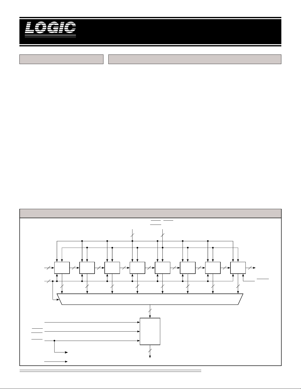
The LF43891 is a video-speed digital
filter that contains eight filter cells
(taps) cascaded internally and a shiftand-add output stage. A 9 x 9 multiplier, three decimation registers, and a
26-bit accumulator are contained in
each filter cell. The output stage of the
LF43891 contains a 26-bit accumulator
which can add the contents of any
filter stage to the output stage accumulator shifted right by 8 bits. 8-bit
unsigned or 9-bit two’s complement
format for data and coefficients can be
independently selected.
Expanded coefficients and word sizes
can be processed by cascading multiple LF43891s to implement larger
filter lengths without affecting the
sample rate. By reducing the sample
9 x 9-bit Digital Filter
rate, a single LF43891 can process
larger filter lengths by using multiple
passes. The sampling rate can range
from 0 to 40 MHz. Over 1000 taps
may be processed without overflows
due to the architecture of the device.
The output sample rate can be reduced to one-half, one-third, or onefourth the input sample rate by using
the three decimation registers contained in every filter cell. Matrix
multiplication, N x N spatial correlations/convolutions, and other 2-D
operations for image processing can
also be achieved using these registers.
LF43891 BLOCK DIAGRAM
CIN
8-0
ADR
2-0
SHADD
SENBL
SENBH
RESET
9
3
FILTER
CELL 0
9
FILTER
CELL 1
TO ALL CELLS
DIN
8-0
9
9 9
FILTER
CELL 2
2626 26 26 26 26 26 26
FILTER
CELL 3
DIENB, CIENB,
ERASE, DCM
9
MUX
26
OUTPUT
STAGE
26
5
FILTER
CELL 4
1-0
9
FILTER
CELL 5
9
FILTER
CELL 6
9
FILTER
CELL 7
9
COUT
COENB
8-0
SUM
TO ALL REGISTERSCLK
25-0
Video Imaging Products
1
08/16/2000–LDS.43891-J

DEVICES INCORPORATED
)
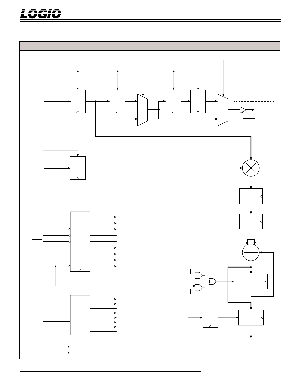
FIGURE 1. FILTER CELL DIAGRAM
LF43891
9 x 9-bit Digital Filter
DCM0.D DCM1.DCIENB.D
CIN8-0
DIENB.D
DIN8-0
DCM1
DCM0
RESET
DIENB
CIENB
ADR
ADR1
ADR2
ERASE
LD
C
C REG
LD
X REG
LATCHES
0
8-0
LD
D1 REG
DCM1.D
DCM
RESET.D
DIENB.D
CIENB.D
ADR
ADR
ADR
ERASE.D
0.D
0.D
1.D
2.D
LD
1
MUX
0
D2 REG
RESET.D
ERASE.D
D8-0
C8-0
X8-0
LD
D3 REG
1
MUX
0
SIGN EXTENSION
TRI-STATE BUFFER
ON FILTER CELL 7 ONLY
COUT8-0
COENB
M REG0
M REG1
25-18
ACC25-0
ACCUMULATOR
17-0
CELL 0
CELL 1
ADR0
ADR1
ADR2
CLK TO ALL REGISTERS
RESET.D TO ALL REGISTERS (EXCEPT ACCUMULATOR AND T-REGISTER
DECODER
CELL 2
CELL 3
CELL 4
CELL 5
CELL 6
CELL 7
2
CELL n
CELL n
ACC.D25-0
DQ
LD
T REG
AOUT
25-0
Video Imaging Products
08/16/2000–LDS.43891-J

DEVICES INCORPORATED
LF43891
9 x 9-bit Digital Filter
FILTER CELL DESCRIPTION
9-bit coefficients are loaded into the
C register (CIN8-0) and are output as
COUT8-0 (the COENB signal enables
the COUT8-0 outputs). The path
taken by the coefficients varies
according to the decimation mode
chosen. With no decimation, the
coefficients move directly from the
C register, bypassing all decimation
registers, and are available at the
output on the following clock cycle.
When decimation is chosen, the
coefficient output is delayed by 1, 2,
or 3 clock cycles depending on how
many decimation registers the
coefficients pass through (D1, D2, or
D3). The number of decimation
registers the coefficients pass
through is determined by DCM1-0.
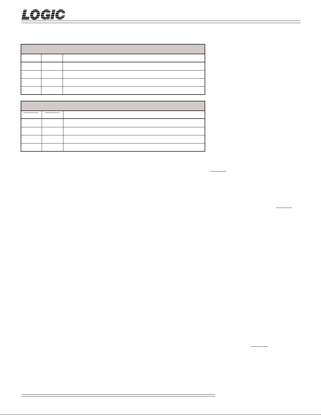
Refer to Table 1 for choosing a
decimation mode.
CIENB enables the C and D registers
for coefficient loading. The registers
are loaded on the rising edge of CLK
when CIENB is LOW. CIENB is
latched and delayed internally which
enables the registers for loading one
clock cycle after CIENB goes active
(loading takes place on the second
rising edge of CLK after CIENB goes
LOW). Therefore, CIENB must be
LOW one clock cycle before the
coefficients are placed on the CIN8-0
inputs. The coefficients are held when
CIENB is HIGH.
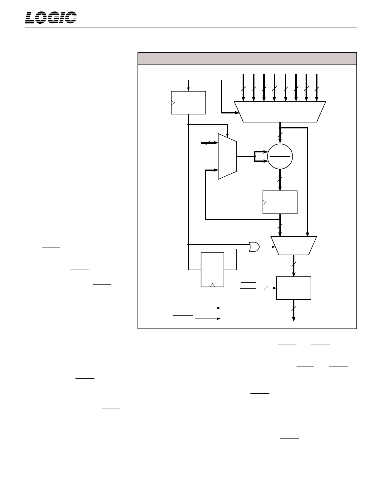
FIGURE 2. OUTPUT STAGE DIAGRAM
SHADD
D
Q
CLK
RESET.D
ADR
18
0
DQ
2-0
.D
26 26 26
01
EXTENSION
17-0
MUX
ZERO
25-8
SENBL
SENBH
TO ALL REGISTERS
TO ALL REGISTERS
CELL RESULT
SIGN
25-18
17-0
OUTPUT
BUFFER
2
MUX
26
26
26
OUTPUT
TRI-STATE
BUFFER
2626262626
01
MUX
26
26
DIENB enables the X register for the
loading of data. The X register is
loaded on the rising edge of CLK
when DIENB is LOW. DIENB is
latched and delayed internally (loading takes place on the second rising
edge of CLK after DIENB goes LOW).
Therefore, DIENB must be LOW one
clock cycle before the data is placed on
the DIN8-0 inputs. The X register is
loaded with all zeros when DIENB is
HIGH.
The output of the C register (C8-0) and
X register (X8-0) provide the inputs of
the 9 x 9 multiplier. The multiplier is
followed by two pipeline registers,
M REG0 and M REG1. The output of
the multiplier is sign extended and is
used as one of the inputs to the 26-bit
adder. The output of the 26-bit
accumulator provides the second
input to the adder. Both the accumulator and T register are loaded simultaneously with the output of the
adder.
The accumulator is loaded with the
output of the adder on every clock
cycle unless cleared. Clearing the
accumulator can be achieved using
two methods. The first method, when
both RESET and ERASE are LOW,
causes all accumulators and all
3
registers in the device to be cleared
together. RESET and ERASE are
latched and delayed internally causing the clearing to occur on the second
clock cycle after RESET and ERASE go
active.
The second method, when only
ERASE is LOW, clears a single accumulator of a selected cell. The cell is
selected using the ADR2-0 inputs
(decoded to Cell n). ERASE is latched
and delayed internally causing the
clearing to occur on the second clock
cycle after ERASE goes active. Refer
to Table 2 for clearing registers and
accumulators.
Video Imaging Products
08/16/2000–LDS.43891-J

DEVICES INCORPORATED
LF43891
9 x 9-bit Digital Filter
TABLE 1. DECIMATION MODE SELECTION
DCM1 DCM0 Decimation Function
0 0 Decimation registers not used
0 1 One decimation register used (decimation by one-half)
1 0 Two decimation registers used (decimation by one-third)
1 1 Three decimation registers used (decimation by one-fourth)
TABLE 2. REGISTER AND ACCUMULATOR CLEARING
ERASE RESET Clearing Effect
0 0 All accumulators and all registers are cleared
0 1 Only the accumulator addressed by ADR2-0 is cleared
1 0 All registers are cleared (accumulators are not cleared)
1 1 No clearing occurs, internal state remains the same
OUTPUT STAGE DESCRIPTION
The 26-bit adder contained in the
output stage can add the contents of
any filter cell accumulator (selected by
ADR2-0) with the 18 most significant
bits of the output buffer. The result is
stored back into the output buffer.
The complete operation takes only one
clock cycle. The eight least significant
bits of the output buffer are lost.
The Zero multiplexer is controlled by
the SHADD input signal. This allows
selection of either the 18 most significant bits of the output buffer or all
zeros for the adder input. When
SHADD is LOW, all zeros will be
selected. When SHADD is HIGH, the
18 most significant bits of the output
buffer are selected enabling the shiftand-add operation. SHADD is
latched and delayed internally by one
clock cycle.
The output multiplexer is also controlled by the SHADD input signal.
This allows selection of either a filter
cell accumulator, selected by ADR2-0,
or the output buffer to be output to
the SUM25-0 bus. Only the 26 least
significant bits from either a filter cell
accumulator or the output buffer are
output on SUM25-0. If SHADD is
LOW during two consecutive clock
cycles (low during the current and
previous clock cycle), the output
multiplexer selects the contents of a
filter cell accumulator addressed by
ADR2-0. Otherwise, the output
multiplexer selects the contents of the
output buffer.
If the same address remains on the
ADR2-0 inputs for more than one clock
cycle, SUM25-0 will not change to
reflect any updates to the addressed
cell accumulator. Only the result from
the first selection of the cell (first clock
cycle) will be output. This allows the
interface of slow memory devices
where the output needs to be active
for more than one clock cycle. Normal
FIR operation is not affected because
ADR2-0 is changed sequentially.
NUMBER SYSTEMS
Data and coefficients can be represented as either 8-bit unsigned or 9-bit
two's complement numbers. All
values are represented as 9-bit two's
complement numbers internally. If
the most significant or sign bit is a
zero, the multiplier can multiply 8-bit
unsigned numbers.
SIGNAL DEFINITIONS
Power
VCC and GND
+5 V power supply. All pins must be
connected.
Clock
CLK — Master Clock
The rising edge of CLK strobes all
registers. All timing specifications are
referenced to the rising edge of CLK.
Inputs
DIN8-0 — Data Input
9-bit data is latched into the X register
of each filter cell simultaneously. The
DIENB signal enables loading of the
data.
CIN8-0 — Coefficient Input
9-bit coefficients are latched into the C
register of Filter Cell 0. The CIENB
signal enables loading of the coefficients.
Outputs
SUM25-0 — Data Output
The 26-bit result from an individual
filter cell will appear when ADR2-0 is
used to select the filter cell result.
SHADD in conjunction with ADR2-0 is
used to select the output from the
shift-and-add output stage.
COUT8-0 — Coefficient Output
The 9-bit coefficient output from
Filter Cell 7 can be connected to the
CIN8-0 coefficient input of the same
LF43891 to recirculate the coefficients.
COUT8-0 can also be connected to the
CIN8-0 of another LF43891 to cascade
the devices. The COENB signal
enables the output of the coefficients.
Video Imaging Products
4
08/16/2000–LDS.43891-J
 Loading...