LOGIC LF43168QC30, LF43168QC22, LF43168JC30, LF43168JC22, LF43168JC15 Datasheet
...
DEVICES INCORPORATED
Video Imaging Products
1
LF43168
Dual 8-Tap FIR Filter
03/28/2000–LDS.43168-H
❑❑
❑❑
❑ 66 MHz Data and Computation Rate
❑❑
❑❑
❑ Two Independent 8-Tap or Single
16-Tap FIR Filters
❑❑
❑❑
❑ 10-bit Data and Coefficient Inputs
❑❑
❑❑
❑ 32 Programmable Coefficient Sets
❑❑
❑❑
❑ Supports Interleaved Coefficient Sets
❑❑
❑❑
❑ User Programmable Decimation up
to 16:1
❑❑
❑❑
❑ Maximum of 256 FIR Filter Taps,
16 x 16 2-D Kernels, or 10 x 20-bit
Data and Coefficients
❑❑
❑❑
❑ Replaces Harris HSP43168
❑❑
❑❑
❑ Package Styles Available:
• 84-pin Plastic LCC, J-Lead
• 100-pin Plastic Quad Flatpack
FEATURES DESCRIPTION
LF43168
Dual 8-Tap FIR Filter
DEVICES INCORPORATED
The LF43168 is a high-speed dual FIR
filter capable of filtering data at realtime video rates. The device contains
two FIR filters which may be used as
two separate filters or cascaded to
form one filter. The input and coefficient data are both 10-bits and can be
in unsigned, two’s complement, or
mixed mode format.
The filter architecture is optimized for
symmetric coefficient sets. When
symmetric coefficient sets are used,
each filter can be configured as an 8-tap
FIR filter. If the two filters are cascaded, a 16-tap FIR filter can be
implemented. When asymmetric
coefficient sets are used, each filter is
configured as a 4-tap FIR filter. If both
filters are cascaded, an 8-tap filter can
be implemented. The LF43168 can
decimate the output data by as much
as 16:1. When the device is programmed to decimate, the number of
clock cycles available to calculate filter
taps increases. When configured for
16:1 decimation, each filter can be
configured as a 128-tap FIR filter (if
symmetric coefficient sets are used).
By cascading these two filters, the
device can be configured as a 256-tap
FIR filter.
There is on-chip storage for 32
different sets of coefficients. Each set
consists of eight coefficients. Access
to more than one coefficient set
facilitates adaptive filtering operations. The 28-bit filter output can be
rounded from 8 to 19 bits.
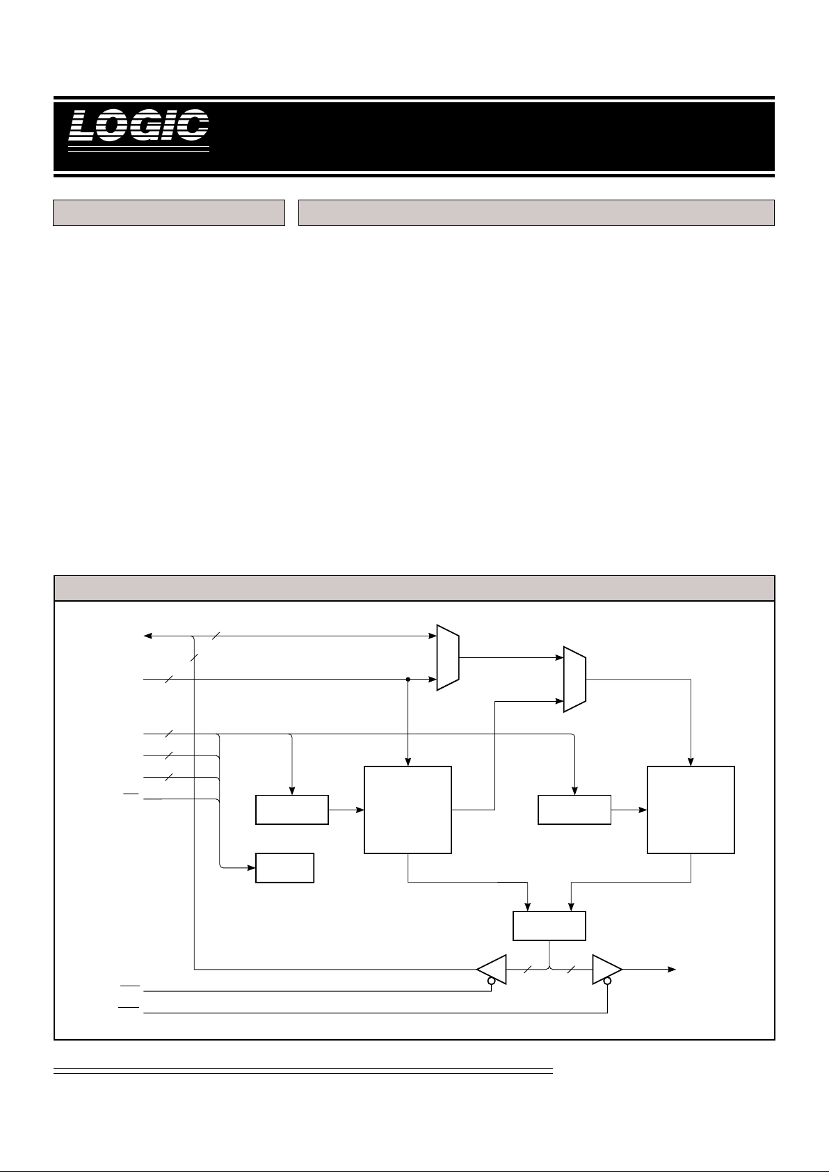
LF43168 BLOCK DIAGRAM
CIN
9-0
A
8-0
WR
CONTROL
10
9
CSEL
4-0
5
COEFFICIENT
BANK A
COEFFICIENT
BANK B
FILTER
CELL A
FILTER
CELL B
MUX
INA
9-0
INB
9-0
/
OUT
8-0
MUX/ADDER
9
19
MUX
OEL
OEH
OUT
27-9
10
10
9
DEVICES INCORPORATED
LF43168
Dual 8-Tap FIR Filter
2
Video Imaging Products
03/28/2000–LDS.43168-H
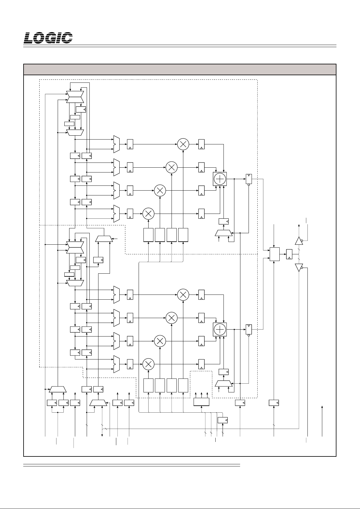
FIGURE 1. LF43168 FUNCTIONAL BLOCK DIAGRAM
TXFR
4
3
MUX
3
3
3
SHFTEN
INA
9-0
MUX
INB9-0/
OUT8-0
10
MUX_CTRL
TO ALL
DECIMATION
REGISTERS
CIN
9-0
A8-0
WR
CONTROL
COEF
BANK 0
COEF
BANK 1
COEF
BANK 2
COEF
BANK 3
3
FWRD
RVRS
TO ALL
ALUs
TO ALL
ALUs
ODD/EVEN
(TO ALL ALUs)
MUX_CTRL
ROUND_CTRL
3
ALU
1-16
1-16
1-16
1-16
1-16
1-16
MUX
0
MUX
MUX
DEMUX
10
9
1-16
MUX
MUX_CTRL
1-16
1-16
1-16
1-16
1-16
1-16
MUX
LIFO A
COEF
BANK 0
COEF
BANK 1
COEF
BANK 2
COEF
BANK 3
MUX
0
LIFO B
1-16
MUX
DEMUX
LIFO A
LIFO B
1-16
MUX_CTRL
5
ACCEN
MUX/
ADDER
ROUND_CTRL
6
MUX1-0
4
CSEL4-0
5
2
2
9 19
OUT27-9
OEL
OEH
CLK N data
CLK N+1 data
CLK N data
CLK N+1 data
10
AB
ALU
AB
ALU
AB
ALU
AB
ALU
AB
ALU
AB
ALU
AB
ALU
AB
FIR FILTER A FIR FILTER B
DECIMATION REGISTERS DECIMATION REGISTERS
NOTE: NUMBERS IN REGISTERS INDICATE NUMBER OF PIPELINE DELAYS.
CLK
9
DEVICES INCORPORATED
Video Imaging Products
3
LF43168
Dual 8-Tap FIR Filter
03/28/2000–LDS.43168-H
SIGNAL DEFINITIONS
Power
VCC and GND
+5 V power supply. All pins must be
connected.
Clock
CLK — Master Clock
The rising edge of CLK strobes all
enabled registers.
Inputs
INA9-0 — Data Input (FIR Filter A)
INA9-0 is the 10-bit registered data
input port for FIR Filter A. INA9-0
can also be used to send data to FIR
Filter B. Data is latched on the
rising edge of CLK.
INB9-0 — Data Input (FIR Filter B)
INB9-0 is the 10-bit registered data
input port for FIR Filter B. Data is
latched on the rising edge of CLK.
INB9-1 is also used as OUT8-0, the nine
least significant bits of the data output
port (see OUT27-0 section).
CIN9-0 — Coefficient/Control Data Input
CIN9-0 is the data input port for the
coefficient and control registers. Data
is latched on the rising edge of WR.
A8-0 — Coefficient/Control Address
A8-0 provides the write address for data
on CIN9-0. Data is latched on the
falling edge of WR.
WR — Coefficient/Control Write
The rising edge of WR latches data on
CIN9-0 into the coefficient/control
register addressed by A8-0.
CSEL4-0 — Coefficient Select
CSEL4-0 determines which set of
coefficients is sent to the multipliers in
both FIR filters. Data is latched on the
rising edge of CLK.
Outputs
OUT27-0 — Data Output
OUT27-0 is the 28-bit registered data
output port. OUT8-0 is also used as
INB9-1, the nine most significant bits
of the FIR Filter B data input port (see
INB9-0 section). If both filters are
configured for even-symmetric
coefficients, and both input and
coefficient data is unsigned, the filter
output data will be unsigned. Otherwise, the output data will be in two’s
complement format.
Controls
SHFTEN — Shift Enable
When SHFTEN is LOW, data on
INA9-0 and INB9-0 can be latched into
the device and data can be shifted
through the decimation registers.
When SHFTEN is HIGH, data on
INA9-0 and INB9-0 can not be latched
into the device and data in the input
and decimation registers is held. This
signal is latched on the rising edge
of CLK.
FWRD — Forward ALU Input
When FWRD is LOW, data from the
forward decimation path is sent to the
“A” inputs on the ALUs. When
FWRD is HIGH, “0” is sent to the “A”
inputs on the ALUs. This signal is
latched on the rising edge of CLK.
RVRS — Reverse ALU Input
When RVRS is LOW, data from the
reverse decimation path is sent to the
“B” inputs on the ALUs. When RVRS
is HIGH, “0” is sent to the “B” inputs
on the ALUs. This signal is latched on
the rising edge of CLK.
TXFR — LIFO Transfer Control
When TXFR goes LOW, the LIFO
sending data to the reverse decimation
path becomes the LIFO receiving data
from the forward decimation path,
and the LIFO receiving data from the
forward decimation path becomes the
LIFO sending data to the reverse
decimation path. The device must see
a HIGH to LOW transition of TXFR in
order to switch LIFOs. This signal is
latched on the rising edge of CLK.
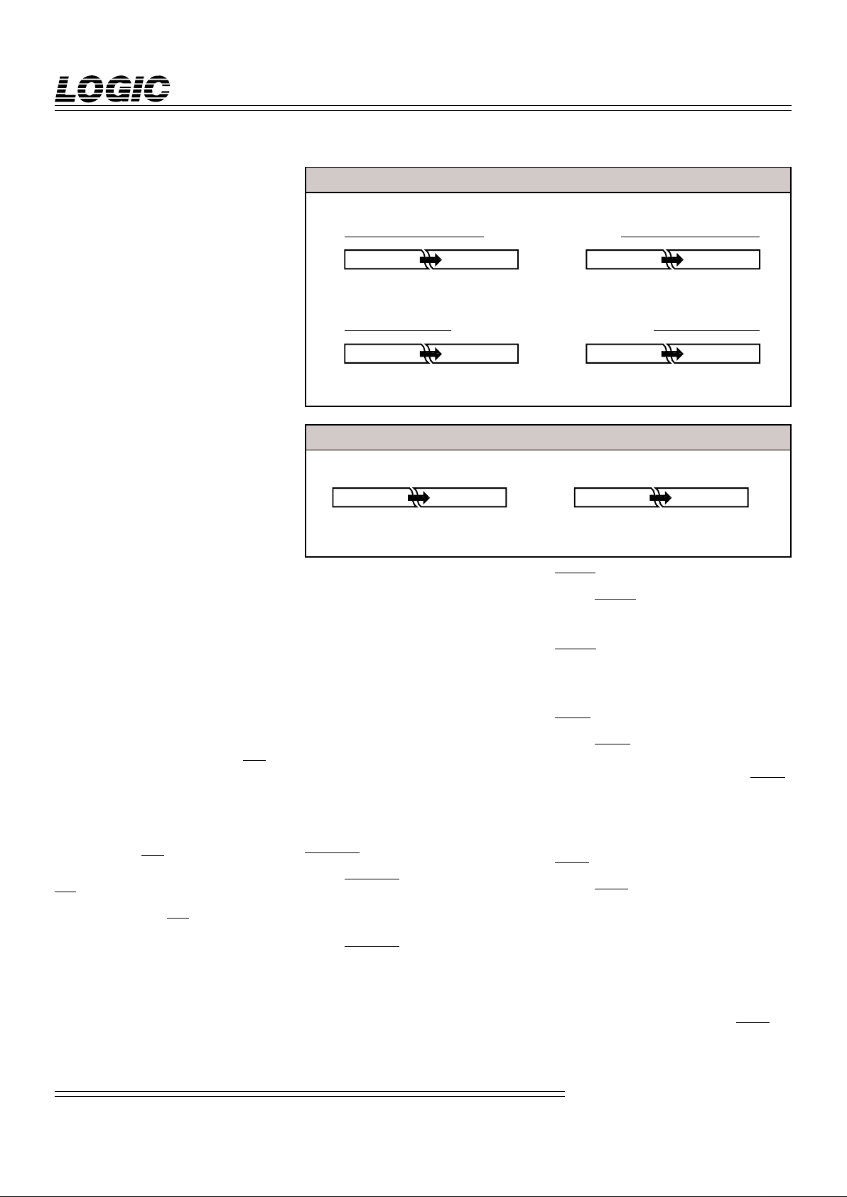
FIGURE 2A.INPUT FORMATS
987 210
2
02–12–2
2–72–82
–9
987 210
2
02–12–2
2–72–82
–9
987 210
–2
0
(Sign)
2–12
–2
2–72–82
–9
987 210
–2
0
(Sign)
2–12
–2
2–72–82
–9
Fractional Unsigned
Fractional Two's Complement
Data Coefficient
FIGURE 2B.OUTPUT FORMATS
27 26 25 2 1 0
2
92827
2
–162–172–18
27 26 25 2 1 0
–2
9
(Sign)
282
7
2
–162–172–18
Fractional Unsigned Fractional Two's Complement
DEVICES INCORPORATED
LF43168
Dual 8-Tap FIR Filter
4
Video Imaging Products
03/28/2000–LDS.43168-H
ACCEN — Accumulate Enable
When ACCEN is HIGH, both accumulators are enabled for accumulation
and writing to the accumulator output
registers is disabled (the registers hold
their values). When ACCEN goes
LOW, accumulation is halted (by
sending zeros to the accumulator
feedback inputs) and writing to the
accumulator output registers is
enabled. This signal is latched on the
rising edge of CLK.
MUX1-0 — Mux/Adder Control
MUX1-0 controls the Mux/Adder as
shown in Table 3. Data is latched on
the rising edge of CLK.
OEL — Output Enable Low
When OEL is LOW, OUT8-0 is enabled
for output and INB9-1 can not be used.
When OEL is HIGH, OUT8-0 is placed
in a high-impedance state and INB9-1
is available for data input.
OEH — Output Enable High
When OEH is LOW, OUT27-9 is
enabled for output. When OEH is
HIGH, OUT27-9 is placed in a highimpedance state.
FUNCTIONAL DESCRIPTION
Control Registers
There are two control registers which
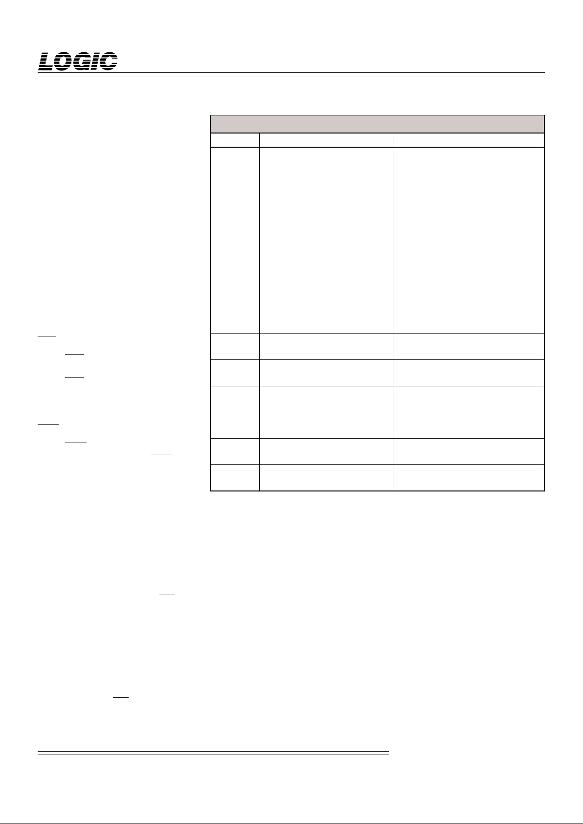
determine how the LF43168 is configured. Tables 1 and 2 show how each
register is organized. Data on CIN9-0
is latched into the addressed control
register on the rising edge of WR.
Address data is input on A8-0. Control Register 0 is written to using
address 000H. Control Register 1 is
written to using address 001H (Note
that addresses 002H to 0FFH are
reserved and should not be written
to). When a control register is written
to, a reset occurs which lasts for 6 CLK
cycles from when WR goes HIGH.
This reset does not alter any data in
the coefficient banks. Control data
can be loaded asynchronously to CLK.
Bits 0-3 of Control Register 0 control
the decimation registers. The decimation factor and decimation register
delay length is set using these bits.
Bit 4 determines if FIR filters A and B
operate separately as two filters or
together as one filter. Bit 5 is used to
select even or odd-symmetric coefficients. Bits 6 and 7 determine if there
are an even or odd number of taps in
filters A and B respectively. When the
FIR filters are set to operate as two
separate filters, bit 8 selects either
INA9-0 or INB9-0 as the filter B input
source. Bit 9 determines if the coefficient set used is interleaved or noninterleaved (see Interleaved Coefficient Filters section). Most applications use non-interleaved coefficient
sets (bit 9 set to “0”).
Bits 0 and 1 of Control Register 1
determine the input and coefficient
data formats respectively for filter A.
Bits 2 and 3 determine the input and
coefficient data formats respectively
for filter B. Bit 4 is used to enable or
disable data reversal on the reverse
decimation path. When data reversal
is enabled, the data order is reversed
before being sent to the reverse
decimation path. Bits 5-8 select where
rounding will occur on the output
data (See Mux/Adder section). Bit 9
enables or disables output rounding.
Coefficient Banks
The coefficient banks supply coefficient data to the multipliers in both
FIR filters. The LF43168 can store 32
different coefficient sets. A coefficient
BITS FUNCTION DESCRIPTION
0–3 Decimation Factor/ 0000 = No Decimation, Delay by 1
Decimation Register Delay Length 0001 = Decimate by 2, Delay by 2
0010 = Decimate by 3, Delay by 3
0011 = Decimate by 4, Delay by 4
0100 = Decimate by 5, Delay by 5
0101 = Decimate by 6, Delay by 6
0110 = Decimate by 7, Delay by 7
0111 = Decimate by 8, Delay by 8
1000 = Decimate by 9, Delay by 9
1001 = Decimate by 10, Delay by 10
1010 = Decimate by 11, Delay by 11
1011 = Decimate by 12, Delay by 12
1100 = Decimate by 13, Delay by 13
1101 = Decimate by 14, Delay by 14
1110 = Decimate by 15, Delay by 15
1111 = Decimate by 16, Delay by 16
4 Filter Mode Select 0 = Single Filter Mode
1 = Dual Filter Mode
5 Coefficient Symmetry Select 0 = Even-Symmetric Coefficients
1 = Odd-Symmetric Coefficients
6 FIR Filter A: Odd/Even Taps 0 = Odd Number of Filter Taps
1 = Even Number of Filter Taps
7 FIR Filter B: Odd/Even Taps 0 = Odd Number of Filter Taps
1 = Even Number of Filter Taps
8 FIR Filter B Input Source 0 = Input from INA9-0
1 = Input from INB9-0
9 Interleaved/Non-Interleaved 0 = Non-Interleaved Coefficient Sets
Coefficient Sets 1 = Interleaved Coefficient Sets
TABLE 1. CONTROL REGISTER 0 – ADDRESS 000H

DEVICES INCORPORATED
Video Imaging Products
5
LF43168
Dual 8-Tap FIR Filter
03/28/2000–LDS.43168-H
set consists of 8 coefficient values.
Each bank can hold 32 10-bit values.
CSEL4-0 is used to select which
coefficient set is sent to the filter
multipliers. The coefficient set fed to
the multipliers may be switched every
CLK cycle if desired.
Data on CIN9-0 is latched into the
addressed coefficient bank on the
rising edge of WR. Address data is
input on A8-0 and is decoded as
follows: A1-0 determines the bank
number (“00”, “01”, “10”, and “11”
correspond to banks 0, 1, 2, and 3
respectively), A2 determines which
filter (“0” = filter A, “1” = filter B), A7-3
determines which set number the
coefficient is in, and A8 must be set to
“1”. For example, an address of
“100111011” will load coefficient set 7
in bank 3 of filter A with data. Coefficient data can be loaded asynchronously to CLK.
Decimation Registers
The decimation registers are provided
to take advantage of symmetric filter
coefficients and to provide data
storage for 2-D filtering. The outputs
of the registers are fed into the ALUs.
Both inputs to an ALU need to be
multiplied by the same filter coefficient. By adding or subtracting the
two data inputs together before being
sent to the filter multiplier, the number of filter taps needed is cut in half.
Therefore, an 8-tap FIR filter can be
made with only four multipliers. The
decimation registers are divided into
two groups, the forward and reverse
decimation registers. As can be seen
in Figure 1, data flows left to right
through the forward decimation
registers and right to left through the
reverse decimation registers. The
decimation registers can be pro-
BITS FUNCTION DESCRIPTION
0 FIR Filter A Input Data Format 0 = Unsigned
1 = Two’s Complement
1 FIR Filter A Coefficient Format 0 = Unsigned
1 = Two’s Complement
2 FIR Filter B Input Data Format 0 = Unsigned
1 = Two’s Complement
3 FIR Filter B Coefficient Format 0 = Unsigned
1 = Two’s Complement
4 Data Order Reversal Enable 0 = Enabled
1 = Disabled
5–8 Output Round Position 0000 = 2
–10
0001 = 2
–9
0010 = 2
–8
0011 = 2
–7
0100 = 2
–6
0101 = 2
–5
0110 = 2
–4
0111 = 2
–3
1000 = 2
–2
1001 = 2
–1
1010 = 2
0
1011 = 2
1
9 Output Round Enable 0 = Enabled
1 = Disabled
TABLE 2. CONTROL REGISTER 1 – ADDRESS 001H
grammed to decimate by 2 to 16 (see
Decimation section and Table 1).
SHFTEN enables and disables the
shifting of data through the decimation registers. When SHFTEN is LOW,
data on INA9-0 and INB9-0 can be
latched into the device and data can
be shifted through the decimation
registers. When SHFTEN is HIGH,
data on INA9-0 and INB9-0 can not be
latched into the device and data in the
input and decimation registers is held.
Data feedback circuitry is positioned
between the forward and reverse
decimation registers. It controls how
data from the forward decimation
path is fed to the reverse decimation
path. The feedback circuitry can
either reverse the data order or pass
the data unchanged to the reverse
decimation path. The mux/demux
sends incoming data to one of the
LIFOs or the data feedback decimation
register. The LIFOs and decimation
register feed into a mux. This mux
determines if one of the LIFOs or the
decimation register sends data to the
reverse decimation path.
If the data order needs to be reversed
before being sent to the reverse
decimation path (for example, when
decimating), Data Reversal Mode
should be enabled by setting bit 4 of
Control Register 1 to “0”. When Data
Reversal is enabled, data from the
forward decimation path is written
into one of the LIFOs in the data
feedback section while the other LIFO
sends data to the reverse decimation
path. When TXFR goes LOW, the
LIFO sending data to the reverse
decimation path becomes the LIFO
receiving data from the forward
decimation path, and the LIFO
receiving data from the forward
decimation path becomes the LIFO
sending data to the reverse decimation
path. The device must see a HIGH to
LOW transition of TXFR in order to
switch LIFOs. The size of data blocks
sent to the reverse decimation path is
determined by how often TXFR goes
LOW. To send data blocks of size 8 to
 Loading...