DEVICES INCORPORATED
LF3370
High-Definition Video Format Converter
LF3370
DEVICES INCORPORATED
FEATURES
❑❑
❑ 83 MHz Data Rate for HDTV
❑❑
Applications
❑❑
❑ Supports Multiple Video Formats
❑❑
Bi-Directional Conversions:
- 4:2:2:4
- 4:4:4:4
- R/G/B/Key
- Y/U/V/Key
❑❑
❑ Multiplexed and Non-multiplexed
❑❑
I/O Data
❑❑
❑ User-Programmable:
❑❑
- 3 x 3 Colorspace Converter
- LUT for Gamma Correction
- I/O Bias Compensation
- Bypass Capability
❑❑
❑ 13-bit Data Path, Colorspace
❑❑
Converter Coefficients and Key
Channel Scaling Coefficients
❑❑
❑ 160-lead PQFP
❑❑
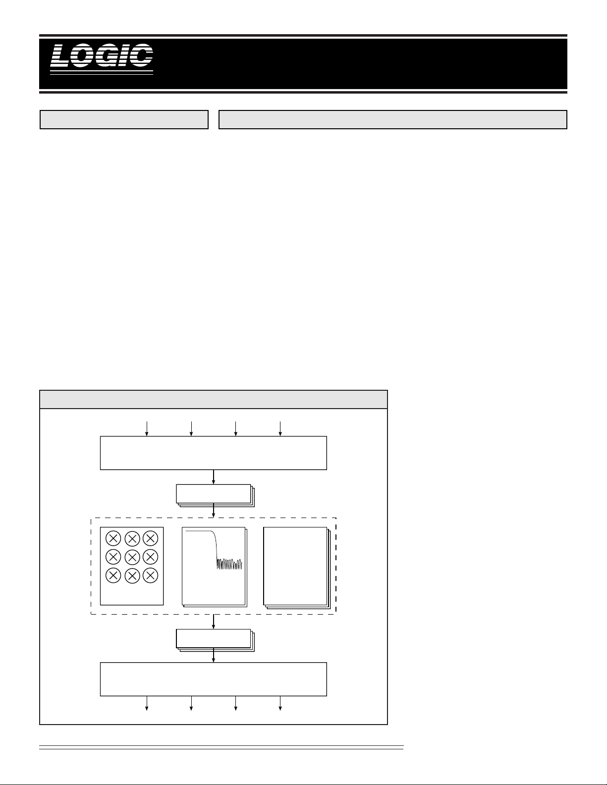
LF3370 BLOCK DIAGRAM
B
A
12-0
12-0
INPUT DE-MULTIPLEXER SECTION
INPUT BIAS ADDERS
High-Definition Video Format Converter
DESCRIPTION
The LF3370 is a video format
converter capable of operating at
HDTV data rates. This device
converts to and from any of the
various SDTV/HDTV digital video
formats by utilizing an internal
3 x 3 Matrix Multiplier and two
1:2 Interpolation/2:1 Decimation
Half-Band Filters.
Using the Input Demultiplexer
and Output Multiplexer, the
LF3370 can accept and output
interleaved or non-interleaved
video. For example, R/G/B/Key
data can be color space converted
to Y/U/V/Key and down-converted to 4:2:2:4. By re-arranging
the order of the functional sections, the opposite conversion can
be achieved. The coefficients for
C
12-0
D
12-0
the 3 x 3 Matrix Multiplier are
fully user programmable to support a wide range of color space
conversions. The two Interpolation/Decimation Half-Band Filters
are fully compliant with SMPTE
260M.
Input and Output Bias Adders are
included for removing or adding a
user-defined bias into the video
signal. In addition, three programmable 1K x 13-bit Look-Up
Tables (LUTs) have also been
included for various uses such as
gamma correction. A Scaler has
been included on the Key Channel
for scaling to a desired magnitude
using user programmable coefficients.
Input signals can also be forced to
user-defined levels for horizontal
blanking. Furthermore, Round/
Select/Limit (RSL) circuitry is
provided at the end of various
stages to provide the best possible
conversions without color violations. For additional flexibility,
the Halfband Filter can be individually bypassed using an internal programmable length delay.
All control and coefficient registers
are loaded through the LF Interface™.
COLORSPACE
CONVERTER/
KEY SCALER
W
12-0
55-TAP HALF-BAND
INTERPOLATION/
DECIMATION
FILTERS
OUTPUT BIAS ADDERS
OUTPUT MULTIPLEXER SECTION
X
12-0
Y
12-0
1K x 13-Bit
LOOK-UP-TABLES
Z
12-0
1
This device operates at 3.3 V (5 V
tolerant I/O) and is available in
160-lead PQFP package.
Video Imaging Products
03/13/2001–LDS.3370-F
DEVICES INCORPORATED
High-Definition Video Format Converter
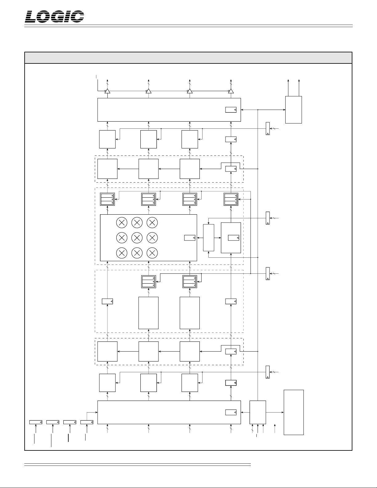
FIGURE 1. LF3370 FUNCTIONAL BLOCK DIAGRAM (HALF-BAND FILTER TO COLORSPACE ARRANGEMENT)
12-0
OE
WOUT
13
12-0
XOUT
13
12-0
YOUT
13
12-0
ZOUT
13
HF0HF
1
LF3370
13
BIAS
ADDER
OUTPUT
13
LUT*
1K x 13-bit
13
LIMIT
SELECT
ROUND
20
3 X 3 MATRIX MULTIPLY / KEY SCALER
35
13
BIAS
ADDER
OUTPUT
13
LUT*
1K x 13-bit
LIMIT
SELECT
ROUND
20 13
LIMIT
SELECT
ROUND
20 13
MUX
OUTPUT
CONVERTER
COLORSPACE
13
BIAS
ADDER
OUTPUT
13
LUT*
1K x 13-bit
LIMIT
SELECT
ROUND
20 13
3
LIMIT
SELECT
ROUND
20 13
BANKS 0-9
KEY SCALER
COEFFICIENT
23-5
13
1
13
2
13
LIMIT
SELECT
ROUND
20
3
13
35
FLAG
GENERATOR
1-0
OUTBIAS
1-0
2 2
CA
1-0
2
RSL
HBLANK
DATAPASS
RESET
CHROMA HALF-BAND FILTER / INTERPOLATOR
13
LUT*
1K x 13-bit
INPUT LOOK-UP-TABLE* OUTPUT LOOK-UP-TABLE*
13
BIAS
INPUT
ADDER
13 13
13
SYNC
12-0
AIN
FILTER/
HALF-BAND
INTERPOLATOR
13
LUT*
1K x 13-bit
13
BIAS
INPUT
ADDER
13
13
12-0
BIN
INPUT
DEMUX
FILTER/
HALF-BAND
INTERPOLATOR
13
LUT*
1K x 13-bit
13
BIAS
INPUT
ADDER
13
13
12-0
CIN
2
13
2
13
1
13
1-0
2
INBIAS
LF
INTERFACE
13
12-0
DIN
13
LD
12-0
CF
PAUSE
CONFIGURATION AND
CLK
CONTROL REGISTERS
TO NUMBER OF PIPELINE DELAYS THROUGH THAT PARTICULAR FUNCTIONAL BLOCK
THE LOOK-UP-TABLE IS TWO REGARDLESS OF WHETHER IT IS USED OR NOT.
* UP TO ONE LOOK-UP-TABLE MAY BE USED PER DATA PATH. THE INHERENT DELAY THROUGH
NOTE: NUMBERS IN REGISTERS INDICATE NUMBER OF PIPELINE DELAYS WHICH IS ALSO EQUIVALENT
Video Imaging Products
03/13/2001–LDS.3370-F
DEVICES INCORPORATED
High-Definition Video Format Converter
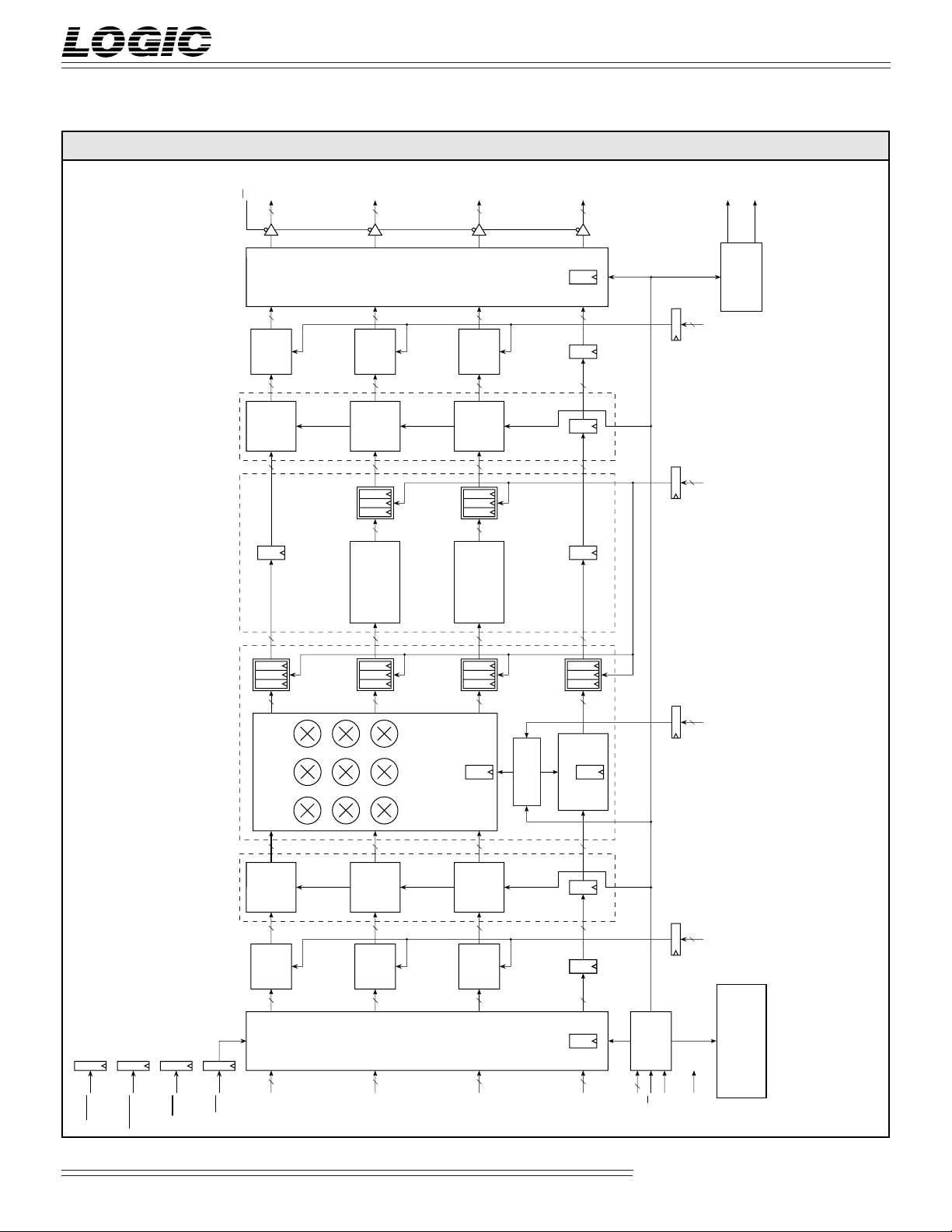
FIGURE 2. LF3370 FUNCTIONAL BLOCK DIAGRAM (COLORSPACE TO HALF-BAND FILTER ARRANGEMENT)
12-0
OE
WOUT
13
12-0
XOUT
13
12-0
YOUT
13
12-0
ZOUT
13
HF0HF
1
LF3370
13
BIAS
ADDER
OUTPUT
13
LUT*
1K x 13-bit
13
35
HALF-BAND
CHROMA HALF-BAND FILTER / INTERPOLATOR
13
LIMIT
SELECT
ROUND
20
13
BIAS
ADDER
OUTPUT
13
LUT*
1K x 13-bit
13
LIMIT
SELECT
ROUND
20
FILTER/
DECIMATOR
13
LIMIT
SELECT
ROUND
20
MUX
OUTPUT
13
BIAS
ADDER
OUTPUT
13
LUT*
1K x 13-bit
13
LIMIT
SELECT
ROUND
20
FILTER/
HALF-BAND
DECIMATOR
13
LIMIT
SELECT
ROUND
20
23-5
13
1
13
2
13
35
13
LIMIT
SELECT
ROUND
20
FLAG
GENERATOR
1-0
2
OUTBIAS
1-0
2
RSL
1-0
2
CA
HBLANK
DATAPASS
RESET
3 X 3 MATRIX MULTIPLY / KEY SCALER
13
LUT*
1K x 13-bit
INPUT LOOK-UP-TABLE* OUTPUT LOOK-UP-TABLE*
13
BIAS
INPUT
ADDER
13
13
SYNC
12-0
AIN
13
LUT*
1K x 13-bit
13
BIAS
INPUT
ADDER
13
13
12-0
BIN
CONVERTER
COLORSPACE
INPUT
DEMUX
3
13
LUT*
1K x 13-bit
13
BIAS
INPUT
ADDER
13
13
12-0
CIN
3
BANKS 0-9
KEY SCALER
COEFFICIENT
3
13
2
13
1
13
1-0
2
INBIAS
LF
INTERFACE
13
12-0
DIN
13
LD
12-0
CF
PAUSE
CONFIGURATION AND
CLK
CONTROL REGISTERS
TO NUMBER OF PIPELINE DELAYS THROUGH THAT PARTICULAR FUNCTIONAL BLOCK
THE LOOK-UP-TABLE IS TWO REGARDLESS OF WHETHER IT IS USED OR NOT.
* UP TO ONE LOOK-UP-TABLE MAY BE USED PER DATA PATH. THE INHERENT DELAY THROUGH
NOTE: NUMBERS IN REGISTERS INDICATE NUMBER OF PIPELINE DELAYS WHICH IS ALSO EQUIVALENT
Video Imaging Products
03/13/2001–LDS.3370-F

DEVICES INCORPORATED
LF3370
High-Definition Video Format Converter
SIGNAL DEFINITIONS
Power
VCC and GND
+3.3 V power supply. All power pins
must be connected.
Clock
CLK — Master Clock
The rising edge of CLK strobes all
enabled registers. To guarantee data
integrity, a minimum of 25KHz must
be maintained.
Inputs
A12-0, B12-0, C12-0, D12-0 — Data Inputs
A12-0, B12-0, C12-0, and D12-0 are the
13-bit registered data input ports.
Data is latched on the rising edge of
CLK.
CF12-0 — Coefficient Input
CF12-0 is used to address and load
Colorspace/Key Scaler coefficient
banks, Round/Select/Limit registers,
and Configuration registers. Data
present on CF12-0 is latched into the
LF InterfaceTM on the rising edge of
CLK when LD is LOW.
CA1-0 — Coefficient Address
CA1-0 determines which of the four
user-programmable Colorspace/Key
Scaler Coefficients are used.
Outputs
W12-0 , X12-0 , Y12-0 , Z12-0 — Data Outputs
HF1/HF0 — HBlank Flags
HF1 and HF0 are two general purpose
flags used to indicate when a 20-bit
counter reaches its user-defined
terminal count; a HIGH to LOW
transition of HBLANK and/or RESET
will reset the flags.
Controls
LD — Configuration Load
When LD is LOW, data on CF12-0 is
latched into the LF3370 LF Interface
TM
on the rising edge of CLK. When LD
is HIGH, data is not loaded into
the LF InterfaceTM. When enabling
the LF InterfaceTM for data input, a
latched HIGH to LOW transition of
LD is required in order for the input
circuitry to function properly.
Therefore, LD must be set HIGH
immediately after power up to
ensure proper operation of the input
circuitry.
SYNC — Synchronization for data alignment
SYNC control signal is required to
properly synchronize the input
demultiplexer, output multiplexer,
and halfband filters to the data
flowing through the LF3370. A
latched HIGH to LOW transition tells
the core which sample corresponds to
a Cb/Cr sample for proper de-multiplexing and multiplexing. This signal
will also synchronize the half-band
filters into a decimation/interpolation
sequence. This signal is latched on the
rising edge of CLK.
DATAPASS — Datapass Mode
HBLANK — Horizontal Blanking Control
HBLANK is used for data replacement
corresponding to user-selectable
blanking levels. A HIGH to LOW
transition resets the counter and the
HFx flags.This signal is latched on the
rising edge of CLK.
INBIAS1-0 — Input Bias Control
INBIAS1-0 determines which of the
four user-programmable Input Bias
registers are used to sum with the
input data. These pins are latched on
the rising edge of CLK.
OUTBIAS1-0 — Output Bias Control
OUTBIAS1-0 determines which of the
four user-programmable Output Bias
registers are used to sum with the
output data.These pins are latched on
the rising edge of CLK.
RSL1-0 — Round/Select/Limit Control
RSL1-0 determines which of the userprogrammable Round/Select/Limit
registers (RSL registers) are used in
the RSL circuitry. A value of 00 on
RSL1-0 selects RSL register 0. A value
of 01 selects RSL register 1 and so on.
RSL1-0 is latched on the rising edge of
CLK.
OE — Output Enable
When OE is LOW, W12-0, X12-0, Y12-0,
and Z12-0 are enabled for output.
When OE is HIGH, W12-0, X12-0, Y12-0,
and Z12-0 are placed in a high-
impedance state.
W12-0, X12-0, Y12-0, and Z12-0 are the
13-bit registered data output ports.
Outputs are updated on the rising
edge of CLK.
DATAPASS is used to place the
LF3370 in a mode of operation that
allows the user to pass data through
the core (Input/Output Bias Adders,
LUTs, Hafband Interpolator/
Decimator, Colorspace/Key Scaler)
without any processing. This signal is
latched on the rising edge of CLK.
4
PAUSE — LF InterfaceTM Pause
When PAUSE is HIGH, the LF3370
LF InterfaceTM loading sequence is
halted until PAUSE is returned to a
LOW state. This effectively allows
the user to load coefficients and
control registers at a slower rate than
the master clock. This pin is latched
Video Imaging Products
03/13/2001–LDS.3370-F
DEVICES INCORPORATED
LF3370
High-Definition Video Format Converter
on the rising edge of CLK.
RESET — Reset
RESET is used to reset all programmable flags and line up clock edges
during single muxed input or single
muxed output events. RESET is used
at power up or just after device
configuration. This pin is latched on
the rising edge of CLK.
LF3370 Device Initialization
This section explains how to initialize the
device for proper operation. It also serves as
a summary of all conditions that should be
considered before using the device or for
troubleshooting.
Configuration Register 0 and Configuration
Register 1 must be loaded before operation
of the device. If Core Bypassing is desired,
Configuration Register 2 must be loaded
before use. If use of the Half-Band Filters is
desired, at least one Half-Band Filter RSL
Register Set must be loaded and selected for
each Half-Band Filter.
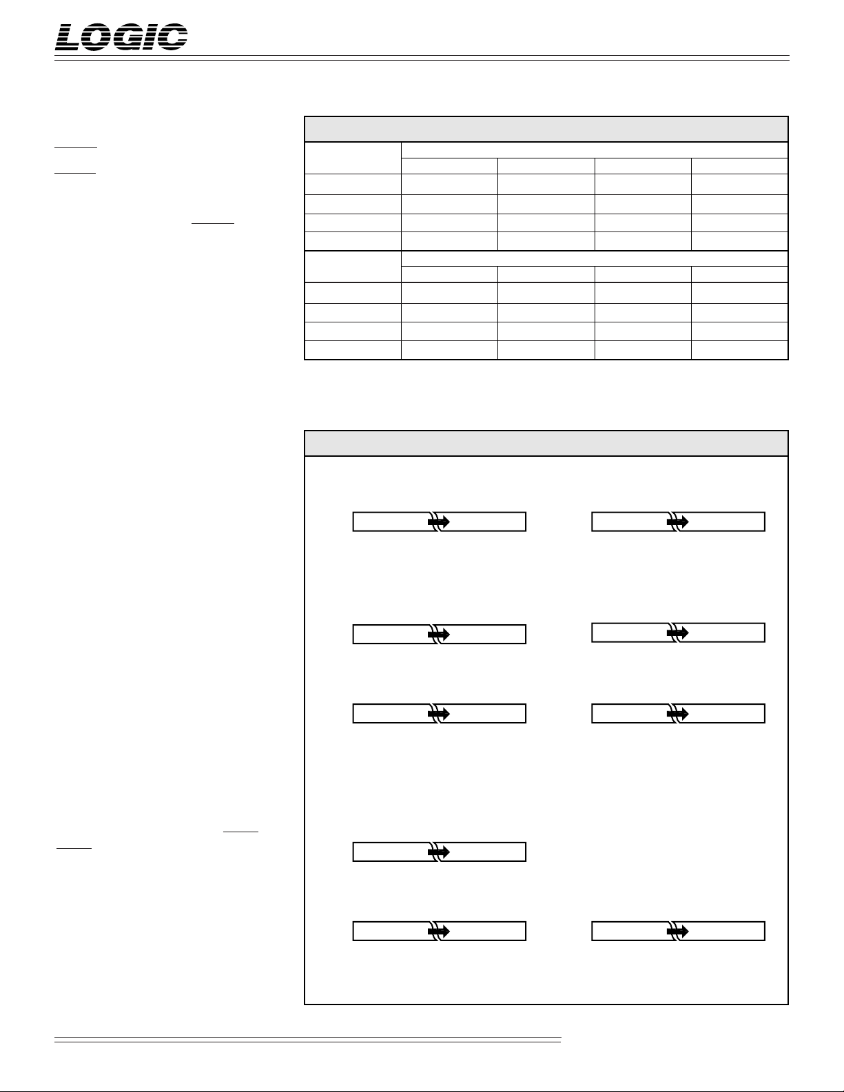
TABLE 1. INPUT/OUTPUT FORMATS
Input Input Format*
Channel 4:4:4:4 4:2:2:4 4:2:2:4 4:2:2:4
A12-0 R Y Y Y/Cb/Cr
B12-0 G Cb Cb/Cr N/A
C12-0 B Cr N/A N/A
D12-0 Key Key Key Key
Output Output Format*
Channel 4:4:4:4 4:2:2:4 4:2:2:4 4:2:2:4
W12-0 R Y Y Y/Cb/Cr
X12-0 G Cb Cb/Cr N/A
Y12-0 B Cr N/A N/A
Z12-0 Key Key Key Key
* Not all input/output combinations are valid. If single channel interleaved video
is used on either the input or output, the core clock will be running at CLK/2.
Thus the maximum input, output, and core data rate must be considered.
FIGURE 3. INPUT AND OUTPUT FORMATS
INPUT BIAS ADDER/OUTPUT BIAS ADDER
Input Data Output Data
12 11 10 2 1 0
12
–2
(Sign)
2112
10
22212
0
12 11 10 2 1 0
12
–2
(Sign)
2112
10
22212
0
If use of the Matrix Multiplier/Key Scaler is
desired, at least one Matrix Multiplier/Key
Scaler RSL Register Set and coefficient
address must be loaded and selected for
each channel. If use of the Input Bias Adder
is desired, at least one Input Bias Adder
Register must be loaded and selected before
use. If use of the Output Bias Adder is
desired, at least one Output Bias Adder
Register must be loaded and selected before
use. If use of the Look-Up Table is desired,
the Look-Up Table must be loaded before
use.
When using a single channel input or
output with interleaved video, SYNC and
RESET should be used for proper initialization as shown in Figure 5. If 12 bits or less
input data is desired, the input data should
be shifted so the MSBs are aligned.
Input Demultiplexer
The input demultiplexer section acts as a
buffer between the user’s datapath and the
MATRIX MULTIPLIER/KEY SCALER
Input Data
12 11 10 2 1 0
12
–2
(Sign)
2112
10
22212
0
Coefficient Data
12 11 10 2 1 0
–2
(Sign)
0
2–12
–2
–102–112–12
2
*Matrix Multiplier Output *Key Scaler Output
F19 F18 F17 F2 F1 F0
15
–2
(Sign)
*Format of Matrix Multiplier/Key Scaler ouput feeding the RSL Circuitry. F19-F0 corresponds to 20 MSBs of which a
13-bit window can be selected from F
2142
13
2–22–32
–4
19-F4 .
F19 F18 F17 F2 F1 F0
13
–2
(Sign)
2122
11
2–42–52
HALF-BAND FILTER
Input Data
12 11 10 2 1 0
12
–2
(Sign)
2112
10
22212
0
**Filter Output (Non-Interpolate) **Filter Output (Interpolate)
F19 F18 F17 F2 F1 F0
12
–2
(Sign)
*Format of Half-Band Filter ouput feeding the RSL Circuitry. F19-F0 corresponds to 20 MSBs of which a
13-bit window can be selected from F19-F4 (see Table 3).
2112
10
2–52–62
–7
F19 F18 F17 F2 F1 F0
13
–2
(Sign)
2122
11
2–42–52
–6
–6
Video Imaging Products
5
03/13/2001–LDS.3370-F
DEVICES INCORPORATED
LF3370
High-Definition Video Format Converter
LF3370’s core. Data may be presented on
input ports A12-0, B12-0, and C12-0 as three
channels of non-interleaved input data, one
channel non-interleaved and one channel
interleaved input data, or one channel of
interleaved data (see Table 1 for various
video input schemes). D12-0 is the Key
channel input port; the Key channel is
simply passed through the input
demultiplexer with a latency that matches
the other three channels.
If video data is non-interleaved and
presented to input ports A12-0, B12-0, and
C12-0, no demultiplexing is performed.
The three channels are passed unmodified
into the LF3370 core with a delay of 3 CLK
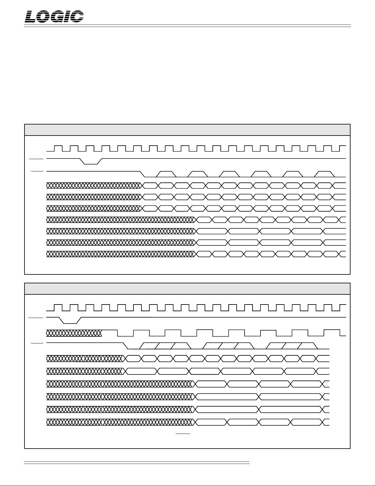
FIGURE 4. INPUT PROCESSING 4:2:2:4 (INTERLEAVED CHROMA ON CHANNEL B)
2
CLK
RESET
SYNC
A
12-0
12-0
B
D
12-0
A'
12-0**
B'
12-0**
1
3
41214
Y
CB
K
6
5
Y
1
0
CR0CB2CR
0
K
1
0
7
Y
2
Y
K
2
K
911
8
3
Y
4
2
CB
4
3
K
4
Y'
0
Y'
1
CB'
0
CR
cycles. For this operation, bits 0 and 1
must both be set to 1 in Configuration
Register 0 (see Table 5).
If video data is on two channels (see Figure
4), one channel of non-interleaved video
and one channel of interleaved video, it is
assumed that non-interleaved video is
presented to input port A12-0 (i.e., Luma)
10
Y
Y
Y
K
6
5
CR6CB
CB
6
4
K
K
6
5
Y'
Y'
3
2
CB'
2
13
7
Y
8
Y
8
CR
7
K
8
K
Y'
4
Y'
5
CB'
4
15
CB
CB'
Y
Y
10
CR
10
K
K
10
Y'
7
6
9
8
9
Y'
6
17
16
Y
12
11
CB
12
10
K
12
11
Y'
8
CB'
6
C'
D'
12-0**
12-0**
Demultiplexed Input Data (Output of Demux Section)
*
CR'
0
K'
0
K'
1
CR'
2
K'
K'
2
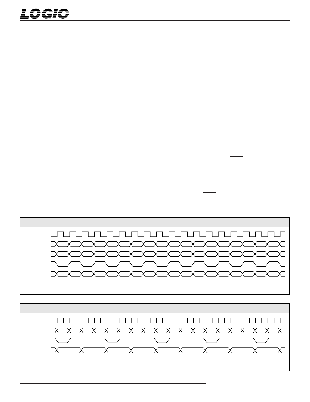
FIGURE 5. INPUT PROCESSING 4:2:2:4 (INTERLEAVED LUMA/CHROMA ON CHANNEL A)
41214
2
1
3
5
CLK
RESET
CLK/2*
SYNC
CB
12-0
A
12-0
D
A’
12-0**
B’
12-0**
C’
12-0**
0
K
0
6
7
Y0CR0Y
K
1
8
1
CB
10
911
2
Y
2
K
2
Y’
0
CB’
CR’
CR
2
0
0
K
3
Y’
Y3CB
1
CR'
17
6
K'
8
6
CR'
4
3
K'
4
K'
13
4
Y
4
K
4
Y’
2
5
CR
CB’
CR’
CR'
K'
6
15
Y
5
4
K
5
Y’
3
1
1
6
K'
7
16 18
CB
D’
12-0**
K’
K’
0
*
Core Clock (Internally Generated and Synchronized to CLK by RESET) Used Only When Single Channel Interleaved Input or Output Video is Used.
**
Demultiplexed Input Data (Output of Demux Section)
K’
1
2
K’
3
Video Imaging Products
6
03/13/2001–LDS.3370-F
DEVICES INCORPORATED
LF3370
High-Definition Video Format Converter
and interleaved video is presented to input
port B12-0 (i.e., Chroma). The input
demultiplexer, in this case, separates video
data on B12-0 and outputs two channels of
separated video into the LF3370 core with
a delay of 4 CLK cycles. For this operation,
bit 0 must be set to 0 and bit 1 must be set to
1 in Configuration Register 0 (see Table 5).
If 4:2:2 video data is on one channel
interleaved (see Figure 5), it is assumed
that interleaved video is presented to input
port A12-0. The input demultiplexer, in
this case, separates video data on A12-0
and outputs three channels of separated
video into the LF3370 core with a delay of
5 CLK cycles. In this case, the core will
run at half of the CLK rate and valid data
will be output at at half of the CLK rate.
For this operation, bit 0 must be set to 1
and bit 1 must be set to 0 in Configuration
Register 0 (see Table 5).
All input demultiplexing operations are
controlled by the latched HIGH to LOW
transitions of SYNC which synchronizes
the LF3370 core to the multiplexed input
data (see SYNC discussion). It is impor-
tant that unused input ports be set either
HIGH or LOW.
Output Multiplexer
The output multiplexer section can be
configured in various ways to accommodate the video system. Bits 2 and 3 of
Configuration Register 0 determines the
number of output channels that the
LF3370 will drive. Z12-0 is the Key
channel output port; the Key channel
simply gets passed through the output
multiplexer with a latency that matches
the other three channels.
If three separate output channels of noninterleaved video are desired, no multiplexing is performed. The three channels
are passed through the output multiplexer unmodified on the output ports
W12-0, X12-0, and Y12-0 with a delay of 2
CLK cycles. For this operation, bits 2 and
3 must both be set to 1 in Configuration
Register 0 (see Table 5).
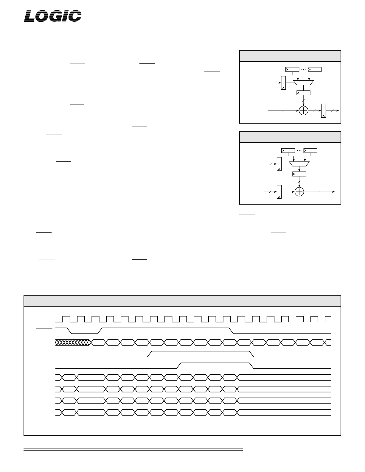
If one channel of non-interleaved video
(i.e., Luma) and one channel of inter-
leaved video (i.e., Chroma) is desired (see
Figure 6), non-interleaved video will be
driven to the output port W12-0 and
interleaved video will be driven to the
output port X12-0 with a delay of 2 CLK
cycles. For this operation, bit 2 must be set
to 0 and bit 3 must be set to 1 in Configuration Register 0 (see Table 5).
If 4:2:2 interleaved video on one port is
desired (see Figure 7), interleaved video
will be driven to the output port W12-0
with a delay of 4 CLK cycles. For this
operation, bit 2 must be set to 1 and bit 3
must be set to 0 in Configuration Register 0
(see Table 5).
All output multiplexing operations are
initiated by the latched HIGH to LOW
transitions of SYNC which synchronizes
the multiplexed output data to the LF3370
core (see SYNC discussion).
SYNC
SYNC control signal is required to
properly synchronize the input
demultiplexer, output multiplexer, and
FIGURE 6. OUTPUTTING 4:2:2:4 (INTERLEAVED CHROMA ON CHANNEL X)
CLK
Y1Y
2
Y
W
Y
0 (Output SYNC)*
12-0
X
12-0
Z
12-0
Y
0
CR0CB2CR
CB
0
K1K
K
0
There will be a HIGH to LOW transition on every Cb sample
*
3
Y
4
2
CB
2
K
3
K
4
Y
5
4
CR
4
K
5
Y
CB
K
6
6
6
Y
7
CR6CB
K
7
Y
8
Y
9
Y
10
8
CR
8
CB
10
K
8
K
9
K
10
FIGURE 7. OUTPUTTING 4:2:2:4 (INTERLEAVED LUMA/CHROMA ON CHANNEL W)
CLK
W
Y
0 (Output SYNC)*
12-0
Z
12-0
*
There will be a HIGH to LOW transition on every Cb sample
CB
0
K
Y0CR0Y
0
1
CB
2
Y
2
K
1
K
2
CR
2
Y3CB
K
3
4
Y
4
CR
4
K
K
4
5
CR
Y
Y
K
12
11
10
11
Y
5
CB
K
CB
Y
13
Y
14
12
CR
12
CB
14
12
K
13
K
14
6
Y
6
CR
6
K
K
6
7
CR
Y
16
Y
Y
15
CB
14
K
15
CR
Y
7
17
16
CR
16
K
16
K
17
8
Y
8
K
8
Video Imaging Products
7
03/13/2001–LDS.3370-F
DEVICES INCORPORATED
LF3370
High-Definition Video Format Converter
halfband filters to the data flowing
through the LF3370. A latched HIGH to
LOW transition on SYNC control signal is
needed to initialize the device to mark the
beginning of valid data.
In addition, if 4:2:2 interleaved video data
is desired for input or output, a HIGH to
LOW transition on SYNC must be
registered by a simultaneous rising edge of
CLK and CLK/2. CLK/2 is an internal
clock that must be synchronized to CLK
by use of RESET only if the core is running
at half the rate of CLK (see RESET
discussio n and Figures 4 & 5).
Furthermore, SYNC is used to identify one
interleaved data set from another. For
example, in the case of interleaved
Chroma, Cb and Cr samples must be
properly demultiplexed and synchronized for processing.
To differentiate a Cb sample from Cr, there
needs to be a HIGH to LOW transition on
SYNC on the first Cb sample (see Figure 4
& 5); SYNC can also be toggled on every
Cb sample for re-synchronization.
In the case that Cb is the first valid data
word, SYNC may be used only once in
device initialization and kept low until re-
synchronization is desired. Therefore,
when there is a HIGH to LOW transition
on SYNC, the following is assumed: Cb
will occur on the first LOW on SYNC that
is latched, Cb will occur every two clock
cycles if interleaved Chroma is presented
to the input port B12-0, Cb will occur every
4 clock cycles if single channel 4:2:2
interleaved video is presented to the input
port A12-0.
SYNC control signal is also used to
synchronize the interpolation/decimation
output data from the Half-Band Filter to
the Output Multiplexer. This synchronization is done automatically.
RESET
RESET should be used when initializing
the device for proper operation. It is used
to synchronize the LF3370 core clock to
the master clock. In the case that single
channel 4:2:2 interleaved video data is
desired either on the input or output, thus
using only one input or one output port
(not including Key data), the internal
clock rate will be half (CLK/2) of the
master clock rate (CLK). In this case,
RESET is needed to synchronize the rising
edge of CLK/2 to a known rising edge of
CLK (see Figure 4). For example, after
configuring the LF3370 and before
FIGURE 8. INPUT BIAS
R0R3
INBIAS
From Input Demux
2
1-0
13
13
13
13
FIGURE 9. OUTPUT BIAS
R0R3
OUTBIAS
From Core
streaming valid data through the part, a
RESET event should be used to align the
clock edges (see Figure 4 & 5).
Furthermore, RESET will clear HF0 and
HF1. A LOW state detected on RESET on a
rising edge of clock will clear flags HF0
and HF1 on the following rising edge of
clock. Please note HBLANK should be
2
1-0
13
13
13
FIGURE 10. HBLANK AND COUNTER
CLK
HBLANK
20-bit
COUNTER
HF
HF
A'
12-0*
B'
12-0*
C'
12-0*
D'
12-0*
2
1
0
0
1
D
N
HBLANK Word A
D
N
HBLANK Word B
D
N
HBLANK Word C
D
N
HBLANK Word D
Data values at output of Input LUT section
*
In this example, HF0 Count Value is set to 3 and HF1 Count Value is set to 5
41214
3
123
D
N+3DN+4DN+5
D
N+3DN+4DN+5
D
N+3DN+4DN+5
D
N+3DN+4DN+5
6
5
4
D
N+6
D
N+6
D
N+6
D
N+6
7
5
D
N+7
D
N+7
D
N+7
D
N+7
8
6
D
N+8
D
N+8
D
N+8
D
N+8
10
911
78
D
N+9DN+10
D
N+9DN+10
D
N+9DN+10
D
N+9DN+10
9
D
N+11
D
N+11
D
N+11
D
N+11
13
0
10
15
1
23
HBLANK Word A
HBLANK Word B
HBLANK Word C
HBLANK Word D
1716 18
4
5
Video Imaging Products
8
03/13/2001–LDS.3370-F
 Loading...