DEVICES INCORPORATED
LF2301
Image Resampling Sequencer
LF2301
DEVICES INCORPORATED
FEATURES DESCRIPTION
❑❑
❑ 40 MHz Clock Rate
❑❑
❑❑
❑ High-Speed Image Manipulation
❑❑
❑❑
❑ Maximum Image Size: 4096 x 4096
❑❑
Pixels
❑❑
❑ Supports Following Interpolation
❑❑
Algorithms:
• Nearest-Neighbor
• Bilinear Interpolation
• Cubic Convolution
❑❑
❑ Applications:
❑❑
• Video Special-Effects
• Image Recognition
• High-Speed Data Encoding/
Decoding
❑❑
❑ Replaces TRW/Raytheon/Fairchild
❑❑
TMC2301
❑❑
❑ 68-pin PLCC, J-Lead
❑❑
The LF2301 is a self-sequencing
address generator designed to filter
a two-dimensional image or remap
and resample it from one set of
Cartesian coordinates (x,y) into a
new set (u,v).
The LF2301 can resample digitized
images or perform such manipulations as rotation, panning, zooming,
and warping as well as compression
in real-time.
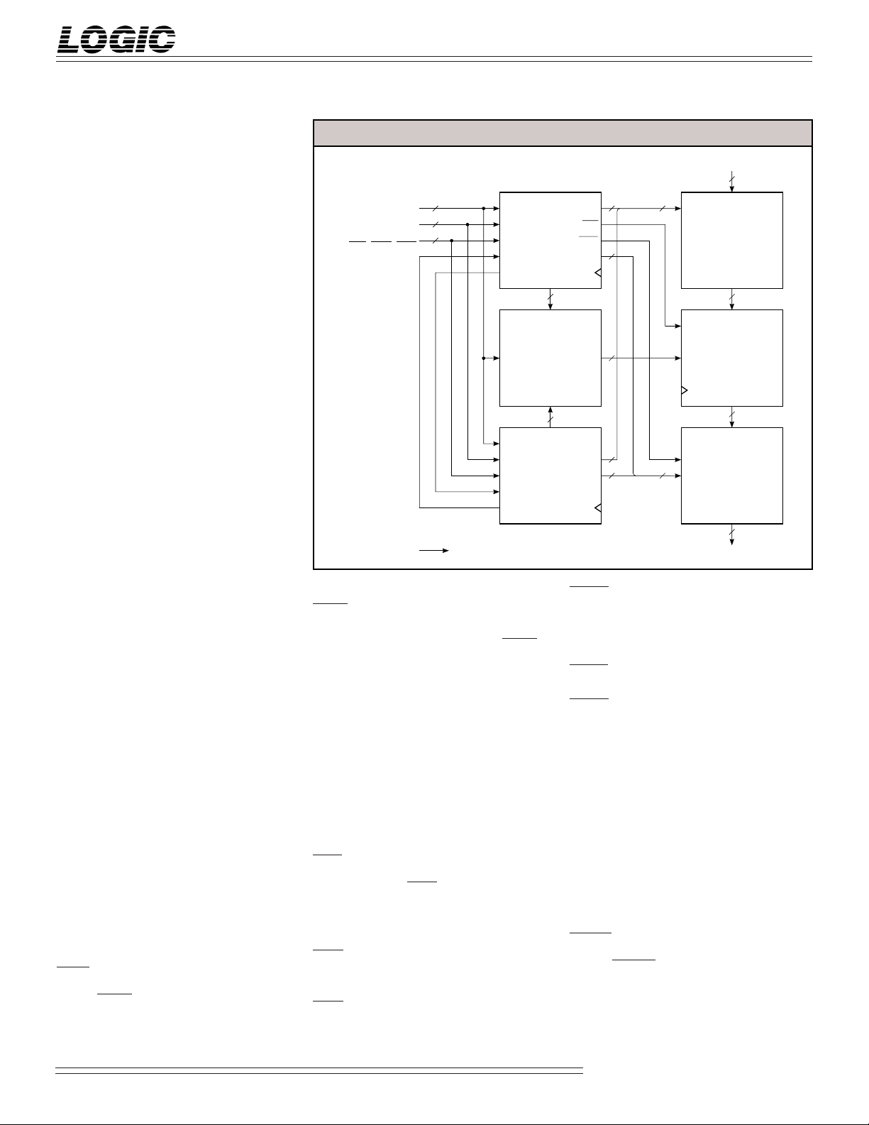
By using two LF2301s in a Image
Transformation System (ITS),
nearest-neighbor, bilinear interpolation, and cubic convolution algorithms, with kernel sizes up to 4 x 4
pixels, are all possible (see Figure 1).
This system can also implement
simple static filters with kernel sizes
up to 16 x 16 pixels.
Image Resampling Sequencer
DETAILS OF OPERATION
Most video applications use a pair
of LF2301s in tandem to construct
an ITS. One LF2301 is the row
coordinate generator (x to u) and the
other is the column generator (y to
v). External RAM is needed for
storage of the interpolation coefficient lookup table, as well as for
buffers of the source and destination
images. An external MultiplierAccumulator is required when
performing interpolation or implementing static filters.
The ITS is capable of performing the
general second-order coordinate
transformation of the form:
x(u,v) = Au2+Bu+Cuv+Dv2+Ev+F
y(u,v) = Gu2+Hu+Kuv+Lv2+Mv+N
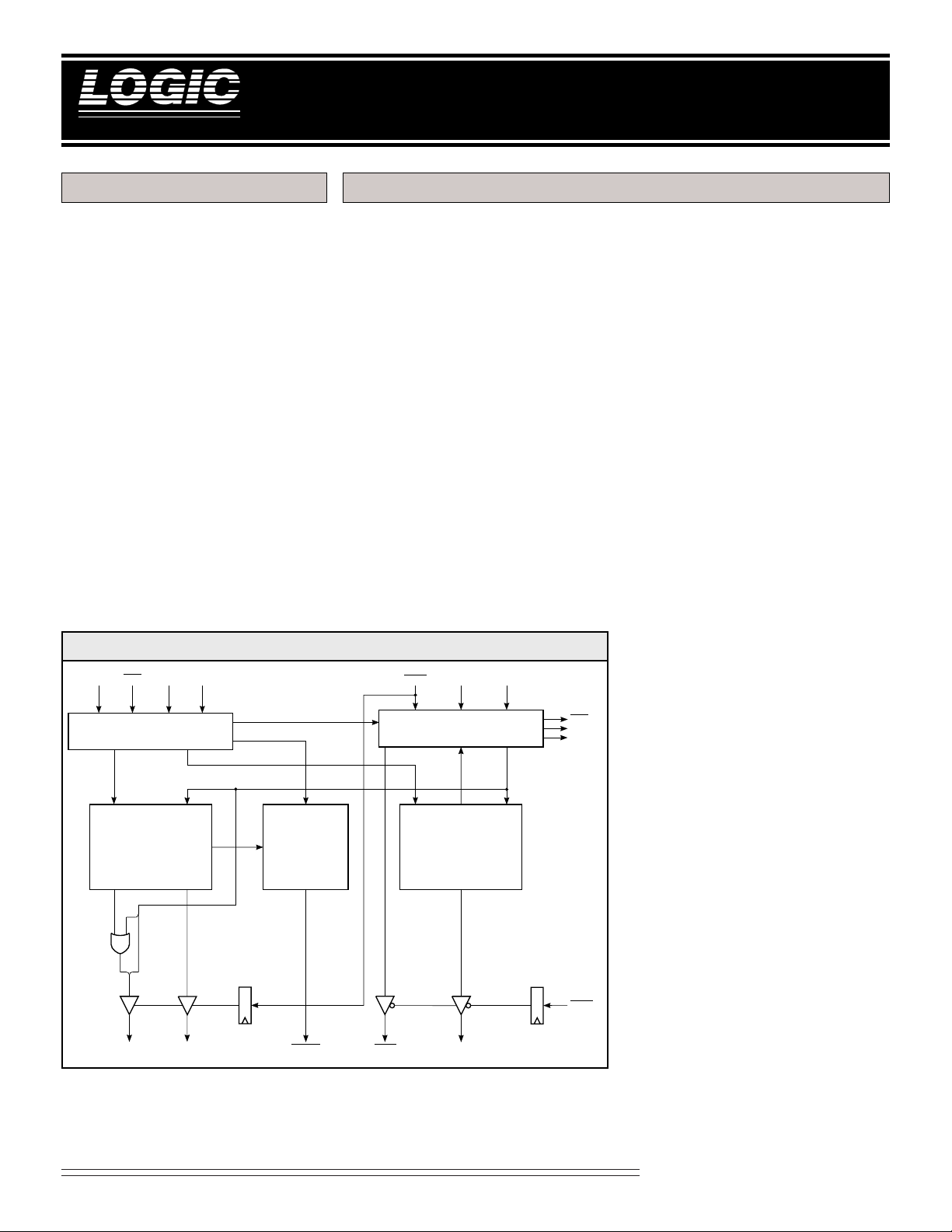
LF2301 BLOCK DIAGRAM
WENLDR B
3-0P11-0
PARAMETER
STORAGE
SOURCE
ADDRESS
GENERATOR
INTEGERFRACTION
11-0CA7-0
X
INPUT IMAGE
BOUNDARY
COMPARATOR
CZERO
UWRI
INTER INITNOOP
CONTROL
WALK COUNT
TARGET
ADDRESS
GENERATOR
U
11-0
ACC
DONE
END
OETA
where parameters A through N of
the transform are user-defined.
The system steps sequentially
through each pixel in the “target”
image lying within a user-defined
rectangle. For each “target” pixel
at (u,v), the LF2301 points to a
corresponding “source” pixel at
(x,y).
2-1
Video Imaging Products
08/16/2000–LDS.2301-H
DEVICES INCORPORATED
LF2301
Image Resampling Sequencer
SIGNAL DEFINITIONS
Power
Vcc and GND
+5V power supply. All pins must be
connected.
Clock
CLK — Master Clock
The rising edge of CLK strobes all
enabled registers.
Inputs
P11-0 — Parameter Register Data Input
P11-0 is the 12-bit Parameter Register
Data input port. P11-0 is latched on
the rising edge of CLK.
B3-0 — Parameter Register Address Input
B3-0 is the 4-bit Parameter Register
Address input port. B3-0 is latched on
the rising edge of CLK.
Outputs
FIGURE 1. IMAGE TRANSFORMATION SYSTEM (ITS)
P
11-0
B
INIT, LDR,
WEN, NOOP, OETA
CLK
12
4
3-0
5
INTER
END
INTERPOLATION
COEFFICIENT
INTER
END
LF2301
Row
Address
Generator
(X)
7-0
CA
8
RAM
8
7-0
CA
LF2301
Column
Address
Generator
(Y)
X
ACC
UWRI
U
Y
V
11-0
11-0
11-0
11-0
12 24
12
12
12
12
IMAGE DATA IN
12
SOURCE
IMAGE
RAM
12
ACC
Y
24
X
LMA1009/2009
12 x 12 bit
Multiplier-
Accumulator
X,Y,P
D
OUT
12
DESTINATION
IMAGE
RAM
12
IMAGE DATA OUT
X11-0 — Source Address Output
X11-0 is the 12-bit registered Source
Address output port.
CA7-0 — Coefficient Address Output
CA7-0 is the 8-bit registered Coefficient Address output port.
U11-0 — Target Address Output
U11-0 is the 12-bit registered Target
Address output port.
Controls
INIT — Initialize
When INIT is HIGH for a minimum of
two clock cycles, the control logic is
cleared and initialized for the start of a
new image transformation. When
INIT goes LOW, normal operation
begins after two clock cycles. INIT is
latched on the rising edge of CLK.
WEN — Write Enable
When WEN is LOW, data latched into
the device on P11-0 is loaded into the
preload register addressed by the data
latched into the device on B3-0. When
WEN is HIGH, data cannot be loaded
into the preload registers and their
contents will not be changed. WEN is
latched on the rising edge of CLK.
LDR — Load Data Register
When LDR is HIGH, data in all
preload registers is latched into the
Transformation Parameter Registers.
When LDR is LOW, data cannot be
loaded into the Transformation
Parameter Registers and their contents
will not be changed. LDR is latched
on the rising edge of CLK.
ACC — Accumulate
The registered ACC output initializes
the accumulation register of the
external multiplier-accumulator. At
the start of each interpolation “walk,”
ACC goes LOW for one cycle effectively clearing the storage register by
loading in only the new first product.
ACC from either the row or column
LF2301 may be used.
UWRI — Target Memory Write Enable
The Target Memory Write Enable goes
LOW for one clock cycle after the end
of each interpolation “walk.” When
OETA is HIGH, this registered output
is forced to the high-impedance state.
UWRI from either the row or column
LF2301 may be used.
INTER — Interconnect
When two LF2301s are used to form
an ITS, the END flag on each device
is connected to INTER on the other
device. The END flag from the row
device indicates an “end of line” to the
column device. The END flag from the
column device indicates a “bottom of
frame” to the row device, forcing a
reset of the address counter.
NOOP — No Operation
When NOOP is LOW, the clock is
overridden holding all address
generators in their current state. X11-0
and CA7-0 are forced to the high-
2-2
Video Imaging Products
08/16/2000–LDS.2301-H

DEVICES INCORPORATED
LF2301
Image Resampling Sequencer
impedance state. Users may then
access external memory. Normal
operation resumes on the next clock
cycle after NOOP goes HIGH. NOOP
is latched on the rising edge of CLK.
OETA — Target Memory Output Enable
When OETA is HIGH, UWRI and U11-0
are forced to the high-impedance
state. When OETA is LOW, UWRI
and U11-0 are enabled on the next
clock cycle. OETA is latched on the
rising edge of CLK.
Flags
CZERO — Coefficient Zero
If in a row device x<0,
XMIN≤x≤XMAX, or x≥4096, the
registered CZERO flag goes HIGH . If
0≤x<XMIN or XMAX<x<4096, CZERO
goes LOW. In an ITS, when the source
address falls outside a rectangle with
vertices (XMIN, YMIN), (XMAX,
YMIN), (XMIN, YMAX), and (XMAX,
YMAX), the logical AND of the
CZERO flags from the row and
column of the LF2301s will go LOW
representing an invalid address.
END — End of Row/Frame
When two LF2301s are used to form
an ITS, the END flag on each device
is connected to INTER on the other
device. The END flag from the row
device indicates an “end of line” to the
column device. The END flag from
the column device indicates a “bottom
of frame” to the row device, forcing a
reset of the address counter.
When Mode is set to “00” or “10”
END goes HIGH on the row device
for (K+1) x (K+1) clock cycles
starting[2 x (K+1) x (K+1)] + 1 clock
cycles before the last X address of a
row. END goes HIGH on the column
device for (K+1)3 x (UMAX-UMIN)
clock cycles starting at (K+1)3 x
(UMAX-UMIN) + 1 clock cycles before
the last X address of a frame.
When Mode is set to “01” or “11”
END goes HIGH on the row device
for K+1 clock cycles starting at (K+1) +
2 clock cycles before the last X address
of a row. END goes HIGH on the
column device for (K+1) x (K+1)
clock cycles starting at [(K+1) x (K+1)] +
1 clock cycles before the last X address
of a frame.
DONE — End of Transform
In a two LF2301 system, after the last
walk of the last row of an image, the
registered DONE flag goes HIGH
indicating the end of the transform.
DONE goes HIGH one clock cycle
before the last X address of a frame. If
AIN is HIGH, DONE will remain
HIGH for one clock cycle. If AIN is
LOW, DONE will remain HIGH until
a new transform begins.
Transformation Control Parameters
XMIN, XMAX, YMIN, YMAX
XMIN, XMAX, YMIN, YMAX define
the valid area in the source image
from which pixels may be read. The
CZERO flags will denote a valid
memory read whenever the LF2301s
generate an (x,y) address within this
boundary.
UMIN, UMAX, VMIN, VMAX
UMIN, UMAX, VMIN, VMAX define
the area in the destination image into
which pixels will be written.
(UMIN, VMIN) is the top left corner
and (UMAX + 1, VMAX) is the bottom
right corner. The following conditions
must be met: UMAX>UMIN and
VMAX>VMIN.
x0, y0
x0, y0 determine what the first pixel read
out of the source image will be at the
beginning of an image transformation.
x0, y0 will be the upper left corner of the
original image in non-inverting, nonreversing applications.
dx/du
dx/du is the displacement along the
x axis corresponding to a one-pixel
movement along the u axis.
2-3
dx/dv
dx/dv is the displacement along the
x axis corresponding to each one-pixel
movement along the v axis.
dy/du
dy/du is the displacement along the
y axis corresponding to each one-pixel
movement along the u axis.
dy/dv
dy/dv is the displacement along the
y axis corresponding to each one-pixel
movement along the v axis.
2
d2x/du
d2x/du2 determines the rate of change
of dx/du with each step along a line
in the output image.
2
d2x/dv
d2x/dv2 determines the rate of change
of dx/dv with each step down a
column in the output image.
2
d2y/du
d2y/du2 determines the rate of change
of dy/du with each step along a line
in the output image.
2
d2y/dv
d2y/dv2 determines the rate of change
of dy/dv with each step down a
column in the output image.
d2x/dudv
d2x/dudv determines the rate of
change of dx/du while moving
vertically through the output image.
d2x/dudv also determines the rate of
change of dx/dv while moving
horizontally through the output
image.
d2y/dudv
d2y/dudv determines the rate of
change of dy/dv while moving
horizontally through the output
image. d2y/dudv also determines the
rate of change of dy/du while
moving vertically through the output
image.
Video Imaging Products
08/16/2000–LDS.2301-H
DEVICES INCORPORATED
LF2301
Image Resampling Sequencer
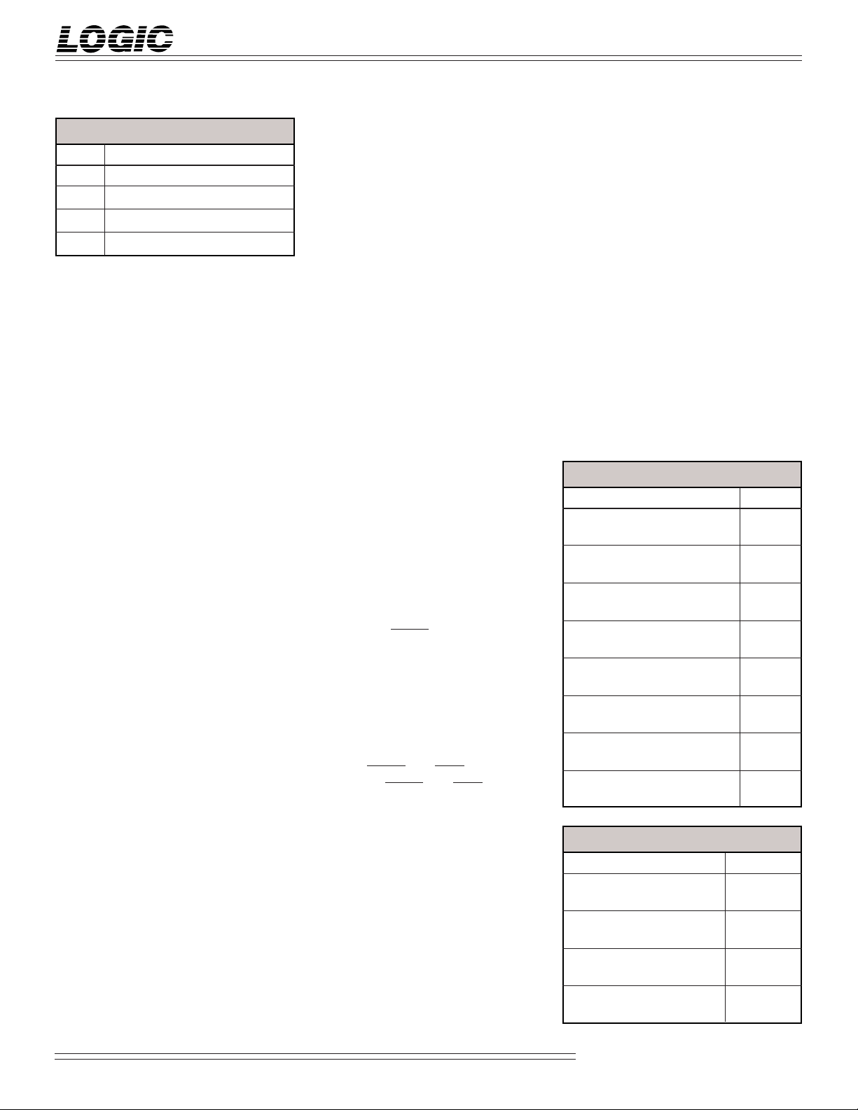
TABLE 1. MODE SELECTION
M1 M0 MODE
0 0 single-pass operation (CW)
0 1 pass 1 of two-pass operation
1 0 single-pass operation (CCW)
1 1 pass 2 of two-pass operation
R/C — Row/Column Select
When set to 0, the LF2301 functions as
a row device. When set to 1, the
LF2301 functions as a column device.
M1-0 — Mode
This 2-bit control word defines four
modes as follows (see table 1):
The 1st and 3rd modes are singlepass operations where the device
walks through a (K + 1) x (K + 1)
kernel for each output pixel. K is the
kernel size determined by K3-0 in
Parameter Register 7. In mode 00, the
spiral walk is in the clockwise direction. In mode 10, the spiral walk is in
the counter clockwise direction.
The 2nd and 4th modes are used
together to perform a two-pass
operation. The first pass (mode 01)
performs a (K+1) kernel in the
horizontal dimension. The second
pass (mode 11) performs a (K+1)
kernel in the vertical dimension.
The result of pass 1 is stored in the
destination image memory and is used
as the source image data for the second
pass. A system to switch source and
destination memory banks could be
designed, or utilization of a second
LF2301 pair in a pipelined architecture
could be used. In this case, the system
would require a third image buffer for
the final destination image.
K3-0 — Kernel
Kernel determines the length of the
spiral walk when performing image
transformations and the size of the
filter when implementing static filters
(see table 2). When performing image
transformations, the longest spiral walk
possible is 4 x 4 pixels (Kernel = 3). For
static filters, kernels of up to 16 x 16
pixels (Kernel = 15) are possible.
FOV — Field of View
FOV determines the distance between
pixels in a spiral walk. An FOV of 1
means each step in a spiral walk is one
pixel. An FOV of 2 means each step is
two pixels, and so on. FOV can be set
as high as 7 (see Table 3). It is important to note when FOV is 0, the x and
y addresses will not change during a
spiral walk. They will remain fixed at
the first pixel address of the spiral
walk.
ALR — Autoload
When set HIGH and upon INIT being
strobed, the LDR control is automatically
asserted which causes the data
currently stored in the Preload Registers
to be loaded into the Transformation
Parameter Registers.
AIN — Autoinit
A new transform automatically begins
if the AIN bit is HIGH when the end of
an image is reached. The DONE flag
will go HIGH for one clock cycle. If
AIN is LOW, UWRI and the DONE flag
remain HIGH until the user strobes the
INIT control to begin a new image
transformation.
PIPE — Pipe Control
In order to compensate for buffered
source image RAM, PIPE adjusts the
timing of UWRI and ACC. If the PIPE
bit is HIGH, UWRI and ACC will have
a one clock cycle delay added relative
to the generation of the target address.
TM — Test Mode
Calculations of the source image and
coefficient addresses are made by an
internal 28-bit accumulator. TM
allows access to the sign bit and the
seven bits below the four coefficient
address bits in the accumulator. When
TM is HIGH the sign bit and 11 bits
below the source image address are fed
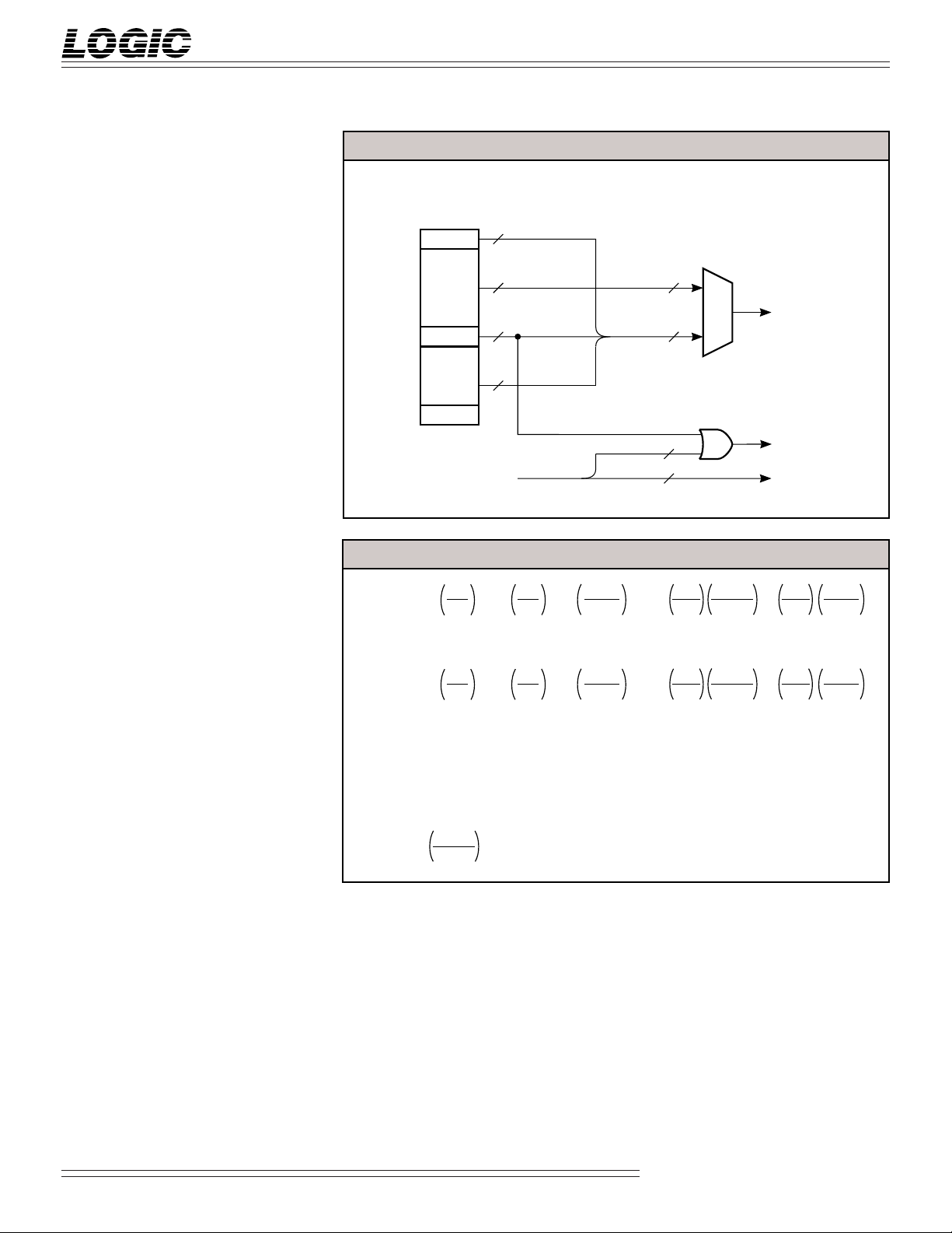
to X11-0 (see Figure 2). When TM is
LOW, the source image address is fed
to X11-0. Two clock cycles are required
to access both the MS and LS words of
the internal accumulator.
Functional Description
The LF2301 is an address generator
designed to be used in an image
transformation system (ITS). When
implementing an LF2301-based ITS,
second-order image transformations
can be performed like resampling,
rotation, warping, panning, and
rescaling, all at real-time video rates.
2D filtering operations, like pixel
convolutions, can also be performed.
In most applications two LF2301s are
used, one to generate the row addresses
and the other to generate the column
TABLE 2. KERNEL
K3 K2 K1 K0 Kernel
00 00 1 x 1
00 01 2 x 2
00 10 3 x 3
00 11 4 x 4
01 00 5 x 5
01 01 6 x 6
01 10 7 x 7
01 11 8 x 8
10 00 9 x 9
10 0110 x 10
10 1011 x 11
10 1112 x 12
11 0013 x 13
11 0114 x 14
11 1015 x 15
11 1116 x 16
TABLE 3. FIELD OF VIEW
F2 F1 F0 FOV
000 0
001 1
010 2
011 3
100 4
101 5
110 6
111 7
2-4
Video Imaging Products
08/16/2000–LDS.2301-H
DEVICES INCORPORATED
LF2301
Image Resampling Sequencer
addresses. An example of an ITS
implemented with two LF2301s is
shown in Figure 1. In this system the
following components are used: two
LF2301s, a multiplier-accumulator
(MAC), interpolation coefficient RAM,
and source/target image RAM.
Maximum image size is 4096 x 4096
pixels. Data word size is determined
by the word size of the external RAM.
A typical ITS performs image transformations as follows:
a. The LF2301s generate sequential
pixel addresses (left to right, top to
bottom) which fill the rectangle in the
target image RAM defined by
(UMIN,VMIN) and (UMAX +1, VMAX).
It is important to note that the U value
of the last pixel address on each line of
the target RAM is UMAX + 1.
b. The LF2301s calculate the address
of the corresponding pixel in the
source image RAM for each target
pixel address generated.
c. If interpolation is needed, the
external MAC sums the products of
the source pixels and the interpolation coefficients. Control signals for
the MAC and address signals for the
interpolation coefficient RAM are
provided by the LF2301s.
FIGURE 2. TEST MODE DATA ROUTING
28-BIT INTERNAL
ACCUMULATOR
SIGN
WALK COUNTER
1
12
4
7
12
12
4
4
FIGURE 3. ADDRESS TRANSFORMATION EQUATIONS
+
+
+=x
0
FOV CAX(w)·
+=y
0
FOV CAY(w)·
dx
du
dy
du
m+ n+ mn+ +x
m+ n+ mn+ +y
dx
dv
+
FOV m CAX(ker)·
dy
dv
FOV m CAY(ker)·+·
·
2
d x
dudv
2
d y
dudv
2
d x
du
2
d y
du
2
2
m – m
m – m
X11-0/T11-0
CA7-4
CA3-0
2
2
2
2
2
d x
dv
2
d y
dv
2
n – n
2
2
2
n – n
2
2
d. The new pixel value is written into
the target image RAM.
The LF2301s generate source pixel
addresses according to the following
general second order equations:
x = Au2 + Bu + Cuv + Dv2 + Ev + F
y = Gu2 + Hu + Kuv + Lv2 + Mv + N
where (x,y) and (u,v) are the source
and target coordinates respectively.
A through N are user-defined parameters. The actual second order equations used are shown in Figure 3.
UMIN
VMIN
NOTE:
m=u
+
n=v
+
2
m – m
2
APPROXIMATES THEEXPONENTIAL CHARACTERISTIC OF
Video Imaging Products
2-5
2
m
.
08/16/2000–LDS.2301-H
DEVICES INCORPORATED
LF2301
Image Resampling Sequencer
Transformation Parameter Register
Loading
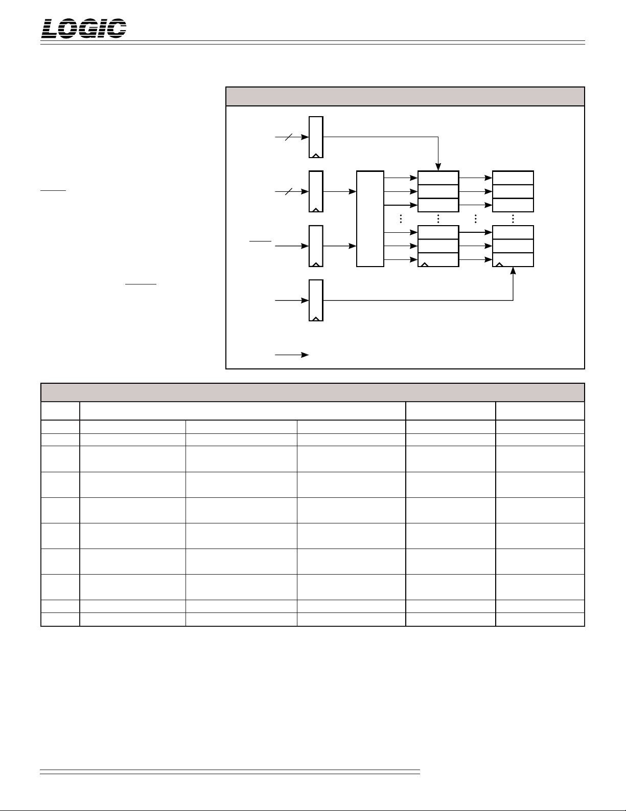
The LF2301 allows Transformation
Parameters to be updated on-the-fly.
The loading of these registers is
double-buffered (see Figure 4). Any
or all of the first level registers can
be loaded using P11-0, B3-0, and
WEN without affecting the parameters currently in use.
LDR simultaneously updates all
Transformation Parameter Registers.
If Autoload (ALR) is active, these
registers will be updated automatically at the beginning of each new
image. Note that NOOP does not
affect the loading of the Transformation Parameter Registers.
FIGURE 4. LDR CONTROL FOR PARAMETER UPDATE
P11-0
3-0
B
WEN
LDR
CLK
12
4
C15
C14
C13
DECODE
C2
C1
C0
PRELOAD
REGISTERS
TRANSFORMATION
PARAMETER
REGISTERS
TABLE 4. PARAMETER REGISTER FORMATS (ROW OR COLUMN MODE)
ADDR MSB FORMAT LSB ROW COLUMN
10
9
8
7
6
5
4
3
2
1
0000 2112
0001 2112
0010 262
2
2
2
10
9
2
5
2
8
2
4
3
2
2
7
2
2
6
2
2
1
2
0011 ALR AIN PIPE R/C M1 M0 –2
–2
–3
–4
–5
0100 2–12
2
2
2
0101 TM F2 F1 F0 –2
–2
–3
0110 2–12
2
–4
2
2
0111 K 3 K2 K1 K0 –272
1000 2–92
1001 –232
1010 2–92
1011 –232
1100 2–92
1101 –232
1110 2112
1111 2112
–102–112–122–132–142–152–162–172–182–192–20
2
1
2
–102–112–122–132–142–152–162–172–182–192–20
2
2
–102–112–122–132–142–152–162–172–182–192–20
2
2
10
2
10
2
0
2
2
1
0
2
2
1
0
2
9
9
2
8
2
2
8
2
2
–6
2
7
6
2
–5
–6
2
6
–1
–2
2
–1
–2
2
–1
–2
2
7
6
2
7
6
2
2
2
2
2
5
4
2
2
0
2
2
12
2
–7
2
2
5
2
2
–7
2
2
5
2
2
–3
2
2
–3
2
2
–3
2
2
5
2
2
5
2
2
3
2
–1
–2
2
11
10
2
–8
–9
2
4
3
2
–8
–9
2
4
3
2
–4
–5
2
–4
–5
2
–4
–5
2
4
3
2
4
3
2
2
2
2
2
–3
2
2
9
2
2
–102–112–12
2
2
2
2
–102–112–12
2
2
2
2
–6
2
2
–6
2
2
–6
2
2
2
2
2
2
2
2
0
2
1
0
2
–4
–5
2
8
7
2
XMIN YMIN
XMAX YMAX
x0 (LS) y0 (LS)
Controls, x0 (MS) Controls, y0 (LS)
dx/du (LS) dy/du (LS)
1
20Controls, dx/du (MS) Controls, dy/du (MS)
dx/dv (LS) dy/dv (LS)
1
0
2
Kernel, dx/dv (MS) Kernel, dy/dv (MS)
d2x/dudv (LS) d2y/dudv (LS)
–7
–8
2
d2x/dudv (MS) d2y/dudv (MS)
d2x/du2 (LS) d2y/du2 (LS)
–7
–8
2
d2x/du2 (MS) d2y/du2 (MS)
d2x/dv2 (LS) d2y/dv2 (LS)
–7
–8
2
1
0
2
1
0
2
d2x/dv2 (MS) d2y/dv2 (MS)
UMIN VMIN
UMAX VMAX
2-6
Video Imaging Products
08/16/2000–LDS.2301-H
 Loading...