

DEVICES INCORPORATED
LF2250
12 x 10-bit Matrix Multiplier
LF2250
DEVICES INCORPORATED
FEATURES DESCRIPTION
❑❑
❑ 50 MHz Data and Computation
❑❑
Rate
❑❑
❑ Nine Multiplier Array with 12-bit
❑❑
Data and 10-bit Coefficient Inputs
❑❑
❑ Separate 16-bit Cascade Input and
❑❑
Output Ports
❑❑
❑ On-board Coefficient Storage
❑❑
❑❑
❑ Four User-Selectable Filtering and
❑❑
Transformation Functions:
• 3 x 3 Matrix Multiplier
• Cascadable 9-Tap FIR Filter
• Cascadable 3 x 3 Convolver
• Cascadable 4 x 2 Convolver
❑❑
❑ Replaces TRW/Raytheon/
❑❑
Fairchild TMC2250
❑❑
❑ 120-pin PQFP
❑❑
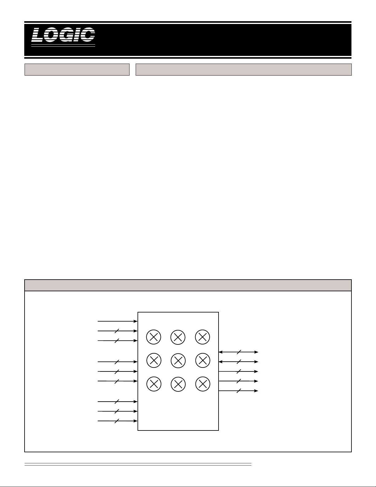
The LF2250 is a high-speed matrix
multiplier consisting of an array of
nine 12 x 10-bit multipliers. Internal
summing adders are also included to
provide the configurations needed to
implement matrix multiplications,
cascadable FIR filters, and pixel
convolvers.
The 3 x 3 matrix multiplier (triple dot
product) configuration of the LF2250
allows users to easily perform threedimensional perspective translations or
video format conversions at real-time
video rates. By using the LF2250 in
this configuration, conversions can be
made from the RGB (color component)
format to the YIQ (quadrature encoded
chrominance) or YUV (color difference) formats and vice versa (YIQ or
YUV to RGB).
In addition to color space conversions,
the LF2250 offers a range of selectable
configurations designed for filtering
applications. When configured as a
9-tap FIR filter, the LF2250 automatically
12 x 10-bit Matrix Multiplier
selects the necessary internal bus
structure and inserts the appropriate
data path delay elements. In addition,
a 16-bit cascade input port allows for
the creation of larger filters without a
reduction in throughput.
Real-time video image filtering using
the convolver modes of the LF2250 can
provide edge detection, texture
enhancement, and detail smoothing.
Both pixel convolver configurations,
3 x 3 and 4 x 2, deliver high-speed data
manipulation in a single chip solution.
By using the 16-bit cascade input port
to cascade two devices, cubic convolutions (4 x 4-pixel) can be easily accommodated with no decrease in throughput rates.
All inputs and outputs, as well as all
control lines, are registered on the
rising edge of clock. The LF2250
operates at clock rates up to 50 MHz
over the full commercial temperature
and supply voltage ranges.
LF2250 BLOCK DIAGRAM
CLK
1-0
MODE
CWE
1-0
A
DATA
INPUTS
COEFFICIENT
INPUTS
{
{
B
C
KA
KB
KC
11-0
11-0
11-0
9-0
9-0
9-0
2
2
12
12
12
12
10
10
10
9-MULTIPLIER
ARRAY
4
4
4
12
DATA
{
OUTPUTS
X
11-0
CASIN
Y
11-8
CASIN
Y
7-4
Y
3-0
CASOUT
Z
11-0
CASOUT
CASCADE
{
PORTS
15-4
XC
3-0
YC
Y
3-0
YC
15-4
ZC
PIN
{
NAME
11-0
11-8
7-4
3-0
11-0
Video Imaging Products
1
08/16/2000–LDS.2250-L

DEVICES INCORPORATED
LF2250
12 x 10-bit Matrix Multiplier
TABLE 1. MODE SELECTION
MODE1-0 OPERATING MODE
00 3 x 3 Matrix Multiplier
01 9-Tap FIR Filter
10 3 x 3 Convolver
11 4 x 2 Convolver
OPERATING MODES
The LF2250 can realize four different
user-selectable digital filtering architectures as determined by the state of the
mode (MODE1-0) inputs. Upon
selection of the desired function, the
LF2250 automatically chooses the
appropriate internal data paths and
input/output bus structure. Table 1
details the modes of operation.
DATA FORMATTING
The coefficient input ports (KA, KB,
KC) are 10-bit fractional two’s complement format regardless of the operating
mode. The data input ports (A, B, C)
are 12-bit integer two’s complement
format regardless of the operating
mode.
In the matrix multiplier mode (Mode
00), the data output ports (X, Y, Z) are
12-bit integer two’s complement
format. In the FIR filter and convolver
modes (Modes 01, 10, 11), the X, Y, and
Z ports are configured as the cascade-in
(CASIN15-0) and cascade-out
(CASOUT15-0) ports. These ports
assume 16-bit (12-bit integer, 4-bit
fractional) two’s complement data on
both the inputs and outputs. Table 2
shows the data port formatting for
each of the four operating modes.
BIT WEIGHTING
The internal sum of products of the
LF2250 can grow to 23 bits. However,
in order to keep the output format of
the matrix multiply mode (Mode 00)
identical to the input format, the X, Y,
and Z outputs are truncated to 12-bit
integer words. In the filter modes
(Modes 01, 10, 11), the cascade output
is always half-LSB rounded to 16 bits
(12 integer bits and 4 fractional bits).
The user may half-LSB round the
output to any size less than 16 bits by
simply forcing a “1” into the bit
position of the cascade input immediately below the desired LSB. For
example, if half-LSB rounding to 12
bits is desired, then a “1” must be
forced into the CASIN3 bit position
(CASOUT4 would then be the LSB).
In all four modes, the user may adjust
the bit weighting, by applying an
identical scaling correction factor to
both the input and output data
streams. If the coefficients are rescaled, then the relative weightings of
the cascade-in and cascade-out ports
will differ accordingly. Figure 1
illustrates the input and output bit
weightings for all four modes.
DATA OVERFLOW
Because the LF2250’s matched input
and output data formats accommodate
unity gain (0 dB), input conditions that
could lead to numeric overflow may
exist. To ensure that no overflow
conditions occur, the user must be
aware of the maximum input data and
coefficient word sizes allowable for
each specific algorithm being performed.
SIGNAL DEFINITIONS
Power
VCC and GND
+5 V power supply. All pins must be
connected.
Clock
CLK — Master Clock
The rising edge of CLK strobes all
enabled registers. All timing specifications are referenced to the rising
edge of CLK.
Inputs
A11-0, B11-0, C11-0 — Data Inputs
A, B, and C are the 12-bit registered
data input ports. Data presented to
these ports is latched into the multiplier input registers for the current
operating mode (Table 1). In the filter
modes (Modes 01, 10, 11), the rising
edge of CLK internally right-shifts
new data to the next filter tap.
KA9-0, KB9-0, KC9-0 — Coefficient Inputs
KA, KB, and KC are the 10-bit registered coefficient input ports. Data
presented to these ports is latched
into the corresponding internal
coefficient register set defined by
CWE1-0 (Table 4) on the next rising
edge of CLK. Table 3 shows which
coefficient registers are available for
each coefficient input port.
TABLE 2. DATA PORT FORMATTING
PIN NAMES
MODE1-0 A11-0 B11-0 C11-0 KA9-0 KB9-0 KC9-0 XC11-0 YC11-8 Y7-4 YC3-0 ZC11-0
00 A11-0 B11-0 C11-0 KA9-0 KB9-0 KC9-0 X11-0 Y11-8 Y7-4 Y3-0 Z11-0
01 A11-0 A11-0 NC KA9-0 KB9-0 KC9-0 CASIN15-4 CASIN3-0 NC CASOUT3-0 CASOUT15-4
10 A11-0 B11-0 C11-0 KA9-0 KB9-0 KC9-0 CASIN15-4 CASIN3-0 NC CASOUT3-0 CASOUT15-4
11 A11-0 B11-0 NC KA9-0 KB9-0 KC9-0 CASIN15-4 CASIN3-0 NC CASOUT3-0 CASOUT15-4
Video Imaging Products
2
08/16/2000–LDS.2250-L
DEVICES INCORPORATED
LF2250
12 x 10-bit Matrix Multiplier
FIGURE 1A.INPUT FORMATS
Data Input (All Modes)
11 10 9 6 5 487 3210
1121029
–2
(Sign)
282
Coefficient Input (All Modes)
987 43265 10
02–12–2
–2
(Sign)
2–32
Cascade Input (Modes 01, 10, 11)
15 14 13 10 9 81211 76543210
1121029
–2
(Sign)
282
7
26252
Internal Sum (All Modes)
20 19 18 3 2 117 0
1121029
–2
(Sign)
FIGURE 1B.OUTPUT FORMATS
Result (Mode 00)
11 10 9 6 5 487 3210
1121029
–2
(Sign)
282
7
26252
–4
4
8
2
7
26252
4
2322212
2–52–62
–7
2–82
232221202–12–22–32
2–62–72
–8
4
2322212
CASOUT15-0 — Cascade Output
In the filter modes (Modes 01, 10, 11),
the 12-bit Z port and four bits of the Y
port are internally reconfigured as the
0
16-bit registered cascade output port.
NOTE: The X, Y, and Z ports are
automatically reconfigured by the LF2250
as the cascade-in and cascade-out ports as
required for each operating mode.
–9
Because both the X and Z ports are used
for the cascade ports, all X port pins and
all Z port pins are labelled as XC and
ZC, respectively. All Y port pins that are
used for the cascade ports are labelled as
YC. Those Y port pins which are not
–4
used for the cascade ports are labelled as
Y.
Controls
MODE1-0 — Mode Select
–9
2
The registered mode select inputs
determine the operating mode of the
LF2250 (Table 1) for data being input
on the next clock cycle. When switching between modes, the internal
pipeline latencies of the device must
be observed. After switching operating modes, the user must allow
enough clock cycles to pass to flush
0
the internal registers before valid data
will appear on the outputs.
Cascade Out (Modes 01, 10, 11)
15 14 13 10 9 81211 76543210
1121029
–2
(Sign)
282
7
26252
CASIN15-0 — Cascade Input
In the filter modes (Modes 01, 10, 11),
the 12-bit X port and four bits of the Y
port are internally reconfigured as the
16-bit registered cascade input port.
Data presented to this port will be
added to the internal sum of products.
4
232221202–12–22–32
–4
Outputs
X11-0, Y11-0, Z11-0 — Data Outputs
X, Y, and Z are the 12-bit registered
output ports for the matrix multiply
mode (Mode 00). These ports are
automatically reconfigured for the
filter modes (Modes 01, 10, 11) as the
cascade-in and cascade-out ports.
3
CWE1-0 — Coefficient Write Enable
The registered coefficient write enable
inputs determine which internal
coefficient register set to update
(Table 4) on the next clock cycle.
TABLE 3. COEFFICIENT INPUTS
INPUT PORT REG. AVAILABLE
KA KA1, KA2, KA3
KB KB1, KB2, KB3
KC KC1, KC2, KC3
Video Imaging Products
08/16/2000–LDS.2250-L

DEVICES INCORPORATED
LF2250
12 x 10-bit Matrix Multiplier
TABLE 4. COEFF. REG. UPDATE
CWE1-0 COEFFICIENT SET
00 Hold All Registers
01 KA1, KB1, KC1
10 KA2, KB2, KC2
11 KA3, KB3, KC3
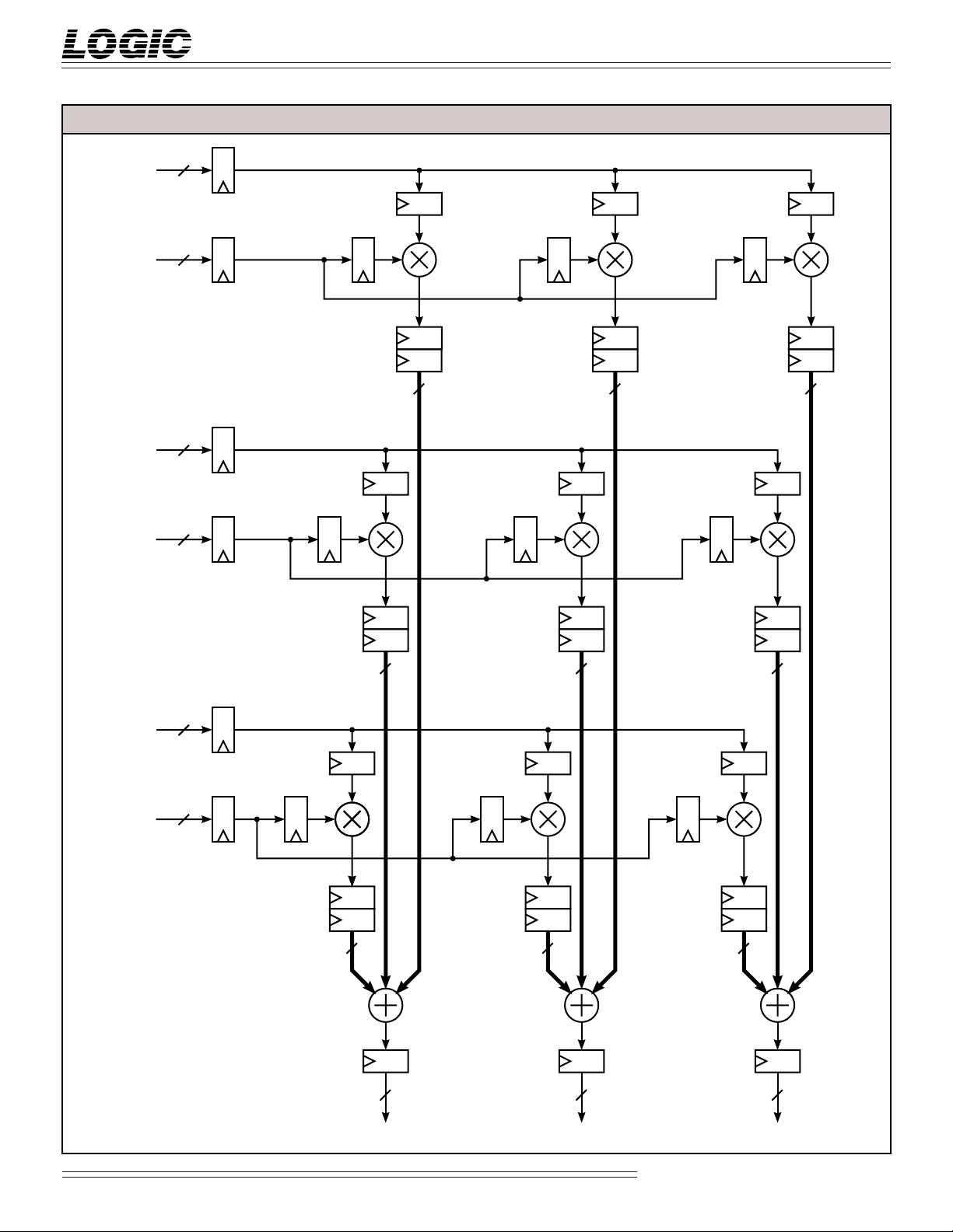
DETAILS OF OPERATION
3 x 3 Matrix Multiplier — Mode 00
In this mode, all three input ports (A,
B, C) and all three output ports (X, Y,
Z) are utilized to implement a 3 x 3
matrix multiplication (triple dot
product). Each rounded 12-bit output
is the sum of all three input words
multiplied by the appropriate coefficients (Table 5). The pipeline latency
for this mode is five clock cycles.
Therefore, the sum of products will
be output five clock cycles after the
input data has been latched. New
output data is subsequently available
every clock cycle thereafter.
(comprising of the summation of the
multiplications of the last nine data
inputs with their related coefficients)
becomes available (Table 5). The
CASIN term is also added to each
new output. The internal bus structure and pipeline delays allow new
input data to be added every cycle
while maintaining the structure of the
filtering operation. This addition of
new data every cycle produces the
effect of the convolution window
moving to the next pixel column.
4 x 2-Pixel Convolver — Mode 11
Using the A and B ports, input data is
loaded and multiplied by the onboard coefficients. These products
are then summed with the CASIN
data and rounded to create the 16-bit
output. The cascade ports allow
multiple devices to be used together
for use with larger kernels. As with
Mode 10, each cycle results in a 16-bit
output created from the products and
summations performed.
TABLE 5. LATENCY EQUATIONS
3 x 3 Matrix Multiplier — Mode 00
X(n+4) = A(n)KA1(n) + B(n)KB1(n) + C(n)KC1(n)
Y(n+4) = A(n)KA2(n) + B(n)KB2(n) + C(n)KC2(n)
Z(n+4) = A(n)KA3(n) + B(n)KB3(n) + C(n)KC3(n)
9-Tap FIR Filter — Mode 01
CASOUT(n+12) = A(n+8)KA3(n+8) + A(n+7)KA2(n+7) + A(n+6)KA1(n+6)
9-Tap FIR Filter — Mode 01
This mode utilizes the 12-bit A and B
data input ports as well as the 16-bit
CASIN port. The input data should
be presented to the A and B ports
simultaneously. The resulting 9sample response, which is half-LSB
rounded to 16 bits, begins after five
clock cycles and ends after 13 clock
cycles (Table 5). The pipeline latency
from the input of an impulse response
to the center of the output response is
nine clock cycles. The latency from
the CASIN port to the CASOUT port
is four clock cycles. New output data
is available every clock cycle.
3 x 3-Pixel Convolver — Mode 10
When configured in this mode, line
delayed data is loaded through the A,
B, and C input ports. During each
cycle, a new rounded 16-bit output
+ B(n+5)KB3(n+8) + B(n+4)KB2(n+7) + B(n+3)KB1(n+6)
+ B(n+2)KC3(n+8) + B(n+1)KC2(n+7) + B(n)KC1(n+6)
+ CASIN(n+9)
3 x 3-Pixel Convolver — Mode 10
CASOUT(n+6) = A(n+2)KA3(n+2) + A(n+1)KA2(n+1) + A(n)KA1(n)
+ B(n+2)KB3(n+2) + B(n+1)KB2(n+1) + B(n)KB1(n)
+ C(n+2)KC3(n+2) + C(n+1)KC2(n+1) + C(n)KC1(n)
+ CASIN(n+3)
4 x 2-Pixel Convolver — Mode 11
CASOUT(n+7) = A(n+3)KA3(n+3) + A(n+2)KA2(n+2) + A(n+1)KA1(n+1)
+ A(n)KC3(n+3) + B(n+3)KB3(n+3) + B(n+2)KB2(n+2)
+ B(n+1)KB1(n+1) + B(n)KC1(n+1)
+ CASIN(n+4)
Video Imaging Products
4
08/16/2000–LDS.2250-L
DEVICES INCORPORATED
FIGURE 2. 3 X 3 MATRIX MULTIPLIER — MODE 00
12
A
KA1 KA2 KA3
10
KA
21 21 21
12
B
LF2250
12 x 10-bit Matrix Multiplier
KB
KC
KB3KB2KB1
10
21 21 21
12
C
KC1 KC2 KC3
10
21 21 21
12 (MSB) 12 (MSB) 12 (MSB)
XYZ
Video Imaging Products
5
08/16/2000–LDS.2250-L

DEVICES INCORPORATED
FIGURE 3. 9-TAP FIR FILTER — MODE 01
12
A
KA1 KA2 KA3
10
KA
LF2250
12 x 10-bit Matrix Multiplier
21 21 21
KB
KC
12
B
4
KB3KB2KB1
10
3
21 21 21
KC1 KC2 KC3
10
21 21 21
CASIN
NOTE: NUMBERS IN REGISTERS INDICATE
16
NUMBER OF PIPELINE DELAYS
16
(HALF-LSB ROUNDING)
5
10000
21
2
21
16 (MSB)
CASOUT
Video Imaging Products
6
08/16/2000–LDS.2250-L

DEVICES INCORPORATED
FIGURE 4. 3 X 3-PIXEL CONVOLVER — MODE 10
12
A
KA1 KA2 KA3
10
KA
12
B
LF2250
12 x 10-bit Matrix Multiplier
21 21 21
KB
KC
KB3KB2KB1
10
21 21 21
12
C
KC1 KC2 KC3
10
21 21 21
CASIN
16
16
(HALF-LSB ROUNDING)
5
10000
21
2
21
16 (MSB)
CASOUT
Video Imaging Products
7
08/16/2000–LDS.2250-L

DEVICES INCORPORATED
FIGURE 5. 4 X 2-PIXEL CONVOLVER — MODE 11
12
A
KA1 KA2 KA3
10
KA
21 21 21
12
B
LF2250
12 x 10-bit Matrix Multiplier
3
KB
KC
KB3KB2KB1
10
21 21 21
0
KC1 KC2 KC3
10
21 21 21
CASIN
NOTE: NUMBERS IN REGISTERS INDICATE
16
NUMBER OF PIPELINE DELAYS
16
(HALF-LSB ROUNDING)
5
10000
21
2
21
16 (MSB)
CASOUT
Video Imaging Products
8
08/16/2000–LDS.2250-L

DEVICES INCORPORATED
LF2250
12 x 10-bit Matrix Multiplier
MAXIMUM RATINGS
Storage temperature ........................................................................................................... –65°C to +150°C
Operating ambient temperature........................................................................................... –55°C to +125°C
VCC supply voltage with respect to ground............................................................................ –0.5 V to +7.0V
Input signal with respect to ground ............................................................................... –0.5 V to VCC + 0.5 V
Signal applied to high impedance output ...................................................................... –0.5 V to VCC + 0.5 V
Output current into low outputs............................................................................................................. 25 mA
Latchup current ................................................................................................................ ............... > 400 mA
OPERATING CONDITIONS
Active Operation, Commercial 0°C to +70°C 4.75 V ≤ VCC ≤ 5.25 V
Active Operation, Military –55°C to +125°C 4.50 V ≤ VCC ≤ 5.50 V
ELECTRICAL CHARACTERISTICS
Above which useful life may be impaired (Notes 1, 2, 3, 8)
To meet specified electrical and switching characteristics
Mode Temperature Range (Ambient) Supply Voltage
Over Operating Conditions (Note 4)
Symbol Parameter Test Condition Min Typ Max Unit
VOH Output High Voltage Vcc = Min., IOH = –2.0 mA 2.4 V
VOL Output Low Voltage Vcc = Min., IOL = 4.0 mA 0.4 V
VIH Input High Voltage 2.0 VCC V
V IL Input Low Voltage (Note 3) 0.0 0.8 V
IIX Input Current Ground ≤ VIN ≤ VCC (Note 12) ±10 µA
IOZ Output Leakage Current (Note 12) ±40 µA
ICC1 VCC Current, Dynamic (Notes 5, 6) 160 mA
ICC2 VCC Current, Quiescent (Note 7) 12 mA
CIN Input Capacitance TA = 25°C, f = 1 MHz 10 pF
COUT Output Capacitance TA = 25°C, f = 1 MHz 10 pF
Video Imaging Products
9
08/16/2000–LDS.2250-L

DEVICES INCORPORATED
3
3
3
3
3
3
3
3
3
3
3
3
3
3
3
3
3
3
3
3
3
3
3
3
8
8
8
8
8
8
8
8
8
8
8
8
8
8
8
8
8
8
8
8
8
8
8
4
4
SWITCHING CHARACTERISTICS
LF2250
12 x 10-bit Matrix Multiplier
COMMERCIAL OPERATING RANGE (0°C to +70°C)
Symbol Parameter Min Max Min Max Min Max
tCYC Cycle Time 33 25 20
tPWL Clock Pulse Width Low 15 10 6
tPWH Clock Pulse Width High 10 10 8
tS Input Setup Time 8 6 6
tH Input Hold Time 0 0 0
tD Output Delay 18 16 15
MILITARY OPERATING RANGE (–55°C to +125°C)
Symbol Parameter Min Max Min Max
tCYC Cycle Time 33 25
tPWL Clock Pulse Width Low 15 10
tPWH Clock Pulse Width High 10 10
tS Input Setup Time 12 9
tH Input Hold Time 2 2
tD Output Delay 25 20
Notes 9, 10 (ns)
2345678901234567
2345678901234567
33
2345678901234567
2345678901234567
2345678901234567
2345678901234567
2345678901234567
2345678901234567
2345678901234567
2345678901234567
2345678901234567
2345678901234567
2345678901234567
2345678901234567
2345678901234567
2345678901234567
2345678901234567
2345678901234567
2345678901234567
2345678901234567
2345678901234567
2345678901234567
2345678901234567
Notes 9, 10 (ns)
LF2250–
*
234567890123456789012345678901212
234567890123456789012345678901212
234567890123456789012345678901212
234567890123456789012345678901212
234567890123456789012345678901212
234567890123456789012345678901212
234567890123456789012345678901212
234567890123456789012345678901212
234567890123456789012345678901212
234567890123456789012345678901212
234567890123456789012345678901212
234567890123456789012345678901212
234567890123456789012345678901212
234567890123456789012345678901212
234567890123456789012345678901212
234567890123456789012345678901212
234567890123456789012345678901212
234567890123456789012345678901212
234567890123456789012345678901212
234567890123456789012345678901212
234567890123456789012345678901212
234567890123456789012345678901212
234567890123456789012345678901212
234567890123456789012345678901212
25 20
LF2250–
*
33
25
*
2345678901234567890123
2345678901234567890123
*DISCONTINUED SPEED GRADE
10
Video Imaging Products
08/16/2000–LDS.2250-L

DEVICES INCORPORATED
SWITCHING WAVEFORMS:3 X 3 MATRIX MULTIPLIER — MODE 00
LF2250
12 x 10-bit Matrix Multiplier
CLK
CWE
KA, KB, KC
A, B, C
MODE
X11-0
Y11-0
Z11-0
1234 678
tS
1-0
01
10 11 00
tPWH
tPWL
5
tH
Kx1 Kx2 Kx3
001.0000
1-0
00
tD
KA1 + KB1 + KC1
KA2 + KB2 + KC2
KA3 + KB3 + KC3
SWITCHING WAVEFORMS: 9-TAP FIR FILTER — MODE 01
CLK
CWE
KA, KB, KC
A, B
MODE
CASIN15-0
CASOUT15-0
1 2 3 13 14 15
tS
1-0
1-0
01
Kx1 Kx2 Kx3
0 0 1.0 0
tPWH
10 11
tH
tPWL
12 16 17
0 0
01
Q13
0
0
tD
Q13KC1KC2KC3KB1
Video Imaging Products
11
08/16/2000–LDS.2250-L

DEVICES INCORPORATED
SWITCHING WAVEFORMS:3 X 3-PIXEL CONVOLVER — MODE 10
LF2250
12 x 10-bit Matrix Multiplier
123 789
61011
CLK
t
PWL
0 0
10
Q7
CWE
KA, KB, KC
A, B, C
MODE
CASIN
CASOUT
15-0
15-0
t
t
S
01
1-0
Kx1 Kx2 Kx3
0 0 1.0 0
1-0
PWH
10 11
t
H
SWITCHING WAVEFORMS:4 X 2-PIXEL CONVOLVER — MODE 11
CLK
CWE
KA, KB, KC
123 789
t
t
t
S
01
1-0
Kx1 Kx2 Kx3
PWH
10 11
t
H
PWL
61011
0
0
0
t
D
KA1 + KB1 + KC1KA2 + KB2 + KC2KA3 + KB3 + KC3
Q7
MODE
CASIN
CASOUT
A, B
15-0
15-0
0 0 1.0 0
1-0
0 0
11
0
Q8
0
0
t
D
KC1 + KC3KA1 + KB1KA2 + KB3KA3 + KB3
Q8
Video Imaging Products
12
08/16/2000–LDS.2250-L

DEVICES INCORPORATED
OE
0.2 V
t
DIS
t
ENA
0.2 V
1.5 V 1.5 V
3.0V Vth
1
Z
0
Z
Z
1
Z
0
1.5 V
1.5 V
0V Vth
VOL*
V
OH
*
V
OL
*
V
OH
*
Measured V
OL
with IOH = –10mA and IOL = 10mA
Measured V
OH
with IOH = –10mA and IOL = 10mA
S1
I
OH
I
OL
V
TH
C
L
DUT
NOTES
LF2250
12 x 10-bit Matrix Multiplier
1. Maximum Ratings indicate stress
specifications only. Functional operation of these products at values beyond those indicated in the Operating
Conditions table is not implied. Exposure to maximum rating conditions for
extended periods may affect reliability.
2. The products described by this specification include internal circuitry designed to protect the chip from damaging substrate injection currents and accumulations of static charge. Nevertheless, conventional precautions
should be observed during storage,
handling, and use of these circuits in
order to avoid exposure to excessive
electrical stress values.
3. This device provides hard clamping
of transient undershoot and overshoot.
Input levels below ground or above VCC
will be clamped beginning at –0.6 V and
VCC + 0.6 V. The device can withstand
indefinite operation with inputs in the
range of –0.5 V to +7.0 V. Device operation will not be adversely affected, however, input current levels will be well in
excess of 100 mA.
9. AC specifications are tested with
input transition times less than 3 ns,
output reference levels of 1.5 V (except
tDIS test), and input levels of nominally
0 to 3.0 V. Output loading may be a
resistive divider which provides for
specified IOH and IOL at an output
voltage of VOH min and VOL max
respectively. Alternatively, a diode
bridge with upper and lower current
sources of IOH and IOL respectively,
and a balancing voltage of 1.5 V may be
used. Parasitic capacitance is 30 pF
minimum, and may be distributed.
This device has high-speed outputs capable of large instantaneous current
pulses and fast turn-on/turn-off times.
As a result, care must be exercised in the
testing of this device. The following
measures are recommended:
a. A 0.1 µF ceramic capacitor should be
installed between VCC and Ground
leads as close to the Device Under Test
(DUT) as possible. Similar capacitors
should be installed between device VCC
and the tester common, and device
ground and tester common.
11. For the tENA test, the transition is
measured to the 1.5 V crossing point
with datasheet loads. For the tDIS test,
the transition is measured to the
±200mV level from the measured
steady-state output voltage with
±10mA loads. The balancing voltage, VTH, is set at 3.5 V for Z-to-0
and 0-to-Z tests, and set at 0 V for Zto-1 and 1-to-Z tests.
12. These parameters are only tested at
the high temperature extreme, which is
the worst case for leakage current.
FIGURE A. OUTPUT LOADING CIRCUIT
FIGURE B. THRESHOLD LEVELS
4. Actual test conditions may vary
from those designated but operation is
guaranteed as specified.
5. Supply current for a given application can be accurately approximated
by:
2
NCV F
4
where
N = total number of device outputs
C = capacitive load per output
V = supply voltage
F = clock frequency
6. Tested with all outputs changing every cycle and no load, at a 20 MHz clock
rate.
7. Tested with all inputs within 0.1 V of
VCC or Ground, no load.
8. These parameters are guaranteed
but not 100% tested.
b. Ground and VCC supply planes
must be brought directly to the DUT
socket or contactor fingers.
c. Input voltages should be adjusted to
compensate for inductive ground and VCC
noise to maintain required DUT input
levels relative to the DUT ground pin.
10. Each parameter is shown as a minimum or maximum value. Input requirements are specified from the point
of view of the external system driving
the chip. Setup time, for example, is
specified as a minimum since the external system must supply at least that
much time to meet the worst-case requirements of all parts. Responses
from the internal circuitry are specified
from the point of view of the device.
Output delay, for example, is specified
as a maximum since worst-case operation of any device always provides data
within that time.
13
Video Imaging Products
08/16/2000–LDS.2250-L

DEVICES INCORPORATED
ORDERING INFORMATION
ORDERING INFORMATION
120-pin
XC7XC8VCCXC9XC10XC11GND
MODE0MODE1C11C10C9C8C7GND
12 x 10-bit Matrix Multiplier
C6C5C4VCCC3C2C1C0B11B10B9B8B7B6B
LF2250
5
XC
XC
XC
XC
XC
XC
XC
GND
YC
YC
YC
V
YC
GND
YC
V
YC
YC
YC
GND
ZC
ZC
ZC
ZC
ZC
ZC
120
119
118
117
116
115
114
113
112
111
110
109
108
107
106
105
104
CC
KC7KC8KC
V
103
6
1
5
2
4
3
3
4
2
5
1
6
0
7
8
11
9
10
10
9
11
CC
12
8
13
Y
7
14
Y
6
15
16
5
Y
17
Y
4
18
0
19
CC
20
1
21
2
22
3
23
24
0
25
1
26
2
27
3
28
4
29
5
30
3132333435363738394041424344454647484950515253545556575859
8
9
11
GND
ZC
ZC10ZC
KC0KC1KC2KC
ZC6ZC7ZC
3
GND
Top
View
4KC5KC6
KC
999897969594939291
102
101
100
9
KB0KB1KB2KB3KB4KB5KB6KB7KB8KB9KA
90
B
89
88
87
86
85
84
83
82
81
80
79
78
77
76
75
74
73
72
71
70
69
68
67
66
65
64
63
62
61
60
0
4
B
3
CLK
2
B
B
1
B
0
A
11
A
10
A
9
A
8
A
7
A
6
A
5
A
4
A
3
A
2
A
1
A
0
GND
CWE
CWE
KA
KA
KA
KA
KA
KA
KA
KA
KA
0
1
9
8
7
6
5
4
3
2
1
Speed
25 ns
20 ns
0°C to +70°C — COMMERCIAL SCREENING
0°C to +70°C — COMMERCIAL SCREENING
–55°C to +125°C — COMMERCIAL SCREENING
–40°C to +85°C — COMMERCIAL SCREENING
–55°C to +125°C — MIL-STD-883 COMPLIANT
–55°C to +125°C — MIL-STD-883 COMPLIANT
Plastic Quad Flatpack
(Q1)
LF2250QC25
LF2250QC20
Video Imaging Products
14
08/16/2000–LDS.2250-L

DEVICES INCORPORATED
1
1
1
1
1
1
1
1
1
1
1
1
1
1
1
1
1
1
1
1
1
1
1
1
1
1
1
1
1
1
1
1
1
1
1
1
1
1
1
1
1
1
1
1
1
1
1
1
1
1
1
1
1
1
1
1
1
1
1
1
1
1
1
1
1
1
1
12 x 10-bit Matrix Multiplier
ORDERING INFORMATION
23456789012345678901234567890121234567890123456789012345678901212345678901234567890123456789012
23456789012345678901234567890121234567890123456789012345678901212345678901234567890123456789012
23456789012345678901234567890121234567890123456789012345678901212345678901234567890123456789012
120-pin
23456789012345678901234567890121234567890123456789012345678901212345678901234567890123456789012
23456789012345678901234567890121234567890123456789012345678901212345678901234567890123456789012
23456789012345678901234567890121234567890123456789012345678901212345678901234567890123456789012
23456789012345678901234567890121234567890123456789012345678901212345678901234567890123456789012
23456789012345678901234567890121234567890123456789012345678901212345678901234567890123456789012
23456789012345678901234567890121234567890123456789012345678901212345678901234567890123456789012
23456789012345678901234567890121234567890123456789012345678901212345678901234567890123456789012
23456789012345678901234567890121234567890123456789012345678901212345678901234567890123456789012
23456789012345678901234567890121234567890123456789012345678901212345678901234567890123456789012
23456789012345678901234567890121234567890123456789012345678901212345678901234567890123456789012
23456789012345678901234567890121234567890123456789012345678901212345678901234567890123456789012
23456789012345678901234567890121234567890123456789012345678901212345678901234567890123456789012
23456789012345678901234567890121234567890123456789012345678901212345678901234567890123456789012
23456789012345678901234567890121234567890123456789012345678901212345678901234567890123456789012
23456789012345678901234567890121234567890123456789012345678901212345678901234567890123456789012
23456789012345678901234567890121234567890123456789012345678901212345678901234567890123456789012
23456789012345678901234567890121234567890123456789012345678901212345678901234567890123456789012
23456789012345678901234567890121234567890123456789012345678901212345678901234567890123456789012
23456789012345678901234567890121234567890123456789012345678901212345678901234567890123456789012
23456789012345678901234567890121234567890123456789012345678901212345678901234567890123456789012
23456789012345678901234567890121234567890123456789012345678901212345678901234567890123456789012
23456789012345678901234567890121234567890123456789012345678901212345678901234567890123456789012
23456789012345678901234567890121234567890123456789012345678901212345678901234567890123456789012
23456789012345678901234567890121234567890123456789012345678901212345678901234567890123456789012
23456789012345678901234567890121234567890123456789012345678901212345678901234567890123456789012
23456789012345678901234567890121234567890123456789012345678901212345678901234567890123456789012
23456789012345678901234567890121234567890123456789012345678901212345678901234567890123456789012
23456789012345678901234567890121234567890123456789012345678901212345678901234567890123456789012
23456789012345678901234567890121234567890123456789012345678901212345678901234567890123456789012
23456789012345678901234567890121234567890123456789012345678901212345678901234567890123456789012
23456789012345678901234567890121234567890123456789012345678901212345678901234567890123456789012
23456789012345678901234567890121234567890123456789012345678901212345678901234567890123456789012
23456789012345678901234567890121234567890123456789012345678901212345678901234567890123456789012
23456789012345678901234567890121234567890123456789012345678901212345678901234567890123456789012
23456789012345678901234567890121234567890123456789012345678901212345678901234567890123456789012
23456789012345678901234567890121234567890123456789012345678901212345678901234567890123456789012
23456789012345678901234567890121234567890123456789012345678901212345678901234567890123456789012
23456789012345678901234567890121234567890123456789012345678901212345678901234567890123456789012
23456789012345678901234567890121234567890123456789012345678901212345678901234567890123456789012
23456789012345678901234567890121234567890123456789012345678901212345678901234567890123456789012
23456789012345678901234567890121234567890123456789012345678901212345678901234567890123456789012
23456789012345678901234567890121234567890123456789012345678901212345678901234567890123456789012
23456789012345678901234567890121234567890123456789012345678901212345678901234567890123456789012
23456789012345678901234567890121234567890123456789012345678901212345678901234567890123456789012
23456789012345678901234567890121234567890123456789012345678901212345678901234567890123456789012
23456789012345678901234567890121234567890123456789012345678901212345678901234567890123456789012
23456789012345678901234567890121234567890123456789012345678901212345678901234567890123456789012
23456789012345678901234567890121234567890123456789012345678901212345678901234567890123456789012
23456789012345678901234567890121234567890123456789012345678901212345678901234567890123456789012
23456789012345678901234567890121234567890123456789012345678901212345678901234567890123456789012
23456789012345678901234567890121234567890123456789012345678901212345678901234567890123456789012
23456789012345678901234567890121234567890123456789012345678901212345678901234567890123456789012
23456789012345678901234567890121234567890123456789012345678901212345678901234567890123456789012
23456789012345678901234567890121234567890123456789012345678901212345678901234567890123456789012
23456789012345678901234567890121234567890123456789012345678901212345678901234567890123456789012
23456789012345678901234567890121234567890123456789012345678901212345678901234567890123456789012
23456789012345678901234567890121234567890123456789012345678901212345678901234567890123456789012
23456789012345678901234567890121234567890123456789012345678901212345678901234567890123456789012
23456789012345678901234567890121234567890123456789012345678901212345678901234567890123456789012
23456789012345678901234567890121234567890123456789012345678901212345678901234567890123456789012
23456789012345678901234567890121234567890123456789012345678901212345678901234567890123456789012
23456789012345678901234567890121234567890123456789012345678901212345678901234567890123456789012
23456789012345678901234567890121234567890123456789012345678901212345678901234567890123456789012
23456789012345678901234567890121234567890123456789012345678901212345678901234567890123456789012
M
Speed
0°C to +70°C — COMMERCIAL SCREENING
–55°C to +125°C — COMMERCIAL SCREENING
–55°C to +125°C — MIL-STD-883 COMPLIANT
12345
A
XC
9
XC
7
XC
B
XC
5
XC
4
XC
C
XC
2
XC
1
XC
D
XC
0
YC
11
XC
E
YC
10
YC
9
GND
F
YC
8
Y
7
V
G
Y
6
Y
5
GND
H
V
YC
0
Y
4
J
YC
2
YC
1
GND
K
ZC
YC
0
3
ZC
L
ZC
4
ZC
ZC
7
ZC
ZC
ZC
1
2
N
ZC
8
ZC
5
ZC
6
MODE
0
C
11
C
1
C
C
KEY
8
9
10
GND
Top View
CC
10
XC
11
MODE
8
V
CC
6
GND
3
Through Package
(i.e., Component Side Pinout)
CC
3
GND
6
ZC
9
KC
10
0
GND
KC
11
KC
2
4
KC
1
KC
3
KC
5
Discontinued Package
Ceramic Pin Grid Array
(G4)
15
7 8 9 10 11
C
7
C
5
C
3
C
1
C
6
C
4
C
2
B
11
V
CC
C
0
B
8
CC
KB
0
KB
V
KC
KC
6
KC
7
KC
4
KB
8
9
KB
2
KB
5
8
KB
1
KB
3
12 13
B
10
B
7
B
4
B
9
B
6
B
2
B
5
B
3
B
1
CLK
B
0
A
10
A
11
A
9
A
8
A
7
A
6
A
5
A
3
A
2
A
4
GND
A
0
A
1
8
CWE
1
CWE
KA
KA
4
KA
KA
1
KA
KB
9
KA
KB
6
KB
Video Imaging Products
0
7
KA
9
5
KA
6
2
KA
3
7
KA
0
LF2250
08/16/2000–LDS.2250-L
 Loading...