DEVICES INCORPORATED
LF2249
12 x 12-bit Digital Mixer
LF2249
DEVICES INCORPORATED
FEATURES
❑❑
❑ 40 MHz Data and Computation Rate
❑❑
❑❑
❑ Two 12 x 12-bit Multipliers with
❑❑
Individual Data Inputs
❑❑
❑ Separate 16-bit Input Port for
❑❑
Cascading Devices
❑❑
❑ Independent, User-Selectable 1–16
❑❑
Clock Pipeline Delay for Each Data
Input
❑❑
❑ User-Selectable Rounding of Products
❑❑
❑❑
❑ Fully Registered, Pipelined
❑❑
Architecture
❑❑
❑ Three-State Outputs
❑❑
❑❑
❑ Fully TTL Compatible
❑❑
❑❑
❑ Replaces TRW/Raytheon/Fairchild
❑❑
TMC2249
❑❑
❑ 120-pin PQFP
❑❑
12 x 12-bit Digital Mixer
DESCRIPTION
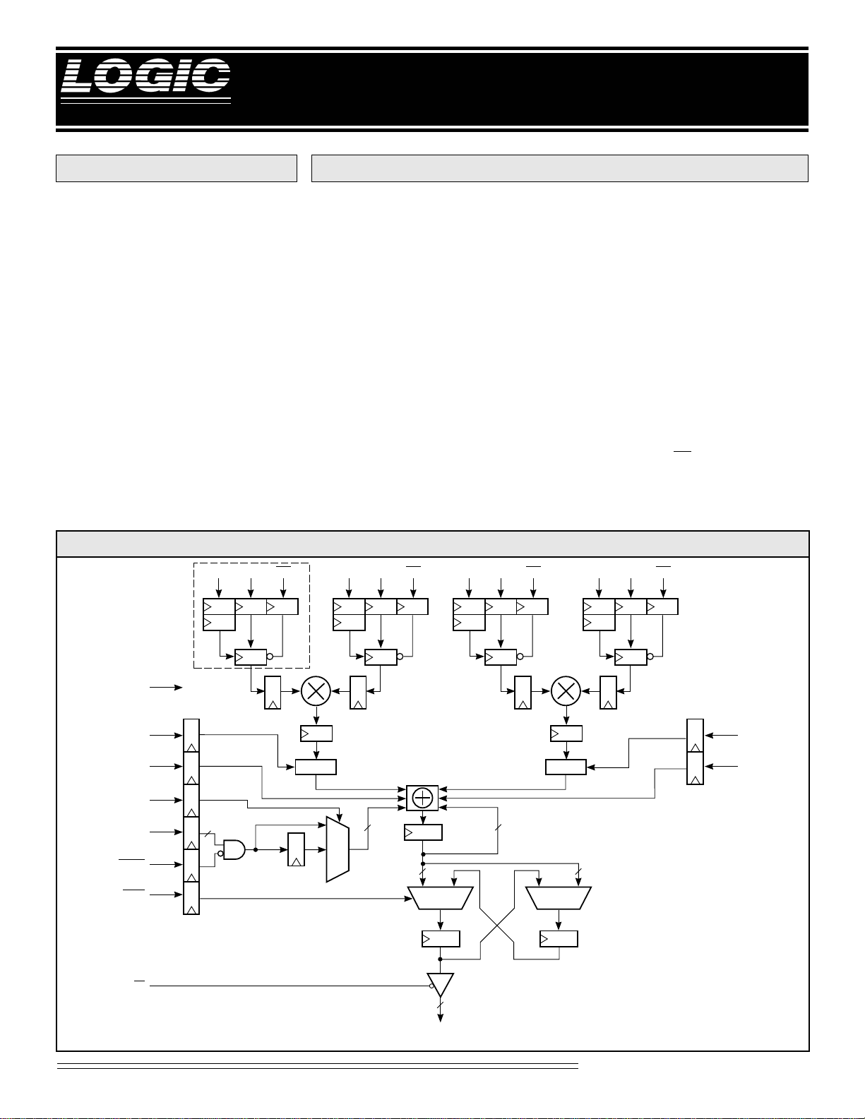
The LF2249 is a high-speed digital
mixer comprised of two 12-bit
multipliers and a 24-bit accumulator.
All multiplier inputs are user accessible, and each can be updated on
every clock cycle. The LF2249 utilizes
a pipelined architecture with fully
registered inputs and outputs and an
asynchronous three-state output
enable control for optimum flexibility.
Independent input register clock
enables allow the user to hold the
data inputs over multiple clock cycles.
Each multiplier input also includes a
user-selectable 1-16 clock pipeline
delay. The output of each multiplier
can be independently negated under
user control for subtraction of products. The sum of the products can
also be internally rounded to 16 bits
during the accumulation process.
A separate 16-bit input port connected to the accumulator is included
to allow cascading of multiple
LF2249s. Access to all 24 bits of the
accumulator is gained by switching
between upper or lower 16-bit words.
The accumulated output data is
updated on every clock cycle.
All inputs and outputs of the LF2249
are registered on the rising edge of
clock, except for OE. Internal pipeline
registers for all data and control
inputs are provided to maintain
1
2
3
4
5
6
LF2249 BLOCK DIAGRAM
ADEL
3-0A11-0
CLK
NEG
RND
CAS
15-0
CASEN
SWAP
1
FT
4
4
16
ENA BDEL
1–16 1–16
2's COMP
3
3-0B11-0
16
2 : 1
ENB
CDEL
3-0C11-0
16
10 0 1
2 : 1
ENC DDEL
1–16 1–16
2's COMP
24
16MS LS
2 : 1
3-0D11-0
END
7
8
9
4
4
NEG
ACC
2
10
11
OE
NOTE: NUMBERS IN REGISTERS INDICATED
NUMBER OF PIPELINE DELAYS.
16
S
15-0
Video Imaging Products
1
08/16/2000–LDS.2249-J

DEVICES INCORPORATED
15 14 13 10 9 81211 76543210
–2
23222221
2182172
16
2202
19
215214213212211210292
8
(Sign)
15 14 13 10 9 81211 76543210
–2
23222221
2182172
16
2202
19
215214213212211210292
8
(Sign)
LF2249
12 x 12-bit Digital Mixer
synchronous operation between the
incoming data and all available
control functions. The LF2249 operates at a clock rate of 40 MHz over the
full commercial temperature and
supply voltage ranges.
Because of its flexibility, the LF2249 is
ideally suited for applications such as
image switching and mixing, digital
quadrature mixing and modulating,
FIR filtering, and arithmetic function
and waveform synthesis.
SIGNAL DEFINITIONS
Power
VCC and GND
+5 V power supply. All pins must be
connected.
Clock
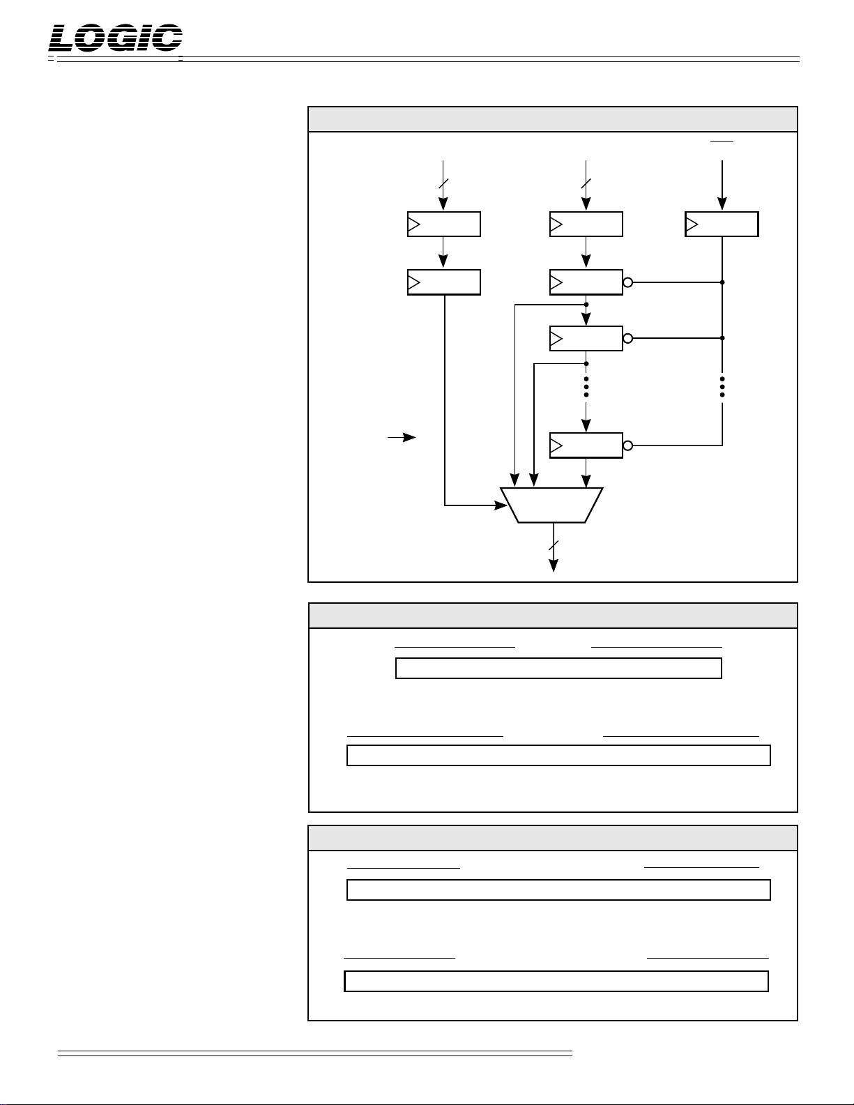
DETAILED VIEW OF BLOCK DIAGRAM OUTLINED AREA
ADEL
3-0
4 12
CLK
16 : 1
A
R
11-0
1
R
R
2
16
ENA
CLK — Master Clock
The rising edge of CLK strobes all enabled registers. All timing specifications are referenced to the rising edge of
CLK.
Inputs
A11-0–D11-0 — Data Inputs
A11-0–D11-0 are 12-bit data input registers. Data is latched into the input registers on the rising edge of CLK. The
contents of the input registers are
clocked into the top of the corresponding 16-stage pipeline delay (pushing the
contents of the register stack down one
register position) on the next clock cycle
if the pipeline register stack is enabled.
The LSBs are A0-D0 (Figure 1a).
CAS15-0 — Cascade Data Input
CAS15-0 is the 16-bit cascade data input
port. Data is latched into the register on
the rising edge of CLK. The LSB is CAS0
(Figure 1a).
12
FIGURE 1A.INPUT FORMATS
Data Input
10 9 811 76543210
11
–2
(Sign)
210292
8
272625242322212
Cascade Input
FIGURE 1B.OUTPUT FORMATS
Sum Output (Upper 16 bits)
Sum Output (Lower 16 bits)
15 14 13 10 9 81211 76543210
15214213
2
2122
11
210292
8
272625242322212
0
0
Video Imaging Products
2
08/16/2000–LDS.2249-J

DEVICES INCORPORATED
LF2249
12 x 12-bit Digital Mixer
Outputs
S15-0 — Data Output
The current 16-bit result is available
on the S15-0 outputs. The output data
may be either the upper or lower 16
bits of the accumulator output, depending on the state of SWAP. The
LSB is S0 (Figure 1b).
Controls
ENA–END — Pipeline Register Enable
Input data in the N (N = A, B, C, or D)
input register is latched into the corresponding pipeline register stack on
each rising edge of CLK for which ENN
is LOW. Data already in the N register
stack is pushed down one register position. When ENN is HIGH, the data in
the N pipeline register stack does not
change, and the data in the N input
register will not be stored in the register
stack.
ADEL3-0–DDEL3-0 — Pipeline Delay
Select
NDEL (N = A, B, C, or D) is the 4-bit
registered pipeline delay select word.
NDEL determines which stage of the N
pipeline register stack is routed to the
multiplier inputs. The minimum delay
is one clock cycle (NDEL = 0000), and
the maximum delay is 16 clock cycle
(NDEL = 1111). Upon power up, the
values of ADEL–DDEL and the contents of the pipeline register stacks are
unknown and must be initialized by the
user.
NEG1–NEG2 — Negate Control
The NEG1 and NEG2 controls determine whether a subtraction or accumulation of products is performed. When
NEG1 is HIGH, the product A x B is
negated, causing the product to be subtracted from the accumulator contents.
Likewise, when NEG2 is HIGH, the
product C x D is negated, causing the
product to be subtracted as well. NEG1
and NEG2 determine the operation to
be performed on the data input during
the current clock cycle when ADEL–
DDEL = 0000.
CASEN — Cascade Enable
When CASEN is LOW, data being input on the CAS15-0 inputs during that
clock cycle will be registered and accumulated internally. When CASEN is
HIGH, the CAS15-0 inputs are ignored.
FT — Feedthrough Control
When FT is LOW and ADEL–DDEL =
0000, data being input on the CAS15-0
inputs is delayed three clock cycles to
align the data with the data being input
on the A11-0–D11-0 inputs. When FT is
HIGH, the cascade data being input is
routed around the three delay registers
to simplify the cascading of multiple
devices.
ACC — Accumulator Control
The ACC input determines whether internal accumulation is performed on
the data input during the current clock
cycle. If ACC is LOW, no accumulation
is performed, the prior accumulated
sum is cleared, and the current sum of
products is output. When ACC is
HIGH, the emerging products are
added to the sum of the previous products.
RND — Rounding Control
When RND is HIGH, the sum of the
products of the data being input on
the current clock cycle will be
rounded to 16 bits. To avoid the accumulation of roundoff errors, rounding is only performed during the first
cycle of each accumulation process.
SWAP — Output Select
The SWAP control allows the user to
access all 24 bits of the accumulator
output by switching between upper
and lower 16-bit words. When SWAP
is HIGH, the upper 16 bits of the accumulator are always output. When
SWAP is LOW, the lower 16 bits of the
accumulator are output on every
other clock cycle. As long as SWAP
remains LOW, new output data will
not be clocked into the output registers.
OE — Output Enable
When the OE signal is LOW, the
current data in the output registers
is available on the S15-0 pins. When
OE is HIGH, the outputs are in a
high-impedance state.
1
2
3
4
5
6
7
8
9
10
11
Video Imaging Products
3
08/16/2000–LDS.2249-J
 Loading...