

DEVICES INCORPORATED
LF2249
12 x 12-bit Digital Mixer
LF2249
DEVICES INCORPORATED
FEATURES
❑❑
❑ 40 MHz Data and Computation Rate
❑❑
❑❑
❑ Two 12 x 12-bit Multipliers with
❑❑
Individual Data Inputs
❑❑
❑ Separate 16-bit Input Port for
❑❑
Cascading Devices
❑❑
❑ Independent, User-Selectable 1–16
❑❑
Clock Pipeline Delay for Each Data
Input
❑❑
❑ User-Selectable Rounding of Products
❑❑
❑❑
❑ Fully Registered, Pipelined
❑❑
Architecture
❑❑
❑ Three-State Outputs
❑❑
❑❑
❑ Fully TTL Compatible
❑❑
❑❑
❑ Replaces TRW/Raytheon/Fairchild
❑❑
TMC2249
❑❑
❑ 120-pin PQFP
❑❑
12 x 12-bit Digital Mixer
DESCRIPTION
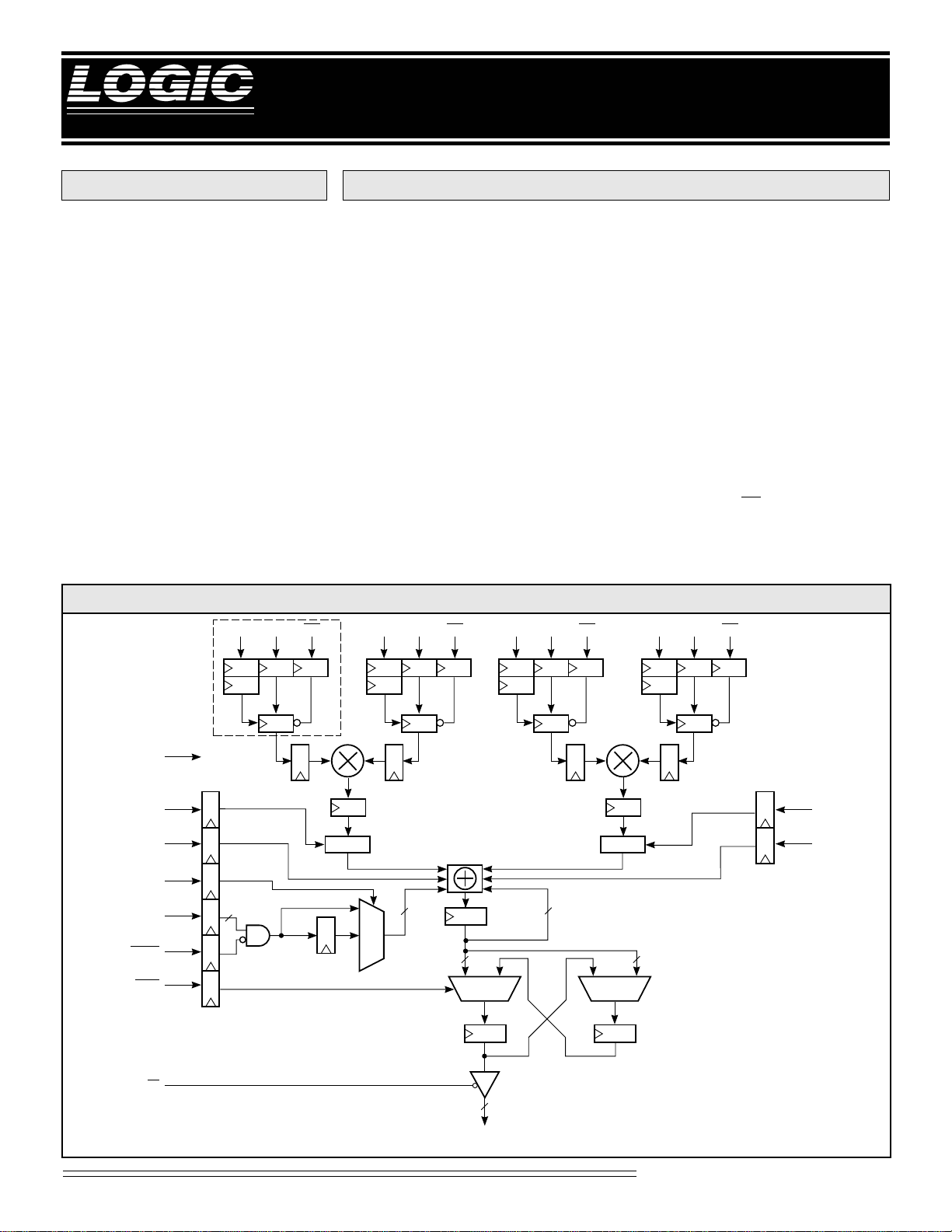
The LF2249 is a high-speed digital
mixer comprised of two 12-bit
multipliers and a 24-bit accumulator.
All multiplier inputs are user accessible, and each can be updated on
every clock cycle. The LF2249 utilizes
a pipelined architecture with fully
registered inputs and outputs and an
asynchronous three-state output
enable control for optimum flexibility.
Independent input register clock
enables allow the user to hold the
data inputs over multiple clock cycles.
Each multiplier input also includes a
user-selectable 1-16 clock pipeline
delay. The output of each multiplier
can be independently negated under
user control for subtraction of products. The sum of the products can
also be internally rounded to 16 bits
during the accumulation process.
A separate 16-bit input port connected to the accumulator is included
to allow cascading of multiple
LF2249s. Access to all 24 bits of the
accumulator is gained by switching
between upper or lower 16-bit words.
The accumulated output data is
updated on every clock cycle.
All inputs and outputs of the LF2249
are registered on the rising edge of
clock, except for OE. Internal pipeline
registers for all data and control
inputs are provided to maintain
1
2
3
4
5
6
LF2249 BLOCK DIAGRAM
ADEL
3-0A11-0
CLK
NEG
RND
CAS
15-0
CASEN
SWAP
1
FT
4
4
16
ENA BDEL
1–16 1–16
2's COMP
3
3-0B11-0
16
2 : 1
ENB
CDEL
3-0C11-0
16
10 0 1
2 : 1
ENC DDEL
1–16 1–16
2's COMP
24
16MS LS
2 : 1
3-0D11-0
END
7
8
9
4
4
NEG
ACC
2
10
11
OE
NOTE: NUMBERS IN REGISTERS INDICATED
NUMBER OF PIPELINE DELAYS.
16
S
15-0
Video Imaging Products
1
08/16/2000–LDS.2249-J
DEVICES INCORPORATED
15 14 13 10 9 81211 76543210
–2
23222221
2182172
16
2202
19
215214213212211210292
8
(Sign)
15 14 13 10 9 81211 76543210
–2
23222221
2182172
16
2202
19
215214213212211210292
8
(Sign)
LF2249
12 x 12-bit Digital Mixer
synchronous operation between the
incoming data and all available
control functions. The LF2249 operates at a clock rate of 40 MHz over the
full commercial temperature and
supply voltage ranges.
Because of its flexibility, the LF2249 is
ideally suited for applications such as
image switching and mixing, digital
quadrature mixing and modulating,
FIR filtering, and arithmetic function
and waveform synthesis.
SIGNAL DEFINITIONS
Power
VCC and GND
+5 V power supply. All pins must be
connected.
Clock
DETAILED VIEW OF BLOCK DIAGRAM OUTLINED AREA
ADEL
3-0
4 12
CLK
16 : 1
A
R
11-0
1
R
R
2
16
ENA
CLK — Master Clock
The rising edge of CLK strobes all enabled registers. All timing specifications are referenced to the rising edge of
CLK.
Inputs
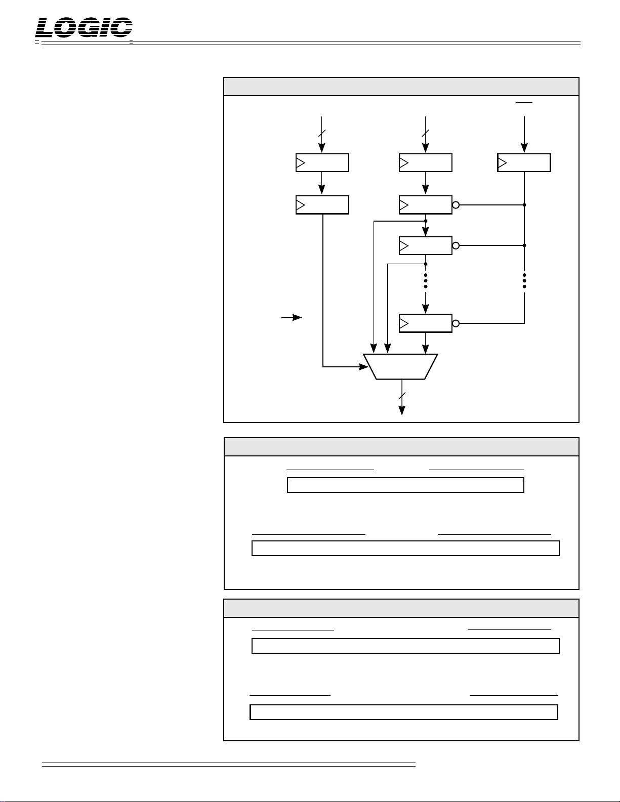
A11-0–D11-0 — Data Inputs
A11-0–D11-0 are 12-bit data input registers. Data is latched into the input registers on the rising edge of CLK. The
contents of the input registers are
clocked into the top of the corresponding 16-stage pipeline delay (pushing the
contents of the register stack down one
register position) on the next clock cycle
if the pipeline register stack is enabled.
The LSBs are A0-D0 (Figure 1a).
CAS15-0 — Cascade Data Input
CAS15-0 is the 16-bit cascade data input
port. Data is latched into the register on
the rising edge of CLK. The LSB is CAS0
(Figure 1a).
12
FIGURE 1A.INPUT FORMATS
Data Input
10 9 811 76543210
11
–2
(Sign)
210292
8
272625242322212
Cascade Input
FIGURE 1B.OUTPUT FORMATS
Sum Output (Upper 16 bits)
Sum Output (Lower 16 bits)
15 14 13 10 9 81211 76543210
15214213
2
2122
11
210292
8
272625242322212
0
0
Video Imaging Products
2
08/16/2000–LDS.2249-J

DEVICES INCORPORATED
LF2249
12 x 12-bit Digital Mixer
Outputs
S15-0 — Data Output
The current 16-bit result is available
on the S15-0 outputs. The output data
may be either the upper or lower 16
bits of the accumulator output, depending on the state of SWAP. The
LSB is S0 (Figure 1b).
Controls
ENA–END — Pipeline Register Enable
Input data in the N (N = A, B, C, or D)
input register is latched into the corresponding pipeline register stack on
each rising edge of CLK for which ENN
is LOW. Data already in the N register
stack is pushed down one register position. When ENN is HIGH, the data in
the N pipeline register stack does not
change, and the data in the N input
register will not be stored in the register
stack.
ADEL3-0–DDEL3-0 — Pipeline Delay
Select
NDEL (N = A, B, C, or D) is the 4-bit
registered pipeline delay select word.
NDEL determines which stage of the N
pipeline register stack is routed to the
multiplier inputs. The minimum delay
is one clock cycle (NDEL = 0000), and
the maximum delay is 16 clock cycle
(NDEL = 1111). Upon power up, the
values of ADEL–DDEL and the contents of the pipeline register stacks are
unknown and must be initialized by the
user.
NEG1–NEG2 — Negate Control
The NEG1 and NEG2 controls determine whether a subtraction or accumulation of products is performed. When
NEG1 is HIGH, the product A x B is
negated, causing the product to be subtracted from the accumulator contents.
Likewise, when NEG2 is HIGH, the
product C x D is negated, causing the
product to be subtracted as well. NEG1
and NEG2 determine the operation to
be performed on the data input during
the current clock cycle when ADEL–
DDEL = 0000.
CASEN — Cascade Enable
When CASEN is LOW, data being input on the CAS15-0 inputs during that
clock cycle will be registered and accumulated internally. When CASEN is
HIGH, the CAS15-0 inputs are ignored.
FT — Feedthrough Control
When FT is LOW and ADEL–DDEL =
0000, data being input on the CAS15-0
inputs is delayed three clock cycles to
align the data with the data being input
on the A11-0–D11-0 inputs. When FT is
HIGH, the cascade data being input is
routed around the three delay registers
to simplify the cascading of multiple
devices.
ACC — Accumulator Control
The ACC input determines whether internal accumulation is performed on
the data input during the current clock
cycle. If ACC is LOW, no accumulation
is performed, the prior accumulated
sum is cleared, and the current sum of
products is output. When ACC is
HIGH, the emerging products are
added to the sum of the previous products.
RND — Rounding Control
When RND is HIGH, the sum of the
products of the data being input on
the current clock cycle will be
rounded to 16 bits. To avoid the accumulation of roundoff errors, rounding is only performed during the first
cycle of each accumulation process.
SWAP — Output Select
The SWAP control allows the user to
access all 24 bits of the accumulator
output by switching between upper
and lower 16-bit words. When SWAP
is HIGH, the upper 16 bits of the accumulator are always output. When
SWAP is LOW, the lower 16 bits of the
accumulator are output on every
other clock cycle. As long as SWAP
remains LOW, new output data will
not be clocked into the output registers.
OE — Output Enable
When the OE signal is LOW, the
current data in the output registers
is available on the S15-0 pins. When
OE is HIGH, the outputs are in a
high-impedance state.
1
2
3
4
5
6
7
8
9
10
11
Video Imaging Products
3
08/16/2000–LDS.2249-J

DEVICES INCORPORATED
LF2249
12 x 12-bit Digital Mixer
MAXIMUM RATINGS
Storage temperature ........................................................................................................... –65°C to +150°C
Operating ambient temperature........................................................................................... –55°C to +125°C
VCC supply voltage with respect to ground............................................................................ –0.5 V to +7.0V
Input signal with respect to ground ............................................................................... –0.5 V to VCC + 0.5 V
Signal applied to high impedance output ...................................................................... –0.5 V to VCC + 0.5 V
Output current into low outputs............................................................................................................. 25 mA
Latchup current ............................................................................................................................... > 400 mA
OPERATING CONDITIONS
Active Operation, Commercial 0°C to +70°C 4.75 V ≤ VCC ≤ 5.25 V
Active Operation, Military –55°C to +125°C 4.50 V ≤ VCC ≤ 5.50V
ELECTRICAL CHARACTERISTICS
Above which useful life may be impaired (Notes 1, 2, 3, 8)
To meet specified electrical and switching characteristics
Mode Temperature Range (Ambient) Supply Voltage
Over Operating Conditions (Note 4)
Symbol Parameter Test Condition Min Typ Max Unit
VOH Output High Voltage Vcc = Min., IOH = –2.0 mA 2.4 V
VOL Output Low Voltage Vcc = Min., IOL = 4.0 mA 0.4 V
VIH Input High Voltage 2.0 VCC V
VIL Input Low Voltage (Note 3) 0.0 0.8 V
IIX Input Current Ground ≤ VIN ≤ VCC (Note 12) ±10 µA
IOZ Output Leakage Current (Note 12) ±40 µA
ICC1 VCC Current, Dynamic (Notes 5, 6) 100 mA
ICC2 VCC Current, Quiescent (Note 7) 6mA
CIN Input Capacitance T A = 25°C, f = 1 MHz 10 pF
COUT Output Capacitance TA = 25°C, f = 1 MHz 10 pF
Video Imaging Products
4
08/16/2000–LDS.2249-J

DEVICES INCORPORATED
2
2
2
2
2
2
2
2
2
2
2
2
2
2
2
2
2
2
2
2
2
2
2
2
2
2
2
2
2
2
7
7
7
7
7
7
7
7
7
7
7
7
7
7
7
7
7
7
7
7
7
7
7
7
7
7
7
7
7
7
4
SWITCHING CHARACTERISTICS
LF2249
12 x 12-bit Digital Mixer
COMMERCIAL OPERATING RANGE (0°C to +70°C)
Symbol Parameter Min Max Min Max Min Max
tCYC Cycle Time 40 33 25
tPWL Clock Pulse Width, LOW 15 15 10
tPWH Clock Pulse Width, HIGH 10 10 10
tS Input Setup Time 8 8 7
tH Input Hold Time 0 0 0
tD Output Delay 17 15 14
tENA Three-State Output Enable Delay (Note 11) 15 15 15
tDIS Three-State Output Disable Delay (Note 11) 15 15 15
MILITARY OPERATING RANGE (–55°C to +125°C)
Symbol Parameter Min Max Min Max
tCYC Cycle Time 40 33
tPWL Clock Pulse Width, LOW 15 15
tPWH Clock Pulse Width, HIGH 10 10
tS Input Setup Time 8 8
tH Input Hold Time 0 0
tD Output Delay 17 15
tENA Three-State Output Enable Delay (Note 11) 15 15
tDIS Three-State Output Disable Delay (Note 11) 15 15
Notes 9, 10 (ns)
234567890123456
234567890123456
234567890123456
234567890123456
234567890123456
234567890123456
234567890123456
234567890123456
234567890123456
234567890123456
234567890123456
234567890123456
234567890123456
234567890123456
234567890123456
234567890123456
234567890123456
234567890123456
234567890123456
234567890123456
234567890123456
234567890123456
234567890123456
234567890123456
234567890123456
234567890123456
234567890123456
234567890123456
234567890123456
234567890123456
Notes 9, 10 (ns)
40
LF2249-
*
234567890123456789012345678901
234567890123456789012345678901
234567890123456789012345678901
234567890123456789012345678901
234567890123456789012345678901
234567890123456789012345678901
234567890123456789012345678901
234567890123456789012345678901
234567890123456789012345678901
234567890123456789012345678901
234567890123456789012345678901
234567890123456789012345678901
234567890123456789012345678901
234567890123456789012345678901
234567890123456789012345678901
234567890123456789012345678901
234567890123456789012345678901
234567890123456789012345678901
234567890123456789012345678901
234567890123456789012345678901
234567890123456789012345678901
234567890123456789012345678901
234567890123456789012345678901
234567890123456789012345678901
234567890123456789012345678901
234567890123456789012345678901
234567890123456789012345678901
234567890123456789012345678901
234567890123456789012345678901
234567890123456789012345678901
33 25
LF2249-
*
40
33
*
1
2
3
4
5
6
7
8
9
SWITCHING WAVEFORMS
123 678
CLK
t
A
11-0
– D
11-0
CONTROLS
(Except OE)
S
15-0*
OE
*Assumes ADEL–DDEL = 0000
2345678901234567890123
*DISCONTINUED SPEED GRADE
N
S
t
10
11
N + 1
tPWH tPWL
N + 2
tDIS
HIGH IMPEDANCE
5
tD
SN SN + 1 SN + 2
tENA
Video Imaging Products
08/16/2000–LDS.2249-J
H

DEVICES INCORPORATED
S1
I
OH
I
OL
V
TH
C
L
DUT
OE
0.2 V
t
DIS
t
ENA
0.2 V
1.5 V 1.5 V
3.5V Vth
1
Z
0
Z
Z
1
Z
0
1.5 V
1.5 V
0V Vth
VOL*
V
OH
*
V
OL
*
V
OH
*
Measured V
OL
with IOH = –10mA and IOL = 10mA
Measured V
OH
with IOH = –10mA and IOL = 10mA
NOTES
LF2249
12 x 12-bit Digital Mixer
1. Maximum Ratings indicate stress
specifications only. Functional operation of these products at values beyond
those indicated in the Operating Conditions table is not implied. Exposure to
maximum rating conditions for extended periods may affect reliability.
2. The products described by this specification include internal circuitry designed to protect the chip from damaging substrate injection currents and accumulations of static charge. Nevertheless, conventional precautions should
be observed during storage, handling,
and use of these circuits in order to
avoid exposure to excessive electrical
stress values.
3. This device provides hard clamping of
transient undershoot and overshoot. Input levels below ground or above VCC
will be clamped beginning at –0.6 V and
VCC + 0.6 V. The device can withstand
indefinite operation with inputs in the
range of –0.5 V to +7.0 V. Device operation will not be adversely affected, however, input current levels will be well in
excess of 100 mA.
9. AC specifications are tested with
input transition times less than 3 ns,
output reference levels of 1.5 V (except
tDIS test), and input levels of nominally
0 to 3.0 V. Output loading may be a
resistive divider which provides for
specified IOH and IOL at an output
voltage of VOH min and VOL max
respectively. Alternatively, a diode
bridge with upper and lower current
sources of IOH and IOL respectively,
and a balancing voltage of 1.5 V may be
used. Parasitic capacitance is 30 pF
minimum, and may be distributed.
This device has high-speed outputs capable of large instantaneous current
pulses and fast turn-on/turn-off times.
As a result, care must be exercised in the
testing of this device. The following
measures are recommended:
a. A 0.1 µF ceramic capacitor should be
installed between VCC and Ground
leads as close to the Device Under Test
(DUT) as possible. Similar capacitors
should be installed between device VCC
and the tester common, and device
ground and tester common.
11. For the tENA test, the transition is
measured to the 1.5 V crossing point
with datasheet loads. For the tDIS test,
the transition is measured to the
±200mV level from the measured
steady-state output voltage with
±10mA loads. The balancing voltage, VTH, is set at 3.5 V for Z-to-0
and 0-to-Z tests, and set at 0 V for Zto-1 and 1-to-Z tests.
12. These parameters are only tested at
the high temperature extreme, which is
the worst case for leakage current.
FIGURE A. OUTPUT LOADING CIRCUIT
FIGURE B. THRESHOLD LEVELS
4. Actual test conditions may vary from
those designated but operation is guaranteed as specified.
5. Supply current for a given application can be accurately approximated by:
2
NCV F
where
4
N = total number of device outputs
C = capacitive load per output
V = supply voltage
F = clock frequency
6. Tested with all outputs changing every cycle and no load, at a 25 MHz clock
rate.
7. Tested with all inputs within 0.1 V of
VCC or Ground, no load.
8. These parameters are guaranteed
but not 100% tested.
b. Ground and VCC supply planes
must be brought directly to the DUT
socket or contactor fingers.
c. Input voltages should be adjusted to
compensate for inductive ground and VCC
noise to maintain required DUT input
levels relative to the DUT ground pin.
10. Each parameter is shown as a minimum or maximum value. Input requirements are specified from the point
of view of the external system driving
the chip. Setup time, for example, is
specified as a minimum since the external system must supply at least that
much time to meet the worst-case requirements of all parts. Responses from
the internal circuitry are specified from
the point of view of the device. Output
delay, for example, is specified as a
maximum since worst-case operation of
any device always provides data within
that time.
6
Video Imaging Products
08/16/2000–LDS.2249-J

DEVICES INCORPORATED
ORDERING INFORMATION
120-pin
LF2249
12 x 12-bit Digital Mixer
DDEL0
DDEL1
DDEL2
DDEL3
END
D0D1D2D3D4D5D6D7D8GND
D9D10
D11
VCC
C11
C10C9C8C7C6C5C4C3C2
C1
CLK
ACC
NEG
NEG2
RND
S
S14
GND
S
S12
S11
VCC
S10
GND
VCC
GND
OE
SWAP
BDEL
BDEL1
120
119
118
117
116
115
114
113
112
111
110
109
108
107
106
105
104
1
2
1
3
4
5
15
6
7
8
13
9
10
11
12
13
S9
14
15
S8
16
7
S
17
18
S6
S5
19
20
21
S4
22
S3
23
S2
24
25
1
S
26
S0
27
28
29
0
30
3132333435363738394041424344454647484950515253545556575859
0
B
B1B2B3B4B5B6B7
ENB
BDEL2
BDEL3
Top
View
8
B9
B
GND
103
B10
B11
A11
VCC
999897969594939291
102
101
100
A9A8A7A6A5A4A3A2A1
A10
90
C0
89
ENC
88
CDEL
CDEL2
CDEL1
CDEL0
FT
CASEN
CAS
0
CAS1
CAS2
CAS3
CAS4
CAS5
CAS6
CAS7
CAS8
CAS9
GND
10
CAS
CAS11
CAS12
CAS13
CAS14
CAS15
NC
ADEL
ADEL1
ADEL2
ADEL3
3
0
87
86
85
84
83
82
81
80
79
78
77
76
75
74
73
72
71
70
69
68
67
66
65
64
63
62
61
60
A0
ENA
1
2
3
4
5
6
7
8
Speed
33 ns
25 ns
0°C to +70°C — COMMERCIAL SCREENING
–40°C to +85°C — COMMERCIAL SCREENING
Plastic Quad Flatpack
(Q1)
LF2249QC33
LF2249QC25
9
10
11
Video Imaging Products
7
08/16/2000–LDS.2249-J

DEVICES INCORPORATED
1
1
1
1
1
1
1
1
1
1
1
1
1
1
1
1
1
1
1
1
1
1
1
1
1
1
1
1
1
1
1
1
1
1
1
1
1
1
1
1
1
1
1
1
1
1
1
1
1
1
1
1
1
1
1
1
1
1
1
1
1
1
1
1
1
1
1
ORDERING INFORMATION
23456789012345678901234567890121234567890123456789012345678901212345678901234567890123456789012
23456789012345678901234567890121234567890123456789012345678901212345678901234567890123456789012
23456789012345678901234567890121234567890123456789012345678901212345678901234567890123456789012
120-pin
23456789012345678901234567890121234567890123456789012345678901212345678901234567890123456789012
23456789012345678901234567890121234567890123456789012345678901212345678901234567890123456789012
23456789012345678901234567890121234567890123456789012345678901212345678901234567890123456789012
23456789012345678901234567890121234567890123456789012345678901212345678901234567890123456789012
23456789012345678901234567890121234567890123456789012345678901212345678901234567890123456789012
23456789012345678901234567890121234567890123456789012345678901212345678901234567890123456789012
23456789012345678901234567890121234567890123456789012345678901212345678901234567890123456789012
23456789012345678901234567890121234567890123456789012345678901212345678901234567890123456789012
23456789012345678901234567890121234567890123456789012345678901212345678901234567890123456789012
23456789012345678901234567890121234567890123456789012345678901212345678901234567890123456789012
23456789012345678901234567890121234567890123456789012345678901212345678901234567890123456789012
23456789012345678901234567890121234567890123456789012345678901212345678901234567890123456789012
23456789012345678901234567890121234567890123456789012345678901212345678901234567890123456789012
23456789012345678901234567890121234567890123456789012345678901212345678901234567890123456789012
23456789012345678901234567890121234567890123456789012345678901212345678901234567890123456789012
23456789012345678901234567890121234567890123456789012345678901212345678901234567890123456789012
23456789012345678901234567890121234567890123456789012345678901212345678901234567890123456789012
23456789012345678901234567890121234567890123456789012345678901212345678901234567890123456789012
23456789012345678901234567890121234567890123456789012345678901212345678901234567890123456789012
23456789012345678901234567890121234567890123456789012345678901212345678901234567890123456789012
23456789012345678901234567890121234567890123456789012345678901212345678901234567890123456789012
23456789012345678901234567890121234567890123456789012345678901212345678901234567890123456789012
23456789012345678901234567890121234567890123456789012345678901212345678901234567890123456789012
23456789012345678901234567890121234567890123456789012345678901212345678901234567890123456789012
23456789012345678901234567890121234567890123456789012345678901212345678901234567890123456789012
23456789012345678901234567890121234567890123456789012345678901212345678901234567890123456789012
23456789012345678901234567890121234567890123456789012345678901212345678901234567890123456789012
23456789012345678901234567890121234567890123456789012345678901212345678901234567890123456789012
23456789012345678901234567890121234567890123456789012345678901212345678901234567890123456789012
23456789012345678901234567890121234567890123456789012345678901212345678901234567890123456789012
23456789012345678901234567890121234567890123456789012345678901212345678901234567890123456789012
23456789012345678901234567890121234567890123456789012345678901212345678901234567890123456789012
23456789012345678901234567890121234567890123456789012345678901212345678901234567890123456789012
23456789012345678901234567890121234567890123456789012345678901212345678901234567890123456789012
23456789012345678901234567890121234567890123456789012345678901212345678901234567890123456789012
23456789012345678901234567890121234567890123456789012345678901212345678901234567890123456789012
23456789012345678901234567890121234567890123456789012345678901212345678901234567890123456789012
23456789012345678901234567890121234567890123456789012345678901212345678901234567890123456789012
23456789012345678901234567890121234567890123456789012345678901212345678901234567890123456789012
23456789012345678901234567890121234567890123456789012345678901212345678901234567890123456789012
23456789012345678901234567890121234567890123456789012345678901212345678901234567890123456789012
23456789012345678901234567890121234567890123456789012345678901212345678901234567890123456789012
23456789012345678901234567890121234567890123456789012345678901212345678901234567890123456789012
23456789012345678901234567890121234567890123456789012345678901212345678901234567890123456789012
23456789012345678901234567890121234567890123456789012345678901212345678901234567890123456789012
23456789012345678901234567890121234567890123456789012345678901212345678901234567890123456789012
23456789012345678901234567890121234567890123456789012345678901212345678901234567890123456789012
23456789012345678901234567890121234567890123456789012345678901212345678901234567890123456789012
23456789012345678901234567890121234567890123456789012345678901212345678901234567890123456789012
23456789012345678901234567890121234567890123456789012345678901212345678901234567890123456789012
23456789012345678901234567890121234567890123456789012345678901212345678901234567890123456789012
23456789012345678901234567890121234567890123456789012345678901212345678901234567890123456789012
23456789012345678901234567890121234567890123456789012345678901212345678901234567890123456789012
23456789012345678901234567890121234567890123456789012345678901212345678901234567890123456789012
23456789012345678901234567890121234567890123456789012345678901212345678901234567890123456789012
23456789012345678901234567890121234567890123456789012345678901212345678901234567890123456789012
23456789012345678901234567890121234567890123456789012345678901212345678901234567890123456789012
23456789012345678901234567890121234567890123456789012345678901212345678901234567890123456789012
23456789012345678901234567890121234567890123456789012345678901212345678901234567890123456789012
23456789012345678901234567890121234567890123456789012345678901212345678901234567890123456789012
23456789012345678901234567890121234567890123456789012345678901212345678901234567890123456789012
23456789012345678901234567890121234567890123456789012345678901212345678901234567890123456789012
23456789012345678901234567890121234567890123456789012345678901212345678901234567890123456789012
23456789012345678901234567890121234567890123456789012345678901212345678901234567890123456789012
Speed
0°C to +70°C — COMMERCIAL SCREENING
–55°C to +125°C — COMMERCIAL SCREENING
–55°C to +125°C — MIL-STD-883 COMPLIANT
12345
A
END
DDEL
DDEL
3
0
B
ACC
NEG
DDEL
1
C
RND
S
15
CLK
D
S
NEG
14
S
13
E
S
12
S
11
GND
F
S
10
S
9
V
G
S
8
S
7
GND
H
V
S
5
S
6
J
S
3
S
4
GND
K
S
1
S
2
SWAP
L
BDEL
0
S
0
BDEL
M
BDEL
3
OE
B
N
ENB
BDEL
1
B
6
D
2
D
4
D
7
D
0
D
3
D
D
1
6
D
5
KEY
Top View
GND
CC
1
DDEL
2
2
Through Package
(i.e., Component Side Pinout)
CC
B
0
B
4
2
B
3
1
B
5
2
GND
B
6
8
B
B
7
B
9
Discontinued Package
Ceramic Pin Grid Array
(G4)
8
7 8 9 10 11
D
8
D
10
C
11
C
9
D
9
D
11
C
10
C
7
V
CC
C
8
C
4
CC
A
9
A
V
B
10
B
11
5
A
1
A
10
A
7
A
4
A
11
A
8
A
6
LF2249
12 x 12-bit Digital Mixer
12 13
C
6
C
3
C
0
C
5
C
2
CDEL
2
C
1
ENC
CDEL
1
CDEL
3
CDEL
0
CASEN
0
3
CAS
CAS
CAS
CAS
CAS
CAS
NC
ADEL
A
2
0
3
7
9
11
14
CAS
CAS
CAS
2
ADEL
CAS
CAS
CAS
CAS
ENA
1
4
5
8
10
12
15
1
08/16/2000–LDS.2249-J
FT
CAS
2
CAS
6
GND
CAS
13
ADEL
ADEL
A
0
A
3
Video Imaging Products
 Loading...