

DEVICES INCORPORATED
Video Imaging Products
1
LF2247
Image Filter with Coefficient RAM
1
2
3
4
5
6
7
8
9
10
11
08/16/2000–LDS.2247-H
❑❑
❑❑
❑ 66 MHz Data Input and Compu-
tation Rate
❑❑
❑❑
❑ Four 11 x 10-bit Multipliers with
Individual Data and Coefficient
Inputs and a 25-bit Accumulator
❑❑
❑❑
❑ Four 32 x 11-bit Serially Loadable
Coefficient Registers
❑❑
❑❑
❑ Fractional or Integer Two’s
Complement Operands
❑❑
❑❑
❑ Package Styles Available:
• 84-pin PLCC, J-Lead
• 100-pin PQFP
FEATURES DESCRIPTION
LF2247
Image Filter with Coefficient RAM
DEVICES INCORPORATED
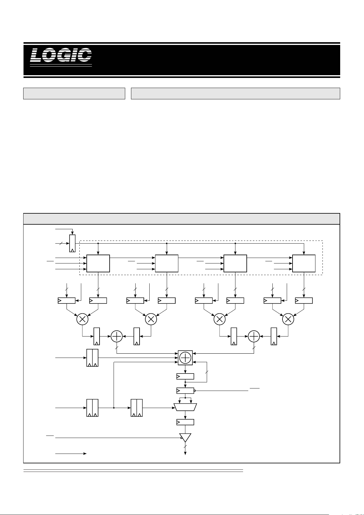
The LF2247 consists of an array of four
11 x 10-bit registered multipliers
followed by a summer and a 25-bit
accumulator. The LF2247 provides a
coefficient register file containing four
32 x 11-bit registers which are capable
of storing 32 different sets of filter
coefficients for the multiplier array.
All multiplier data inputs are user
accessible and can be updated every
clock cycle with either fractional or
integer two’s complement data. The
pipelined architecture has fully
registered input and output ports and
an asynchronous three-state output
enable control to simplify the design
of complex systems. The pipeline
latency for all inputs is five clock
cycles.
A 25-bit accumulator path allows
cumulative word growth which may
be internally rounded to 16 bits.
Output data is updated every clock
cycle and may be held under user
control. The data inputs/outputs and
control inputs are registered on the
rising edge of CLK. The Serial Data In
signal, SDIN, is registered on the
LF2247 BLOCK DIAGRAM
D1
9-0
10 11
ENB
1
D2
9-0
10 11
ENB
2
22
D3
9-0
10 11
ENB
3
D4
9-0
10 11
ENB
4
22
MS LS
S
15-0
ACC
FSEL
OEN
CLK TO ALL REGISTERS
(EXCEPT COEFFICIENT REGISTERS)
25
OCEN
Coefficient
Register 1
(32 x 11-bit)
Coefficient
Register 2
(32 x 11-bit)
Coefficient
Register 3
(32 x 11-bit)
Coefficient
Register 4
(32 x 11-bit)
A
4-0
SEN
SDIN
SCLK SCLK
5
ENBA
16
COEFFICIENT REGISTER FILE
SEN
SCLK
SEN
SCLK
SEN
DEVICES INCORPORATED
LF2247
Image Filter with Coefficient RAM
-2
Video Imaging Products
08/16/2000–LDS.2247-H
rising edge of SCLK. The LF2247
operates at a clock rate of 66 MHz
over the full temperature and supply
voltage ranges.
The LF2247 is applicable for performing pixel interpolation in image
manipulation and filtering applications. The LF2247 can perform a
bilinear interpolation of an image (4pixel kernels) at real-time video rates
when used with an image resampling
sequencer. Larger kernels or more
complex functions can be realized by
utilizing multiple devices.
Unrestricted access to all data ports
and an addressable coefficient register
file provides the LF2247 with considerable flexibility in applications such
as digital filters, adaptive FIR filters,
mixers, and other similar systems
requiring high-speed processing.
SIGNAL DEFINITIONS
Power
VCC and GND
+5 V power supply. All pins must be
connected.
Clocks
CLK — Master Clock
The rising edge of CLK strobes all
enabled registers except for the
coefficient registers.
SCLK — Serial Clock
The rising edge of SCLK shifts data
into and through the coefficient
register file when it is enabled for
serial data shifting.
Inputs
D19-0 – D49-0 — Data Input
D1–D4 are the 10-bit registered data
input ports. Data is latched on the
rising edge of CLK.
A4-0 — Row Address
A4-0 determines which row of data in
the coefficient register file is used to
feed data to the multiplier array. A4-0
is latched on the rising edge of CLK.
When a new row address is loaded
into the row address register, data
from the register file will be latched
into the multiplier input registers on
the next rising edge of CLK.
SDIN — Serial Data Input
SDIN is used to serially load data into
the coefficient registers. Data present
on SDIN is shifted into the coefficient
register file on the rising edge of SCLK
when SEN is LOW. The 11-bit coefficients are loaded into the coefficient
register file in 16-bit words as shown
in Figure 2. The five most significant
bits of the first 16-bit word determine
which row the data is written to in the
coefficient registers. Note that the five
most significant bits of the remaining
three 16-bit words are ignored. After
all four 16-bit words are shifted into
the register file, the lower eleven bits
of each word (the coefficient data) are
stored into the coefficient registers.
Outputs
S15-0 — Data Output
S15-0 is the 16-bit registered data
output port.
Controls
ENB1–ENB4 — Data Input Enables
The ENBN (N = 1, 2, 3, or 4) inputs
allow the DN registers to be updated
on each clock cycle. When ENBN is
LOW, data on DN9-0 is latched into
FIGURE 1B.OUTPUT FORMATS
15 14 13 10 9 81211 76543210
–2
6
(Sign)
252
4
21202
–1
232
2
2–22–32–42–52–62–72–82
–9
15 14 13 10 9 81211 76543210
–2
15
(Sign)
2142
13
210292
8
2122
11
272625242322212
0
Fractional Two's Complement (FSEL = 0)
Integer Two's Complement (FSEL = 1)
FIGURE 1A.INPUT FORMATS
987 210
–2
0
(Sign)
2–12
–2
2–72–82
–9
10 9 8 2 1 0
–2
1
(Sign)
202
–1
2–72–82
–9
987 210
–2
9
(Sign)
282
7
22212
0
10 9 8 2 1 0
–2
10
(Sign)
292
8
22212
0
Fractional Two's Complement (FSEL = 0)
Integer Two's Complement (FSEL = 1)
Data Coefficient

DEVICES INCORPORATED
Video Imaging Products
3
LF2247
Image Filter with Coefficient RAM
1
2
3
4
5
6
7
8
9
10
11
08/16/2000–LDS.2247-H
the DN register on the rising edge of
CLK. When ENBN is HIGH, data on
DN9-0 is not latched into the DN
register and the register contents will
not be changed.
ENBA — Row Address Input Enable
The ENBA input allows the row
address register to be updated on each
clock cycle. When ENBA is LOW,
data on A4-0 is latched into the row
address register on the rising edge of
CLK. When ENBA is HIGH, data on
A4-0 is not latched into the row
address register and the register
contents will not be changed.
OEN — Output Enable
When OEN is LOW, S15-0 is enabled
for output. When OEN is HIGH, S15-0
is placed in a high-impedance state.
OCEN — Clock Enable
When OCEN is LOW, data in the premux register (accumulator output) is
loaded into the output register on the
next rising edge of CLK. When OCEN
is HIGH, data in the pre-mux register
is held preventing the output
register’s contents from changing (if
FSEL does not change). Accumulation
continues internally as long as ACC is
HIGH, despite the state of OCEN.
FSEL — Format Select
When FSEL is LOW, the data input
during the current clock cycle is
assumed to be in fractional two’s
complement format, and the upper 16
bits of the accumulator are presented
at the output. Rounding of the
accumulator result to 16 bits is per-
formed if the accumulator control
input ACC is LOW. When FSEL is
HIGH, the data input is assumed to be
in integer two’s complement format,
and the lower 16 bits of the accumulator are presented at the output. No
rounding is performed when FSEL is
HIGH.
ACC — Accumulator Control
The ACC input determines whether
internal accumulation is performed on
the data input during the current
clock cycle. If ACC is LOW, no
accumulation is performed, the prior
accumulated sum is cleared, and the
current sum of products is output. If
FSEL is also LOW, one-half LSB
rounding to 16 bits is performed on
the result. When ACC is HIGH, the
emerging product is added to the sum
of the previous products, without
additional rounding.
SEN — Serial Input Enable
The SEN input enables the shifting of
serial data through the registers in the
coefficient register file. When SEN is
LOW, serial data on SDIN is shifted
into the coefficient register file on the
rising edge of SCLK. SEN must
remain LOW until all four coefficients
have been clocked in. SEN does not
need to be pulsed between consecutive data sets. It can remain LOW
while the entire register file is loaded
by a constant bit stream. When SEN is
HIGH, data can not be shifted into the
register file and the register file’s
contents will not be changed. When
enabling the coefficient register file for
serial data input, the LF2247 requires
a HIGH to LOW transition of SEN in
order to function properly. Therefore,
SEN needs to be set HIGH immediately after power up to ensure proper
operation of the serial input circuitry.
FIGURE 2. SERIAL DATA FORMAT
231564897111210 13 15 1614 18 1917 21 2220 24 2523 27 2826 29 31 3230
34 3533 37 3836 40 4139 43 4442 45 47 4846 50 5149 53 5452 56 5755 59 6058 61 63 6462
0000111111011001XXXX0X0100001001
XXXX0X1101000001XXXX1X1111010001
FIRST 16-BIT WORD SECOND 16-BIT WORD
THIRD 16-BIT WORD FOURTH 16-BIT WORD
ROW
ADDRESS
DATA FOR
COEFFICIENT REGISTER 4
DON'T
CARES
DATA FOR
COEFFICIENT REGISTER 3
DON'T
CARES
DATA FOR
COEFFICIENT REGISTER 2
DON'T
CARES
DATA FOR
COEFFICIENT REGISTER 1
SHOWN IS SERIAL DATA STREAM TO LOAD ROW ADDRESS 2 WITH:
COEFFICIENT REGISTER 1 = 7E4
COEFFICIENT REGISTER 2 = 1A4
COEFFICIENT REGISTER 3 = 08C
COEFFICIENT REGISTER 4 = 7EC

DEVICES INCORPORATED
LF2247
Image Filter with Coefficient RAM
-4
Video Imaging Products
08/16/2000–LDS.2247-H
Storage temperature ........................................................................................................... –65°C to +150°C
Operating ambient temperature........................................................................................... –55°C to +125°C
VCC supply voltage with respect to ground............................................................................ –0.5 V to +7.0V
Input signal with respect to ground ............................................................................... –0.5 V to VCC + 0.5 V
Signal applied to high impedance output ...................................................................... –0.5 V to VCC + 0.5 V
Output current into low outputs............................................................................................................. 25 mA
Latchup current ............................................................................................................................... > 400 mA
MAXIMUM RATINGS
Above which useful life may be impaired (Notes 1, 2, 3, 8)
Symbol Parameter Test Condition Min Typ Max Unit
VOH Output High Voltage VCC = Min., IOH = –2.0 mA 2.4 V
VOL Output Low Voltage VCC = Min., IOL = 4.0 mA 0.4 V
VIH Input High Voltage 2.0 VCC V
V IL Input Low Voltage (Note 3) 0.0 0.8 V
IIX Input Current Ground ≤ VIN ≤ VCC (Note 12) ±10 µA
IOZ Output Leakage Current Ground ≤ VOUT ≤ VCC (Note 12) ±40 µA
ICC1 VCC Current, Dynamic (Notes 5, 6) 100 mA
ICC2 VCC Current, Quiescent (Note 7) 6.0 mA
CIN Input Capacitance TA = 25°C, f = 1 MHz 10 pF
COUT Output Capacitance TA = 25°C, f = 1 MHz 10 pF
ELECTRICAL CHARACTERISTICS
Over Operating Conditions (Note 4)
OPERATING CONDITIONS
To meet specified electrical and switching characteristics
Mode Temperature Range (Ambient) Supply Voltage
Active Operation, Commercial 0°C to +70°C 4.75 V ≤ VCC ≤ 5.25 V
Active Operation, Military –55°C to +125°C 4.50 V ≤ VCC ≤ 5.50 V

DEVICES INCORPORATED
Video Imaging Products
5
LF2247
Image Filter with Coefficient RAM
1
2
3
4
5
6
7
8
9
10
11
08/16/2000–LDS.2247-H
1234567890123456
1
23456789012345
6
1
23456789012345
6
1
23456789012345
6
1
23456789012345
6
1
23456789012345
6
1
23456789012345
6
1
23456789012345
6
1
23456789012345
6
1
23456789012345
6
1
23456789012345
6
1
23456789012345
6
1
23456789012345
6
1
23456789012345
6
1
23456789012345
6
1
23456789012345
6
1
23456789012345
6
1
23456789012345
6
1
23456789012345
6
1
23456789012345
6
1
23456789012345
6
1
23456789012345
6
1
23456789012345
6
1
23456789012345
6
1
23456789012345
6
1
23456789012345
6
1
23456789012345
6
1
23456789012345
6
1
23456789012345
6
1
23456789012345
6
1
23456789012345
6
1234567890123456
23456789012345678901234567890
1
23456789012345678901234567890
1
23456789012345678901234567890
1
23456789012345678901234567890
1
23456789012345678901234567890
1
23456789012345678901234567890
1
23456789012345678901234567890
1
23456789012345678901234567890
1
23456789012345678901234567890
1
23456789012345678901234567890
1
23456789012345678901234567890
1
23456789012345678901234567890
1
23456789012345678901234567890
1
23456789012345678901234567890
1
23456789012345678901234567890
1
23456789012345678901234567890
1
23456789012345678901234567890
1
23456789012345678901234567890
1
23456789012345678901234567890
1
23456789012345678901234567890
1
23456789012345678901234567890
1
23456789012345678901234567890
1
23456789012345678901234567890
1
23456789012345678901234567890
1
23456789012345678901234567890
1
23456789012345678901234567890
1
23456789012345678901234567890
1
23456789012345678901234567890
1
23456789012345678901234567890
1
23456789012345678901234567890
1
SWITCHING CHARACTERISTICS
LF2247–
33
*
25 15
Symbol Parameter Min Max Min Max Min Max
tCYC Cycle Time 33 25 15
tPWL Clock Pulse Width Low 15 10 7
tPWH Clock Pulse Width High 10 10 7
tS Input Setup Time 10 8 5
tH Input Hold Time 0 0 0
tD Output Delay 15 13 11
tDIS Three-State Output Disable Delay (Note 11) 15 15 15
tENA Three-State Output Enable Delay (Note 11) 15 15 15
COMMERCIAL OPERATING RANGE (0°C to +70°C)
Notes 9, 10 (ns)
LF2247–
33
*
25
*
Symbol Parameter Min Max Min Max
tCYC Cycle Time 33 25
tPWL Clock Pulse Width Low 15 10
tPWH Clock Pulse Width High 10 10
tS Input Setup Time 10 8
tH Input Hold Time 0 0
tD Output Delay 15 13
tDIS Three-State Output Disable Delay (Note 11) 15 15
tENA Three-State Output Enable Delay (Note 11) 15 15
MILITARY OPERATING RANGE (–55°C to +125°C)
Notes 9, 10 (ns)
2345678901234567890123
4
*DISCONTINUED SPEED GRADE
SWITCHING WAVEFORMS:DATA I/O
CLK
D1
9-0
– D4
9-0
CONTROLS
t
PWH
t
PWL
t
CYC
A
4-0
(Except OEN)
OEN
S
15-0
123456
t
H
t
S
D
N
D
N+1
A
N+1
A
N+2
t
D
t
DIS
HIGH IMPEDANCE
t
ENA
S
N
S
N–1
S
N+1

DEVICES INCORPORATED
LF2247
Image Filter with Coefficient RAM
-6
Video Imaging Products
08/16/2000–LDS.2247-H
23456789012345678901234567890
1
23456789012345678901234567890
1
23456789012345678901234567890
1
23456789012345678901234567890
1
23456789012345678901234567890
1
23456789012345678901234567890
1
23456789012345678901234567890
1
23456789012345678901234567890
1
23456789012345678901234567890
1
23456789012345678901234567890
1
23456789012345678901234567890
1
23456789012345678901234567890
1
23456789012345678901234567890
1
23456789012345678901234567890
1
23456789012345678901234567890
1
23456789012345678901234567890
1
23456789012345678901234567890
1
23456789012345678901234567890
1
23456789012345678901234567890
1
23456789012345678901234567890
1
23456789012345678901234567890
1
23456789012345678901234567890
1
23456789012345678901234567890
1
23456789012345678901234567890
1
23456789012345678901234567890
1
23456789012345678901234567890
1
1234567890123456
1
23456789012345
6
1
23456789012345
6
1
23456789012345
6
1
23456789012345
6
1
23456789012345
6
1
23456789012345
6
1
23456789012345
6
1
23456789012345
6
1
23456789012345
6
1
23456789012345
6
1
23456789012345
6
1
23456789012345
6
1
23456789012345
6
1
23456789012345
6
1
23456789012345
6
1
23456789012345
6
1
23456789012345
6
1
23456789012345
6
1
23456789012345
6
1
23456789012345
6
1
23456789012345
6
1
23456789012345
6
1
23456789012345
6
1
23456789012345
6
1
23456789012345
6
1
23456789012345
6
1
23456789012345
6
1234567890123456
LF2247–
33
*
25 15
Symbol Parameter Min Max Min Max Min Max
tSCYC Serial Interface Cycle Time 62 62 62
tSWL Serial Clock Pulse Width Low 30 30 30
tSWH Serial Clock Pulse Width High 30 30 30
tSENS Serial Enable Setup Time 20 20 20
tSENH Serial Enable Hold Time 0 0 0
tSS Serial Data Input Setup Time 20 20 20
tSH Serial Data Input Hold Time 0 0 0
SWITCHING CHARACTERISTICS
COMMERCIAL OPERATING RANGE (0°C to +70°C)
Notes 9, 10 (ns)
LF2247–
33
*
25
*
Symbol Parameter Min Max Min Max
tSCYC Serial Interface Cycle Time 62 62
tSWL Serial Clock Pulse Width Low 30 30
tSWH Serial Clock Pulse Width High 30 30
tSENS Serial Enable Setup Time 20 20
tSENH Serial Enable Hold Time 0 0
tSS Serial Data Input Setup Time 20 20
tSH Serial Data Input Hold Time 0 0
MILITARY OPERATING RANGE (–55°C to +125°C)
Notes 9, 10 (ns)
2345678901234567890123
4
*DISCONTINUED SPEED GRADE
SWITCHING WAVEFORMS:SERIAL DATA INPUT
SCLK
t
SWH
t
SWL
t
SCYC
t
SENS
t
SS
t
SH
A
4
A
3
C1
1
C1
0
t
SENH
SEN
SDIN
1 2 63 64

DEVICES INCORPORATED
Video Imaging Products
7
LF2247
Image Filter with Coefficient RAM
1
2
3
4
5
6
7
8
9
10
11
08/16/2000–LDS.2247-H
1. Maximum Ratings indicate stress
specifications only. Functional operation of these products at values beyond
those indicated in the Operating Conditions table is not implied. Exposure to
maximum rating conditions for extended periods may affect reliability.
2. The products described by this specification include internal circuitry designed to protect the chip from damaging substrate injection currents and accumulations of static charge. Nevertheless, conventional precautions should
be observed during storage, handling,
and use of these circuits in order to
avoid exposure to excessive electrical
stress values.
3. This device provides hard clamping of
transient undershoot and overshoot. Input levels below ground or above VCC
will be clamped beginning at –0.6 V and
VCC + 0.6 V. The device can withstand
indefinite operation with inputs in the
range of –0.5 V to +7.0 V. Device operation will not be adversely affected, however, input current levels will be well in
excess of 100 mA.
4. Actual test conditions may vary from
those designated but operation is guaranteed as specified.
5. Supply current for a given application can be accurately approximated by:
where
N = total number of device outputs
C = capacitive load per output
V = supply voltage
F = clock frequency
6. Tested with all outputs changing every cycle and no load, at a 30 MHz clock
rate.
7. Tested with all inputs within 0.1 V of
VCC or Ground, no load.
8. These parameters are guaranteed
but not 100% tested.
NCV F
4
2
NOTES
9. AC specifications are tested with
input transition times less than 3 ns,
output reference levels of 1.5 V (except
tDIS test), and input levels of nominally
0 to 3.0 V. Output loading may be a
resistive divider which provides for
specified IOH and IOL at an output
voltage of VOH min and VOL max
respectively. Alternatively, a diode
bridge with upper and lower current
sources of IOH and IOL respectively,
and a balancing voltage of 1.5 V may be
used. Parasitic capacitance is 30 pF
minimum, and may be distributed.
This device has high-speed outputs capable of large instantaneous current
pulses and fast turn-on/turn-off times.
As a result, care must be exercised in the
testing of this device. The following
measures are recommended:
a. A 0.1 µF ceramic capacitor should be
installed between VCC and Ground
leads as close to the Device Under Test
(DUT) as possible. Similar capacitors
should be installed between device VCC
and the tester common, and device
ground and tester common.
b. Ground and VCC supply planes
must be brought directly to the DUT
socket or contactor fingers.
c. Input voltages should be adjusted to
compensate for inductive ground and VCC
noise to maintain required DUT input
levels relative to the DUT ground pin.
10. Each parameter is shown as a minimum or maximum value. Input requirements are specified from the point
of view of the external system driving
the chip. Setup time, for example, is
specified as a minimum since the external system must supply at least that
much time to meet the worst-case requirements of all parts. Responses from
the internal circuitry are specified from
the point of view of the device. Output
delay, for example, is specified as a
maximum since worst-case operation of
any device always provides data within
that time.
11. For the tENA test, the transition is
measured to the 1.5 V crossing point
with datasheet loads. For the tDIS test,
the transition is measured to the
±200mV level from the measured
steady-state output voltage with
±10mA loads. The balancing voltage, VTH, is set at 3.5 V for Z-to-0
and 0-to-Z tests, and set at 0 V for Zto-1 and 1-to-Z tests.
12. These parameters are only tested at
the high temperature extreme, which is
the worst case for leakage current.
S1
I
OH
I
OL
V
TH
C
L
DUT
OE
0.2 V
t
DIS
t
ENA
0.2 V
1.5 V 1.5 V
3.5V Vth
1
Z
0
Z
Z
1
Z
0
1.5 V
1.5 V
0V Vth
VOL*
V
OH
*
V
OL
*
V
OH
*
Measured V
OL
with IOH = –10mA and IOL = 10mA
Measured V
OH
with IOH = –10mA and IOL = 10mA
FIGURE B. THRESHOLD LEVELS
FIGURE A. OUTPUT LOADING CIRCUIT

DEVICES INCORPORATED
LF2247
Image Filter with Coefficient RAM
-8
Video Imaging Products
08/16/2000–LDS.2247-H
0°C to +70°C — COMMERCIAL SCREENING
ORDERING INFORMATION
84-pin
1234567
74
73
72
71
70
69
68
67
66
65
64
63
62
61
60
59
58
57
56
55
54
84 83 82 81 80 79
4443 45 46 47 493837 39 40 41 42
12
13
14
15
16
17
18
19
20
21
22
23
24
25
26
27
28
29
30
31
32
48
Top
View
891011 78 77 76 75
36353433 50 51 52 53
D1
5
D1
4
D1
3
D1
2
D1
1
D1
0
D1
9
D1
8
D1
7
D1
6
GND
SDIN
V
CC
SCLK
SEN
A
0
A
1
A
2
A
3
A
4
ENBA
CLK
ENB
1
ENB
2
ENB
3
D4
9
D4
8
D4
7
D4
6
D4
5
D4
4
D4
3
D4
2
D4
1
GND
D4
0
ENB
4
GND
OEN
OCEN
ACC
FSEL
D20D21D22D23D24D25D26D27D28D29D3
9
GND
D3
8D37D36D35D34D33D32D31D30
S0S1GND
S2S3S4VCCS5S6S7GND
S8S9S10VCCS11S12S13GND
S14S
15
Plastic J-Lead Chip Carrier
(J3)
LF2247JC15
Speed
15 ns

DEVICES INCORPORATED
Video Imaging Products
9
LF2247
Image Filter with Coefficient RAM
1
2
3
4
5
6
7
8
9
10
11
08/16/2000–LDS.2247-H
0°C to +70°C — COMMERCIAL SCREENING
ORDERING INFORMATION
100-pin
Plastic Quad Flatpack
(Q2)
LF2247QC25
LF2247QC15
Speed
25 ns
15 ns
S0
NC
D1
5
D14
D13
D12
D11
D10
D19
D18
D17
D16
GND
GND
NC
SDIN
NC
V
CC
VCC
SCLK
SEN
A
0
A1
A2
A3
A4
ENBA
NC
NC
D2
0
S1
GND
GND
S2S3S4VCCS5S6S7GND
S8S9
S10
VCC
S11
S12
S13
GND
S
14
S15
CLK
NC
ENB
1
ENB2
ENB3
D49
D48
D47
D46
D45
D44
D43
D42
D41
GND
GND
D4
0
ENB4
NC
GND
GND
OEN
OCEN
ACC
FSEL
NC
NC
NC
NC
D21
D22
D23
D24
D25
D26
D27
D28
D29
D39
GND
D3
8
D37
D36
D35
D34
D33
D32
D31
D30
80
79
78
77
76
75
74
73
72
71
70
69
68
67
66
65
64
63
62
61
60
59
58
57
56
55
54
53
52
51
Top
View
1
2
3
4
5
6
7
8
9
10
11
12
13
14
15
16
17
18
19
20
21
22
23
24
25
26
27
28
29
30
31323334353637383940414243444546474849
50
100
99989796959493929190898887868584838281

DEVICES INCORPORATED
LF2247
Image Filter with Coefficient RAM
-10
Video Imaging Products
08/16/2000–LDS.2247-H
23456789012345678901234567890121234567890123456789012345678901212345678901234567890123456789012
1
23456789012345678901234567890121234567890123456789012345678901212345678901234567890123456789012
1
23456789012345678901234567890121234567890123456789012345678901212345678901234567890123456789012
1
23456789012345678901234567890121234567890123456789012345678901212345678901234567890123456789012
1
23456789012345678901234567890121234567890123456789012345678901212345678901234567890123456789012
1
23456789012345678901234567890121234567890123456789012345678901212345678901234567890123456789012
1
23456789012345678901234567890121234567890123456789012345678901212345678901234567890123456789012
1
23456789012345678901234567890121234567890123456789012345678901212345678901234567890123456789012
1
23456789012345678901234567890121234567890123456789012345678901212345678901234567890123456789012
1
23456789012345678901234567890121234567890123456789012345678901212345678901234567890123456789012
1
23456789012345678901234567890121234567890123456789012345678901212345678901234567890123456789012
1
23456789012345678901234567890121234567890123456789012345678901212345678901234567890123456789012
1
23456789012345678901234567890121234567890123456789012345678901212345678901234567890123456789012
1
23456789012345678901234567890121234567890123456789012345678901212345678901234567890123456789012
1
23456789012345678901234567890121234567890123456789012345678901212345678901234567890123456789012
1
23456789012345678901234567890121234567890123456789012345678901212345678901234567890123456789012
1
23456789012345678901234567890121234567890123456789012345678901212345678901234567890123456789012
1
23456789012345678901234567890121234567890123456789012345678901212345678901234567890123456789012
1
23456789012345678901234567890121234567890123456789012345678901212345678901234567890123456789012
1
23456789012345678901234567890121234567890123456789012345678901212345678901234567890123456789012
1
23456789012345678901234567890121234567890123456789012345678901212345678901234567890123456789012
1
23456789012345678901234567890121234567890123456789012345678901212345678901234567890123456789012
1
23456789012345678901234567890121234567890123456789012345678901212345678901234567890123456789012
1
23456789012345678901234567890121234567890123456789012345678901212345678901234567890123456789012
1
23456789012345678901234567890121234567890123456789012345678901212345678901234567890123456789012
1
23456789012345678901234567890121234567890123456789012345678901212345678901234567890123456789012
1
23456789012345678901234567890121234567890123456789012345678901212345678901234567890123456789012
1
23456789012345678901234567890121234567890123456789012345678901212345678901234567890123456789012
1
23456789012345678901234567890121234567890123456789012345678901212345678901234567890123456789012
1
23456789012345678901234567890121234567890123456789012345678901212345678901234567890123456789012
1
23456789012345678901234567890121234567890123456789012345678901212345678901234567890123456789012
1
23456789012345678901234567890121234567890123456789012345678901212345678901234567890123456789012
1
23456789012345678901234567890121234567890123456789012345678901212345678901234567890123456789012
1
23456789012345678901234567890121234567890123456789012345678901212345678901234567890123456789012
1
23456789012345678901234567890121234567890123456789012345678901212345678901234567890123456789012
1
23456789012345678901234567890121234567890123456789012345678901212345678901234567890123456789012
1
23456789012345678901234567890121234567890123456789012345678901212345678901234567890123456789012
1
23456789012345678901234567890121234567890123456789012345678901212345678901234567890123456789012
1
23456789012345678901234567890121234567890123456789012345678901212345678901234567890123456789012
1
23456789012345678901234567890121234567890123456789012345678901212345678901234567890123456789012
1
23456789012345678901234567890121234567890123456789012345678901212345678901234567890123456789012
1
23456789012345678901234567890121234567890123456789012345678901212345678901234567890123456789012
1
23456789012345678901234567890121234567890123456789012345678901212345678901234567890123456789012
1
23456789012345678901234567890121234567890123456789012345678901212345678901234567890123456789012
1
23456789012345678901234567890121234567890123456789012345678901212345678901234567890123456789012
1
23456789012345678901234567890121234567890123456789012345678901212345678901234567890123456789012
1
23456789012345678901234567890121234567890123456789012345678901212345678901234567890123456789012
1
23456789012345678901234567890121234567890123456789012345678901212345678901234567890123456789012
1
23456789012345678901234567890121234567890123456789012345678901212345678901234567890123456789012
1
23456789012345678901234567890121234567890123456789012345678901212345678901234567890123456789012
1
23456789012345678901234567890121234567890123456789012345678901212345678901234567890123456789012
1
23456789012345678901234567890121234567890123456789012345678901212345678901234567890123456789012
1
23456789012345678901234567890121234567890123456789012345678901212345678901234567890123456789012
1
23456789012345678901234567890121234567890123456789012345678901212345678901234567890123456789012
1
23456789012345678901234567890121234567890123456789012345678901212345678901234567890123456789012
1
23456789012345678901234567890121234567890123456789012345678901212345678901234567890123456789012
1
23456789012345678901234567890121234567890123456789012345678901212345678901234567890123456789012
1
23456789012345678901234567890121234567890123456789012345678901212345678901234567890123456789012
1
23456789012345678901234567890121234567890123456789012345678901212345678901234567890123456789012
1
23456789012345678901234567890121234567890123456789012345678901212345678901234567890123456789012
1
23456789012345678901234567890121234567890123456789012345678901212345678901234567890123456789012
1
23456789012345678901234567890121234567890123456789012345678901212345678901234567890123456789012
1
23456789012345678901234567890121234567890123456789012345678901212345678901234567890123456789012
1
23456789012345678901234567890121234567890123456789012345678901212345678901234567890123456789012
1
23456789012345678901234567890121234567890123456789012345678901212345678901234567890123456789012
1
23456789012345678901234567890121234567890123456789012345678901212345678901234567890123456789012
1
23456789012345678901234567890121234567890123456789012345678901212345678901234567890123456789012
1
ORDERING INFORMATION
84-pin
A
B
C
D
E
F
G
H
J
K
L
Top View
Through Package
(i.e., Component Side Pinout)
12345
6
7 8 9 10 11
D4
9
ENB
1
CLK
GND
S
11
S
10
S
7
V
CC
S
2
S
1
D1
5
D4
8
ENB
3
S
12
S
9
S
8
S
0
D1
4
D4
6
D4
7
D1
3
D1
2
D4
3
D4
4
D4
5
D1
1
D1
0
D1
9
D4
2
GND
D4
1
D1
7
D1
8
V
CC
D4
0
ENB
4
GND
D1
6
SDIN
GND
OEN
OCEN
SEN
SCLK
ENB
2
S
15
S
14
S
13
V
CC
S
6
GND
S
5
S
4
S
3
GND
ACC
D3
0
D3
8
D2
8
D2
7
A
2
A
0
FSEL
D3
1
D3
3
D3
6
GND
D2
4
D2
5
D2
2
ENBA
A
4
A
1
D3
2
D3
4
D3
5
D3
7
D3
9
D2
9
D2
6
D2
3
D2
1
D2
0
A
3
Ceramic Pin Grid Array
(G3)
Speed
–55°C to +125°C — COMMERCIAL SCREENING
–55°C to +125°C — MIL-STD-883 COMPLIANT
0°C to +70°C — COMMERCIAL SCREENING
Discontinued Package
 Loading...