

DEVICES INCORPORATED
12/16-bit Half-Band Interpolating/
DEVICES INCORPORATED
FEATURES DESCRIPTION
LF2242
12/16-bit Half-Band Interpolating/
LF2242
Decimating Digital Filter
Decimating Digital Filter
❑❑
❑ 40 MHz Clock Rate
❑❑
❑❑
❑ Passband (0 to 0.22f
❑❑
)
S
Ripple: ±0.02 dB
❑❑
❑ Stopband (0.28f
❑❑
to 0.5fS)
S
Rejection: 59.4 dB
❑❑
❑ User-Selectable 2:1 Decimation or
❑❑
1:2 Interpolation
❑❑
❑ 12-bit Two’s Complement Input
❑❑
and 16-bit Output with
User-Selectable Rounding, 8- to
16-Bits
❑❑
❑ User-Selectable Two’s Complement
❑❑
or Inverted Offset Binary Output
Formats
❑❑
❑ Three-State Outputs
❑❑
❑❑
❑ Replaces TRW/ Raytheon/
❑❑
Fairchild TMC2242
❑❑
❑ Package Styles Available:
❑❑
• 44-pin PLCC, J-Lead
• 44-pin PQFP
The LF2242 is a linear-phase, half-
band (low pass) interpolating/
decimating digital filter that, unlike
intricate analog filters, requires no
tuning. The LF2242 can also significantly reduce the complexity of
traditional analog anti-aliasing prefilters without compromising the
signal bandwidth or attenuation. This
can be achieved by using the LF2242
as a decimating post-filter with an
A/D converter and by sampling the
signal at twice the rate needed.
Likewise, by using the LF2242 as an
interpolating pre-filter with a D/A
converter, the corresponding analog
reconstruction post-filter circuitry can
be simplified.
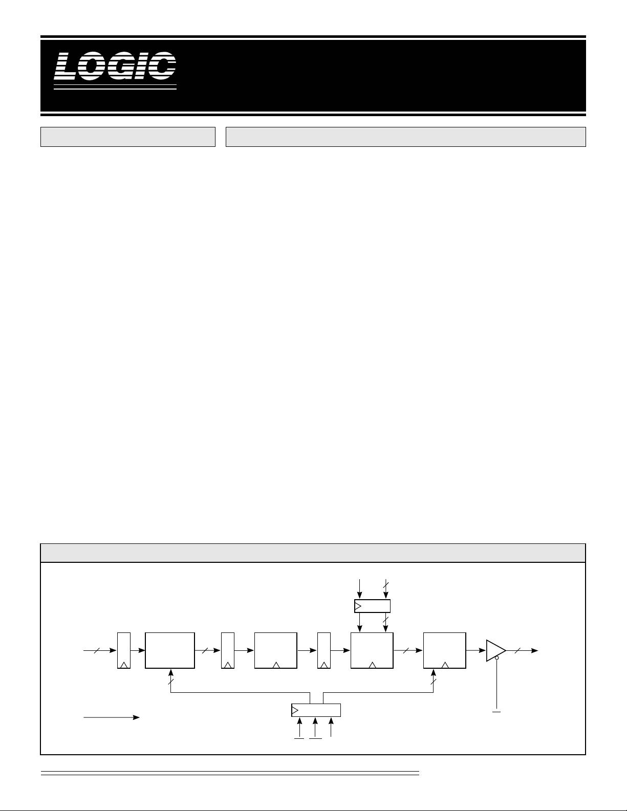
The coefficients of the LF2242 are
fixed, and the only user programming
required is the selection of the mode
(interpolate, decimate, or passthrough) and rounding. The asynchronous three-state output enable
control simplifies interfacing to a bus.
Data can be input into the LF2242 at a
rate of up to 40 million samples per
second. Within the 40 MHz I/O limit,
the output sample rate can be onehalf, equal to, or two times the input
sample rate. Once data is clocked in,
the 55-value output response begins
after 7 clock cycles and ends after 61
clock cycles. The pipeline latency
from the input of an impulse response
to its corresponding output peak is 34
clock cycles.
The output data may be in either
two’s complement format or inverted
offset binary format. To avoid
truncation errors, the output data is
always internally rounded before it is
latched into the output register.
Rounding is user-selectable, and the
output data can be rounded from 16
bit values down to 8 bit values.
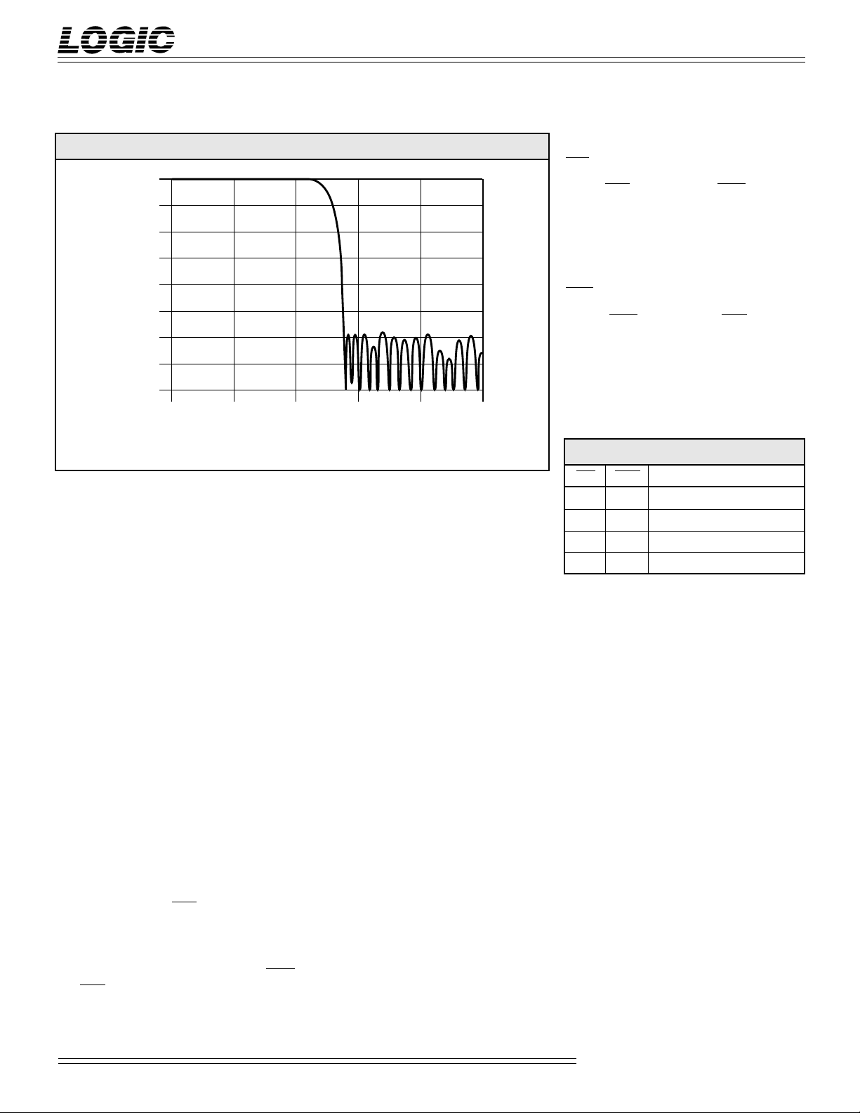
DC gain of the LF2242 is 1.0015
(0.0126 dB) in pass-through and
decimate modes and 0.5007 (–3.004
dB) in interpolate mode. Passband
ripple does not exceed ±0.02 dB from
0 to 0.22fS with stopband attenuation
greater than 59.4 dB from 0.28fS to
0.5fS (Nyquist frequency). The
response of the filter is –6 dB at 0.25fS.
Full compliance with CCIR Recommendation 601 (–12 dB at 0.25fS) can
be achieved by cascading two devices
serially.
LF2242 BLOCK DIAGRAM
SI
11–0
CLK
INTERPOLATION
CIRCUIT
3
TO ALL REGISTERS
55-TAP
FIR
FILTER
RND
3
3
ROUND
CIRCUIT
2–0
161212
DECIMATION
CIRCUIT
3
OE
16
SO
15–0
TCO
AND LIMIT
SYNCINT DEC
Video Imaging Products
1
08/16/2000–LDS.2242-K
DEVICES INCORPORATED
LF2242
12/16-bit Half-Band Interpolating/
Decimating Digital Filter
FIGURE 1. FREQUENCY RESPONSE OF FILTER
0
–10
–20
–30
–40
–50
GAIN (dB)
–60
–70
–80
0 0.1
SIGNAL DEFINITIONS
Power
VCC and GND
+5 V power supply. All pins must be
connected.
ƒ
0.2
S
ƒ
S
FREQUENCY (NORMALIZED)
Inputs
SI11–0 — Data Input
12-bit two’s complement data input
port. Data is latched into the register on
the rising edge of CLK. The LSB is SI0
(Figure 2).
0.3
Controls
INT — Interpolation Control
When INT is LOW and DEC is HIGH
(Table 1), the device internally forces
every other incoming data sample to
zero. This effectively halves the input
data rate and the output amplitude.
DEC — Decimation Control
When DEC is LOW and INT is HIGH
(Table 1), the output register is strobed on
every other rising edge of CLK (driven at
half the clock rate), decimating the output
data stream.
ƒ
0.4
S
ƒ
0.5
S
ƒ
S
TABLE 1. MODE SELECTION
INT DEC MODE
0 0 Pass-through*
0 1 Interpolate
1 0 Decimate
1 1 Pass-through*
*Input and output registers run at full
clock rate
Clock
CLK — Master Clock
The rising edge of CLK strobes all registers. All timing specifications are referenced to the rising edge of CLK.
SYNC — Synchronization Control
Incoming data is synchronized by holding SYNC HIGH on CLKN, and then by
bringing SYNC LOW on CLKN+1 with
the first word of input data. SYNC is held
LOW until resynchronization is desired,
or it can be toggled at half the clock rate.
For interpolation (INT = LOW), input
data should be presented at the first rising edge of CLK for which SYNC is LOW
and then at every alternate rising edge of
CLK thereafter. SYNC is inactive if DEC
and INT are equal (pass-through mode).
Outputs
SO15-0 Data Output
The current 16-bit result is available on
the SO15-0 outputs. The LF2242’s limiter
ensures that a valid full-scale (7FFF
positive or 8000 negative) output will be
generated in the event of an internal
overflow. The LSB is SO0 (Figure 2).
2
Video Imaging Products
08/16/2000–LDS.2242-K
DEVICES INCORPORATED
LF2242
12/16-bit Half-Band Interpolating/
Decimating Digital Filter
FIGURE 2. INPUT AND OUTPUT FORMATS
Two’s Complement Input Format
10 9 8 2 1 011 3
02–12–2
–2
(Sign)
–3
2
2–82–92
Two’s Complement Output Format (TCO = 1, Non-interpolate)
14 13 12 2 1 015 3
02–12–2
–2
(Sign)
–3
2
–122–132–14
2
Two’s Complement Output Format (TCO = 1, Interpolate)
14 13 12 2 1 015 3
1202–1
–2
(Sign)
–2
2
–112–122–13
2
Inverted Offset Binary Output Format (TCO = 0, Non-interpolate)
14 13 12 2 1 015 3
02–12–2
2
(Sign)
–3
2
–122–132–14
2
Inverted Offset Binary Output Format (TCO = 0, Interpolate)
14 13 12 2 1 015 3
1202–1
2
(Sign)
–2
2
–112–122–13
2
–10
–11
2
–15
2
–14
2
–15
2
–14
2
RND2-0 — Rounding Control
The rounding control inputs set the position of the effective LSB of the output data
by adding a rounding bit to the internal
bit position that is one below that specified by RND2-0. All bits below the effective LSB position are subsequently zeroed (Table 2).
TCO — Two’s Complement Format
Control
The TCO input determines the format of
the output data. When TCO is HIGH, the
output data is presented in two’s complement format. When TCO is LOW, the
data is in inverted offset binary format
(all output bits are inverted except the
MSB — the MSB is unchanged).
OE — Output Enable
When the OE signal is LOW, the current
data in the output register is available on
the SO15-0 pins. When OE is HIGH, the
outputs are in a high-impedance state.
TABLE 2. ROUNDING FORMAT
RND2-0 SO15 SO14 SO13 SO12 • • • SO8 SO7 SO6 SO5 SO4 SO3 SO2 SO1 SO0
000XXXX• • • XXXXXXXXR
001XXXX• • • XXXXXXXR0
010XXXX• • • XXXXXXR00
011XXXX• • • XXXXXR000
100XXXX• • • XXXXR0000
101XXXX
• • • XXXR00000
110XXXX• • • XXR000000
111XXXX• • • XR0000000
'R' indicates the half-LSB rounded bit (effective LSB position)
Video Imaging Products
3
08/16/2000–LDS.2242-K

DEVICES INCORPORATED
LF2242
12/16-bit Half-Band Interpolating/
Decimating Digital Filter
MAXIMUM RATINGS
Storage temperature ........................................................................................................... –65°C to +150°C
Operating ambient temperature........................................................................................... –55°C to +125°C
VCC supply voltage with respect to ground............................................................................ –0.5 V to +7.0V
Input signal with respect to ground ............................................................................... –0.5 V to VCC + 0.5 V
Signal applied to high impedance output ...................................................................... –0.5 V to VCC + 0.5 V
Output current into low outputs............................................................................................................. 25 mA
Latchup current ............................................................................................................................... > 400 mA
OPERATING CONDITIONS
Active Operation, Commercial 0°C to +70°C 4.75 V ≤ VCC ≤ 5.25V
Active Operation, Industrial -40°C to +85°C 4.75 V ≤ VCC ≤ 5.25V
ELECTRICAL CHARACTERISTICS
Above which useful life may be impaired (Notes 1, 2, 3, 8)
To meet specified electrical and switching characteristics
Mode Temperature Range (Ambient) Supply Voltage
Over Operating Conditions (Note 4)
Symbol Parameter Test Condition Min Typ Max Unit
VOH Output High Voltage VCC = Min., IOH = –2.0 mA 2.4 V
VOL Output Low Voltage VCC = Min., IOL = 4.0 mA 0.4 V
VIH Input High Voltage 2.0 VCC V
V IL Input Low Voltage (Note 3) 0.0 0.8 V
IIX Input Current Ground ≤ VIN ≤ VCC (Note 12) ±10 µA
IOZ Output Leakage Current (Note 12) ±10 µA
ICC1 VCC Current, Dynamic (Notes 5, 6) 80 mA
ICC2 VCC Current, Quiescent (Note 7) 10 mA
CIN Input Capacitance TA = 25°C, f = 1 MHz 10 pF
COUT Output Capacitance TA = 25°C, f = 1 MHz 10 pF
Video Imaging Products
4
08/16/2000–LDS.2242-K

DEVICES INCORPORATED
SWITCHING CHARACTERISTICS
LF2242
12/16-bit Half-Band Interpolating/
Decimating Digital Filter
COMMERCIAL OPERATING RANGE (0°C to +70°C)
Notes 9, 10 (ns)
LF2242–
33 25
Symbol Parameter Min Max Min Max
tCYC Cycle Time 33 25
tPW Clock Pulse Width 10 10
tS Input Setup Time 10 8
tH Input Hold Time 0 0
tD Output Delay 20 16
tDIS Three-State Output Disable Delay (Note 11) 15 15
tENA Three-State Output Enable Delay (Note 11) 15 15
SWITCHING WAVEFORMS:PASS-THROUGH MODE (INT = DEC)
CLK
SYNC
SI
SO
11-0
15-0
123 7
t
t
PW
t
H
N
t
S
N+1 N+2
PW
t
D
HIGH IMPEDANCE
t
DIS
t
ENA
f(N)f(
8910
N+1
)f(
N+2
)
OE
Video Imaging Products
5
08/16/2000–LDS.2242-K

DEVICES INCORPORATED
SWITCHING WAVEFORMS:INTERPOLATE MODE (INT = 0, DEC = 1)
LF2242
12/16-bit Half-Band Interpolating/
Decimating Digital Filter
123 7
CLK
tS
tPW
tPW
SYNC
SI11-0
SO15-0
N
tH
N+2
tDIS
tD
HIGH IMPEDANCE
tENA
OE
SWITCHING WAVEFORMS:DECIMATE MODE (INT = 1, DEC = 0)
123 7
CLK
t
PW
SYNC
t
t
S
PW
8910
f(N)f(N+1)f(N+2)
8910
SO
SI
11-0
15-0
N
N+1 N+2
t
H
t
D
HIGH IMPEDANCE
t
DIS
t
ENA
f(N)f(
N+2
)
OE
Video Imaging Products
6
08/16/2000–LDS.2242-K

DEVICES INCORPORATED
NOTES
LF2242
12/16-bit Half-Band Interpolating/
Decimating Digital Filter
1. Maximum Ratings indicate stress
specifications only. Functional operation of these products at values beyond
those indicated in the Operating Conditions table is not implied. Exposure to
maximum rating conditions for extended periods may affect reliability.
2. The products described by this specification include internal circuitry designed to protect the chip from damaging substrate injection currents and accumulations of static charge. Nevertheless, conventional precautions should
be observed during storage, handling,
and use of these circuits in order to
avoid exposure to excessive electrical
stress values.
3. This device provides hard clamping of
transient undershoot and overshoot. Input levels below ground or above VCC
will be clamped beginning at –0.6 V and
VCC + 0.6 V. The device can withstand
indefinite operation with inputs in the
range of –0.5 V to +7.0 V. Device operation will not be adversely affected, however, input current levels will be well in
excess of 100 mA.
4. Actual test conditions may vary from
those designated but operation is guaranteed as specified.
5. Supply current for a given application can be accurately approximated by:
2
NCV F
where
4
N = total number of device outputs
C = capacitive load per output
V = supply voltage
F = clock frequency
6. Tested with all outputs changing every cycle and no load, at a 20 MHz clock
rate.
7. Tested with all inputs within 0.1 V of
VCC or Ground, no load.
8. These parameters are guaranteed
but not 100% tested.
9. AC specifications are tested with
input transition times less than 3 ns,
output reference levels of 1.5 V (except
tDIS test), and input levels of nominally
0 to 3.0 V. Output loading may be a
resistive divider which provides for
specified IOH and IOL at an output
voltage of VOH min and VOL max
respectively. Alternatively, a diode
bridge with upper and lower current
sources of IOH and IOL respectively,
and a balancing voltage of 1.5 V may be
used. Parasitic capacitance is 30 pF
minimum, and may be distributed.
This device has high-speed outputs capable of large instantaneous current
pulses and fast turn-on/turn-off times.
As a result, care must be exercised in the
testing of this device. The following
measures are recommended:
a. A 0.1 µF ceramic capacitor should be
installed between VCC and Ground
leads as close to the Device Under Test
(DUT) as possible. Similar capacitors
should be installed between device VCC
and the tester common, and device
ground and tester common.
b. Ground and VCC supply planes
must be brought directly to the DUT
socket or contactor fingers.
c. Input voltages should be adjusted to
compensate for inductive ground and VCC
noise to maintain required DUT input
levels relative to the DUT ground pin.
10. Each parameter is shown as a minimum or maximum value. Input requirements are specified from the point
of view of the external system driving
the chip. Setup time, for example, is
specified as a minimum since the external system must supply at least that
much time to meet the worst-case requirements of all parts. Responses from
the internal circuitry are specified from
the point of view of the device. Output
delay, for example, is specified as a
maximum since worst-case operation of
any device always provides data within
that time.
11. For the tENA test, the transition is
measured to the 1.5 V crossing point
with datasheet loads. For the tDIS test,
the transition is measured to the
±200mV level from the measured
steady-state output voltage with
±10mA loads. The balancing voltage, VTH, is set at 3.5 V for Z-to-0
and 0-to-Z tests, and set at 0 V for Zto-1 and 1-to-Z tests.
12. These parameters are only tested at
the high temperature extreme, which is
the worst case for leakage current.
FIGURE A. OUTPUT LOADING CIRCUIT
DUT
S1
I
OL
V
C
L
I
TH
OH
FIGURE B. THRESHOLD LEVELS
t
VOL*
V
DIS
0.2 V
0.2 V
OH
*
3.5V Vth
0
1
0V Vth
Z
Z
t
ENA
OE
1.5 V 1.5 V
Z
0
Z
1
V
OL
*
OH
*
V
Measured V
Measured V
1.5 V
1.5 V
OL
with IOH = –10mA and IOL = 10mA
OH
with IOH = –10mA and IOL = 10mA
Video Imaging Products
7
08/16/2000–LDS.2242-K

DEVICES INCORPORATED
ORDERING INFORMATION
LF2242
12/16-bit Half-Band Interpolating/
Decimating Digital Filter
44-pin
SO
12
SO
11
SO
10
SO
SO
GND
CC
V
SO
SO
SO
SO
44-pin
13SO14SO15
SO
7
8
9
10
9
11
8
12
13
14
7
15
6
16
5
17
4
SO3SO2SO1SO
OE
TCO
Top
View
0
RND2RND1RND
DEC
INT
44123456
43 42 41 40
2524 26 27 281918 20 21 22 23
0SI0SI1SI2
SYNC
CLK
11
GND
SI
39
38
37
36
35
34
33
32
31
30
29
GND
GND
CC
V
SI
10
SI
9
SI
8
SI
7
SI
6
SI
5
SI
4
SI
3
V
CC
SO
SO
SO
SO
SO
GND
V
SO
SO
SO
SO
12
11
10
9
8
CC
7
6
5
4
SO13SO14SO15OE
4443424140393837363534
1
2
3
4
5
6
7
8
9
10
11
1213141516171819202122
SO3SO2SO1SO
TCO
Top
View
0
RND2RND1RND
DEC
INT
0
SYNC
SI0SI1SI
CLK
GND
2
11
SI
33
32
31
30
29
28
27
26
25
24
23
GND
GND
V
CC
SI
10
SI
9
SI
8
SI
7
SI
6
SI
5
SI
4
SI
3
V
CC
Speed
33 ns
25 ns
Plastic J-Lead Chip Carrier
(J1)
0°C to +70°C — COMMERCIAL SCREENING
LF2242JC33
LF2242JC25
–40°C to +85°C — COMMERCIAL SCREENING
Plastic Quad Flatpack
(Q4)
LF2242QC33
LF2242QC25
Video Imaging Products
8
08/16/2000–LDS.2242-K
 Loading...