LOGIC L4C383JC26, L4C383JC20 Datasheet

DEVICES INCORPORATED
L4C383
16-bit Cascadable ALU (Extended Set)
L4C383
DEVICES INCORPORATED
16-bit Cascadable ALU (Extended Set)
FEATURES DESCRIPTION
❑❑
❑ High-Speed (15ns), Low Power
❑❑
16-bit Cascadable ALU
❑❑
❑ Extended Function Set
❑❑
(32 Advanced ALU Functions)
❑❑
❑ All Registers Have a Bypass Path
❑❑
for Complete Flexibility
❑❑
❑ Replaces IDT7383
❑❑
❑❑
❑ 68-pin PLCC, J-Lead
❑❑
The L4C383 is a flexible, high speed,
cascadable 16-bit Arithmetic and Logic
Unit. The L4C383 is capable of
performing up to 32 different
arithmetic or logic functions.
The L4C383 can be cascaded to perform
32-bit or greater operations. See
“Cascading the L4C383” on the next
page.
ARCHITECTURE
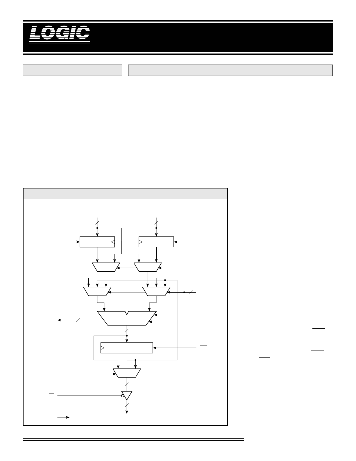
The L4C383 operates on two 16-bit
operands (A and B) and produces a 16-
L4C383 BLOCK DIAGRAM
B15-B
FFFF
0
H
ENA
A15-A
0
16 16
A REGISTER B REGISTER
FFFF
H
ENB
FTAB
bit result (F). Five select lines control
the ALU and provide 19 arithmetic and
13 logical functions. Registers are
provided on both the ALU inputs and
the output, but these may be bypassed
under user control. An internal feedback path allows the registered ALU
output to be routed to one or both of
the ALU inputs, accommodating chain
operations and accumulation.
ALU OPERATIONS
The S4–S0 lines specify the operation to
be performed. The ALU functions and
their select codes are shown in Table 1.
ALU STATUS
The ALU provides Overflow and Zero
status bits. A Carry output is also
provided for cascading multiple
devices, however it is only defined for
the 19 arithmetic functions. The ALU
sets the Zero output when all 16 output
bits are zero. The N, C16 and OVF flags
for the arithmetic operations are
defined in Table 2.
N, C
OVF, Z
FTF
OE
CLK
5
S
4-0
OPERAND REGISTERS
The L4C383 has two 16-bit wide input
registers for operands A and B. These
16
4
ALU
16
C
0
registers are rising edge triggered by a
common clock. The A register is
enabled for input by setting the ENA
control LOW, and the B register is
RESULT REGISTER
ENF
enabled for input by setting the ENB
control LOW. When either the ENA
control or ENB control is HIGH, the
data in the corresponding input register
will not change.
16
This architecture allows the L4C383 to
accept arguments from a single 16-bit
16
data bus. For those applications that do
not require registered inputs, both the
TO ALL REGISTERS
F15-F
0
A and B operand registers can be
bypassed with the FTAB control line.
Arithmetic Logic Units
1
08/16/2000–LDS.383-E

DEVICES INCORPORATED
L4C383
16-bit Cascadable ALU (Extended Set)
TABLE 1. ALU FUNCTIONS
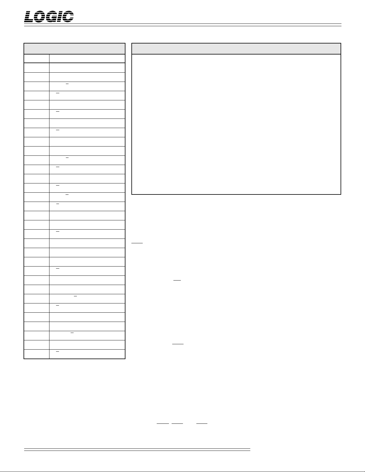
S4-S0 FUNCTION
00000 A + B + C0
00001 A OR B
00010 A + B + C0
00011 A + B + C0
00100 A + C0
00101 A OR F
00110 A – 1 + C0
00111 A + C0
01000 A + F + C0
01001 A OR F
01010 A + F + C0
01011 A + F + C0
01100 F + B + C0
01101 A OR B
01110 F + B + C0
01111 F + B + C0
10000 A XOR B
10001 A AND B
10010 A AND B
10011 A XNOR B
10100 A XOR F
10101 A AND F
10110 A AND F
10111 ALL 1's + C0
11000 B + C0
11001 A AND B
11010 B + C0
11011 B – 1 + C0
11100 F + C0
11101 A OR B
11110 F – 1 + C0
11111 F + C0
When the FTAB control is asserted
(FTAB = HIGH), data is routed
around the A and B input registers;
however, they continue to function
normally via the ENA and ENB
controls. The contents of the input
registers will again be available to the
ALU if the FTAB control is released.
TABLE 2. ALU STATUS FLAGS
Bit Carry Generate = gi =AiBi for i = 0 ... 15
Bit Carry Propagate = pi =Ai + Bi for i = 0 ... 15
P0 =p0
Pi =pi (Pi–1) for i = 1 ... 15
and
G0 =g0
Gi =gi + pi (Gi–1) for i = 1 ... 15
Ci =Gi–1 + Pi–1 (C0) for i = 1 ... 15
then
C16 =G15 + P15C0
OVF = C15 XOR C16
Zero = All Output Bits Equal Zero
N = Sign Bit of ALU Operation
OUTPUT REGISTER
The output of the ALU drives the input of
a 16-bit register. This rising-edgetriggered register is clocked by the same
clock as the input registers. When the
ENF control is LOW, data from the ALU
will be clocked into the output register.
By disabling the output register, intermediate results can be held while loading
new input operands. Three-state drivers
controlled by the OE input allow the
L4C383 to be configured in a single
bidirectional bus system.
The output register can be bypassed by
asserting the FTF control signal (FTF =
HIGH). When the FTF control is asserted,
output data is routed around the output
register, however, it continues to function
normally via the ENF control. The
contents of the output register will again
be available on the output pins if FTF is
released.
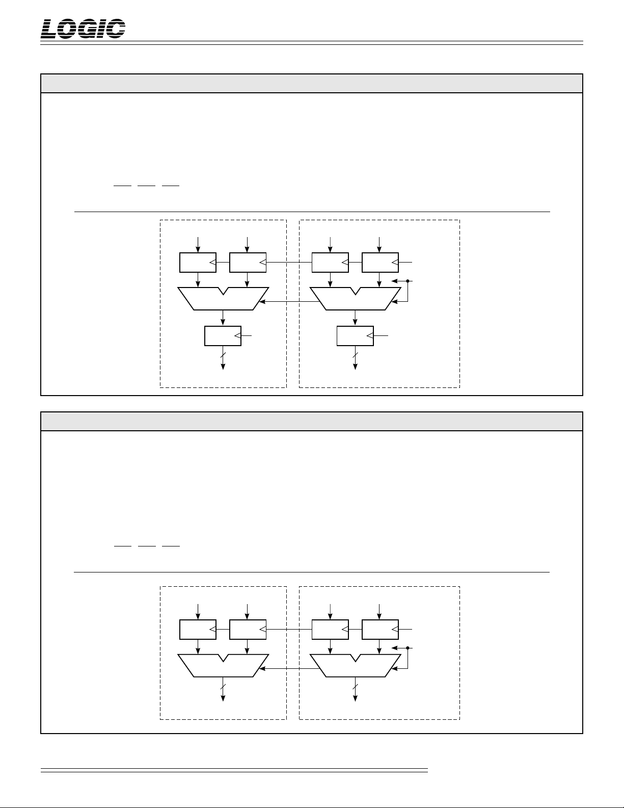
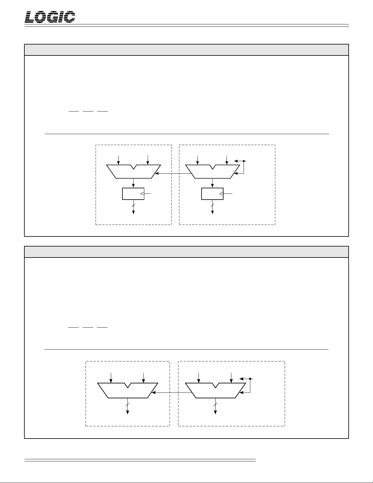
CASCADING THE L4C383
Cascading the L4C383 to 32 bits is
accomplished simply by connecting the
C16 output of the least significant slice to
the C0 input of the most sig-nificant slice.
The S4-S0, ENA, ENB, and ENF lines are
common to both devices. The Zero output
flags should be logically ANDed to
produce the Zero flag for the 32-bit result.
The OVF and C16 outputs of the most
significant slice are valid for the 32-bit
result.
Propagation delay calculations for this
configuration require two steps: First
determine the propagation delay from the
input of interest to the C16 output of the
lower slice. Add this number to the delay
from the C0 input of the upper slice to the
output of interest (of the C0 setup time, if
the F register is used). The sum gives the
overall input-to-output delay (or setup
time) for the 32-bit configuration. This
method gives a conservative result, since
the C16 output is very lightly loaded.
Formulas for calculation of all critical
delays for a 32-bit system are shown in
Figures 4A through 4D.
Cascading to greater than 32 bits can be
accomplished by simply connecting the
C16 output of each slice to the C0 input of
the next more significant slice.
Propagation delays are calculated as
for the 32-bit case, except that the C0
to C16 delays for all intermediate slices
must be added to the overall delay for
each path.
Arithmetic Logic Units
2
08/16/2000–LDS.383-E

DEVICES INCORPORATED
FIGURE 4A. FTAB = 0, FTF = 0
From To Calculated Specification Limit
Clock ➞ F = Same as 16-bit case
Clock ➞ Other = (Clock ➞ C16) + (C0 ➞ Out)
C0 ➞ Other = (C0 ➞ C16) + (C0 ➞ Out)
S4-S0 ➞ Other = (S4-S0 ➞ C16) + (C0 ➞ Out)
A, B Setup time = Same as 16-bit case
C0 Setup time = (C 0 ➞ C16) + (C0 Setup time)
S4-S0 Setup time = (S4-S0 ➞ C16) + (C0 Setup time)
ENA, ENB, ENF Setup time = Same as 16-bit case
Minimum cycle time = (Clock ➞ C16) + (C0 Setup time)
L4C383
16-bit Cascadable ALU (Extended Set)
A31-A16
D
Q
A
MOST
16
SIGNIFICANT
SLICE
FIGURE 4B. FTAB = 0, FTF = 1
From To Calculated Specification Limit
Clock ➞ F = (Clock ➞ C16) + (C0 ➞ F)
Clock ➞ Other = (Clock ➞ C16) + (C0 ➞ Out)
C0 ➞ F = (C0 ➞ C16) + (C0 ➞ F)
C0 ➞ Other = (C0 ➞ C16) + (C0 ➞ Out)
S4-S0 ➞ F = (S4-S0 ➞ C16) + (C0 ➞ F)
S4-S0 ➞ Other = (S4-S0 ➞ C16) + (C0 ➞ Out)
A, B Setup time = Same as 16-bit case
C0 Setup time = (C0 ➞ C16) + (C0 Setup time)
S4-S0 Setup time = (S4-S0 ➞ C16) + (C0 Setup time)
ENA, ENB, ENF Setup time = Same as 16-bit case
Minimum cycle time = (Clock ➞ C16) + (C0 Setup time)
F
D
Q
F31-F16
B31-B16
D
Q
B
0
C
CLOCK CLOCK
A15-A0 B15-B0
D
Q
A
16
C
F
D
Q
16
F15-F0
D
Q
B
C
CLOCK
0–S4
S
C
0,
0
LEAST
SIGNIFICANT
SLICE
MOST
SIGNIFICANT
SLICE
A31-A16
D
Q
A
F
16
F31-F16
B31-B16
D
Q
B
0
C
A15-A0 B15-B0
D
Q
A
16
C
F
16
F15-F0
3
D
Q
B
C
CLOCK
0–S4
S
C
0,
0
LEAST
SIGNIFICANT
SLICE
Arithmetic Logic Units
08/16/2000–LDS.383-E

DEVICES INCORPORATED
FIGURE 4C. FTAB = 1, FTF = 0
From To Calculated Specification Limit
Clock ➞ F = Same as 16-bit case
A, B ➞ Other = (A, B ➞ C16) + (C0 ➞ Out)
C0 ➞ Other = (C0 ➞ C16) + (C0 ➞ Out)
S4-S0 ➞ Other = (S4-S0 ➞ C16) + (C0 ➞ Out)
A, B Setup time = (A, B ➞ C16) + (C0 Setup time)
C0 Setup time = (C0 ➞ C16) + (C0 Setup time)
S4-S0 Setup time = (S4-S0 ➞ C16) + (C0 Setup time)
ENA, ENB, ENF Setup time = Same as 16-bit case
Minimum cycle time = (Clock ➞ C16) + (C0 Setup time)
(F register accumulate loop)
A31-A
A
L4C383
16-bit Cascadable ALU (Extended Set)
16
B31-B
16
B
0
C
F
A15-A
A
16
C
0
B15-B
0
0–S4
S
C
0,
B
0
C
F
MOST
16
SIGNIFICANT
SLICE
FIGURE 4D. FTAB = 1, FTF = 1
From To Calculated Specification Limit
A, B ➞ F = (A, B ➞ C16) + (C0 ➞ F)
A, B ➞ Other = (A, B ➞ C16) + (C0 ➞ Out)
C0 ➞ F = (C0 ➞ C16) + (C0 ➞ F)
C0 ➞ Other = (C0 ➞ C16) + (C0 ➞ Out)
S4-S0 ➞ F = (S4-S0 ➞ C16) + (C0 ➞ F)
S4-S0 ➞ Other = (S4-S0 ➞ C16) + (C0 ➞ Out)
A, B Setup time = (A, B ➞ C16) + (C0 Setup time)
C0 Setup time = (C0 ➞ C16) + (C0 Setup time)
S4-S0 Setup time = (S4-S0 ➞ C16) + (C0 Setup time)
ENA, ENB, ENF Setup time = Same as 16-bit case
Minimum cycle time = (Clock ➞ C16) + (C0 Setup time)
(F register accumulate loop)
D
F31-F
16
D
Q
LEAST
Q
CLOCK CLOCK
SIGNIFICANT
F15-F
16
0
SLICE
MOST
SIGNIFICANT
SLICE
A31-A
A
16
16
F31-F
F
B31-B
16
16
B
0
C
A15-A
A
16
C
0
16
B15-B
0
0–S4
S
C
0,
B
0
C
F
LEAST
SIGNIFICANT
F15-F
0
SLICE
Arithmetic Logic Units
4
08/16/2000–LDS.383-E
 Loading...