LOGIC L29C525PC20, L29C525PC15, L29C525JC15, L29C525JC20 Datasheet

DEVICES INCORPORATED
L29C525
Dual Pipeline Register
Pipeline Registers
03/23/2000–LDS.29C525-G
1
❑❑
❑❑
❑ Dual 8-Deep Pipeline Register
❑❑
❑❑
❑ Configurable to Single 16-Deep
❑❑
❑❑
❑ Low Power CMOS Technology
❑❑
❑❑
❑ Replaces AMD Am29525
❑❑
❑❑
❑ Load, Shift, and Hold Instructions
❑❑
❑❑
❑ Separate Data In and Data Out Pins
❑❑
❑❑
❑ Three-State Outputs
❑❑
❑❑
❑ Package Styles Available:
• 28-pin Plastic DIP
• 28-pin Plastic LCC, J-Lead
FEATURES DESCRIPTION
L29C525
Dual Pipeline Register
DEVICES INCORPORATED
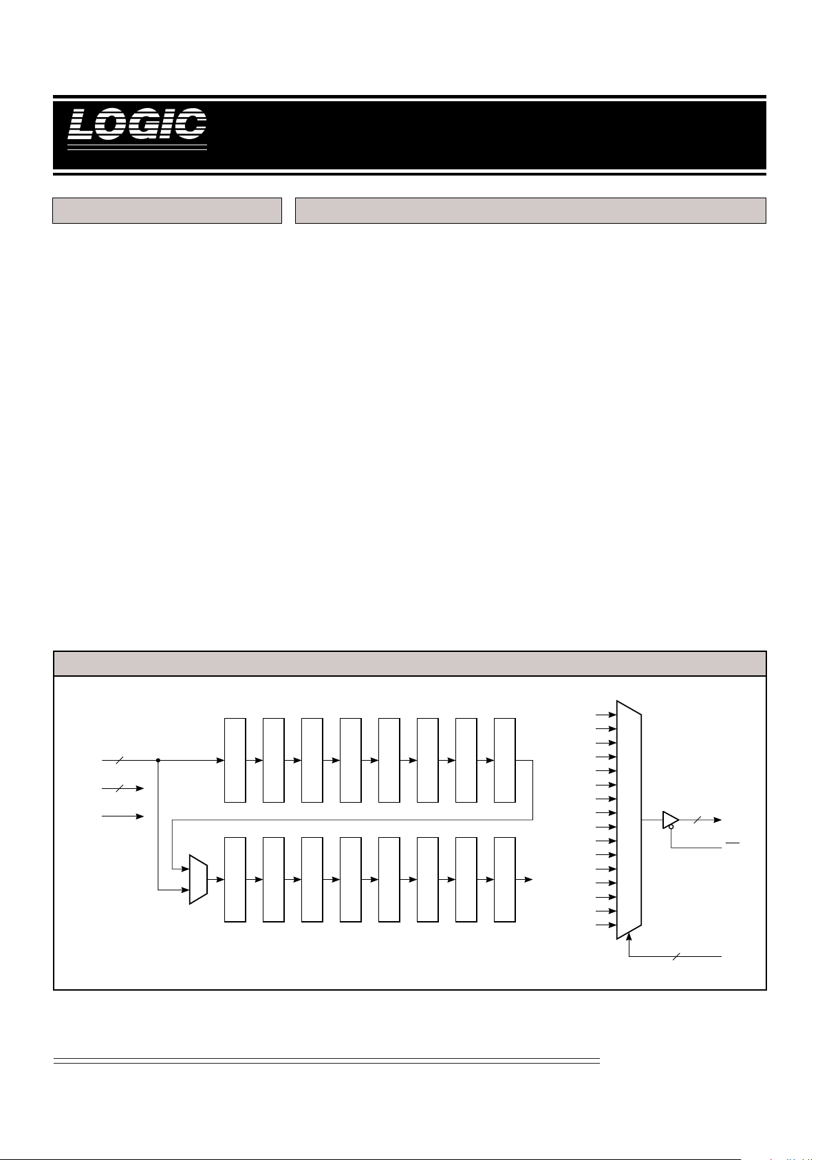
The L29C525 is a high-speed, low
power CMOS pipeline register. It is
pin-for-pin compatible with the AMD
Am29525. The L29C525 can be
configured as two independent 8-level
pipelines or as a single 16-level
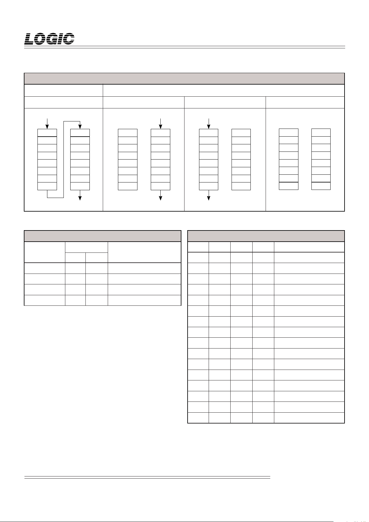
pipeline. The configuration implemented is determined by the instruction code (I1-0) as shown in Table 2.
The I1-0 instruction code controls the
internal routing of data and loading of
each register. For instruction I1-0 = 00
(Push A and B), data applied at the
D7-0 inputs is latched into register A0
on the rising edge of CLK. The
contents of A0 simultaneously move
to register A1, A1 moves to A2, and so
on. The contents of register A7 are
wrapped back to register B0. The
registers on the B side are similarly
shifted, with the contents of register
B7 lost.
Instruction I1-0 = 01 (Push B) acts
similarly to the Push A and B
instruction, except that only the B side
registers are shifted. The input data is
applied to register B0, and the
contents of register B7 are lost. The
contents of the A side registers are
unaffected. Instruction I1-0 = 10 (Push
A) is identical to the Push B
instruction, except that the A side
registers are shifted and the B side
registers are unaffected.
Instruction I1-0 = 11 (Hold) causes no
internal data movement. It is equivalent to preventing the application of a
clock edge to any internal register.
The contents of any of the registers is
selectable at the output through the
use of the S3-0 control inputs. The
independence of the I and S control
lines allows simultaneous reading and
writing. Encoding for the S3-0 controls
is given in Table 3.
L29C525 BLOCK DIAGRAM
8
OE
Y
7-0
D
7-0
I
1-0
CLK
MUX
4
MUX
2
S
3-0
REGISTER A0
REGISTER A1
REGISTER A2
REGISTER A3
REGISTER A4
REGISTER A5
REGISTER A6
REGISTER A7
REGISTER B0
REGISTER B1
REGISTER B2
REGISTER B3
REGISTER B4
REGISTER B5
REGISTER B6
REGISTER B7
A0
A1
A2
A3
A4
A5
A6
A7
B0
B1
B2
B3
B4
B5
B6
B7
8

DEVICES INCORPORATED
L29C525
Dual Pipeline Register
Pipeline Registers
03/27/2000–LDS.29C525-G
2
TABLE 1. REGISTER LOAD OPERATIONS
Single 16 Level Dual 8 Level
Push A and B Push A Hold All RegistersPush B
A0
A1
A2
A3
A4
A5
A6
A7
B0
B1
B2
B3
B4
B5
B6
B7
A0
A1
A2
A3
A4
A5
A6
A7
B0
B1
B2
B3
B4
B5
B6
B7
HOLD
A0
A1
A2
A3
A4
A5
A6
A7
B0
B1
B2
B3
B4
B5
B6
B7
HOLD
A0
A1
A2
A3
A4
A5
A6
A7
B0
B1
B2
B3
B4
B5
B6
B7
HOLDHOLD
TABLE 2. INSTRUCTION SET TABLE 3. OUTPUT SELECT
Inputs
Mnemonics I1 I0 Description
Shift 0 0 Push A and B
LDB 0 1 Push B
LDA 1 0 Push A
HLD 1 1 Hold All Registers
S3 S2 S1 S0 Y7-0
0000A0
0001A1
0010A2
0011A3
0100A4
0101A5
0110A6
0111A7
1000B0
1001B1
1010B2
1011B3
1100B4
1101B5
1110B6
1111B7
 Loading...