

DEVICES INCORPORATED
L29C520/521
4 x 8-bit Multilevel Pipeline Register
Pipeline Registers
08/02/2000–LDS.520/1-P
1
❑❑
❑❑
❑ Four 8-bit Registers
❑❑
❑❑
❑ Implements Double 2-Stage Pipeline
or Single 4-Stage Pipeline Register
❑❑
❑❑
❑ Hold, Shift, and Load Instructions
❑❑
❑❑
❑ Separate Data In and Data Out Pins
❑❑
❑❑
❑ High-Speed, Low Power CMOS
Technology
❑❑
❑❑
❑ Three-State Outputs
❑❑
❑❑
❑ Replaces IDT29FCT520/IDT29FCT521
and AMD Am29520/Am29521
❑❑
❑❑
❑ Package Styles Available:
• 24-pin PDIP
• 28-pin PLCC, J-Lead
FEATURES DESCRIPTION
L29C520/521
4 x 8-bit Multilevel Pipeline Register
DEVICES INCORPORATED
The L29C520 and L29C521 are pin-
for-pin compatible with the
IDT29FCT520/IDT29FCT521 and
AMD Am29520/Am29521, implemented in low power CMOS.
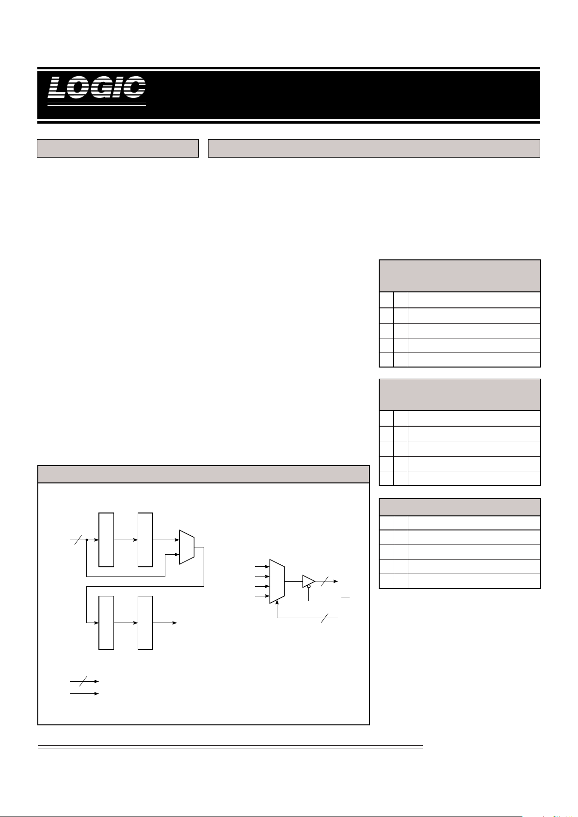
The L29C520 and L29C521 contain
four registers which can be configured
as two independent, 2-level pipelines
or as one 4-level pipeline.
The Instruction pins, I1-0, control the
loading of the registers. For either
device, the registers may be configured as a four-stage delay line, with
data loaded into R1 and shifted
sequentially through R2, R3, and R4.
Also, for the L29C520, data may be
loaded from the inputs into either R1
or R3 with only R2 or R4 shifting. The
L29C521 differs from the L29C520 in
that R2 and R4 remain unchanged
during this type of data load, as
shown in Tables 1 and 2. Finally, I1-0
may be set to prevent any register
from changing.
The S1-0 select lines control a 4-to-1
multiplexer which routes the contents
of any of the registers to the Y output
pins. The independence of the I and S
controls allows simultaneous write
and read operations on different
registers.
S1 S0 Register Selected
L L Register 4
L H Register 3
H L Register 2
H H Register 1
TABLE 3. OUTPUT SELECT
I1 I0 Description
LLD➞R1 R1➞R2 R2➞R3 R3➞R4
L H HOLD HOLD D➞R3 HOLD
HLD➞R1 HOLD HOLD HOLD
H H ALL REGISTERS ON HOLD
TABLE 2.
L29C521 INSTRUCTION TABLE
I1 I0 Description
LLD➞R1 R1➞R2 R2➞R3 R3➞R4
L H HOLD HOLD D➞R3 R3➞R4
HLD➞R1 R1➞R2 HOLD HOLD
H H ALL REGISTERS ON HOLD
TABLE 1.
L29C520 INSTRUCTION TABLE
L29C520/521 BLOCK DIAGRAM
MUX
REG 1
REG 2
REG 3
REG 4
REGISTER 1
REGISTER 2
REGISTER 3
REGISTER 4
MUX
D
8-0
8
8
OE
Y
7-0
S
1-0
I
1-0
CLK
2
2
DEVICES INCORPORATED
L29C520/521
4 x 8-bit Multilevel Pipeline Register
Pipeline Registers
08/02/2000–LDS.520/1-P
2
Storage temperature ........................................................................................................... –65°C to +150°C
Operating ambient temperature........................................................................................... –55°C to +125°C
VCC supply voltage with respect to ground............................................................................ –0.5 V to +7.0V
Input signal with respect to ground ........................................................................................ –3.0 V to +7.0 V
Signal applied to high impedance output ............................................................................... –3.0 V to +7.0 V
Output current into low outputs............................................................................................................. 25 mA
Latchup current ............................................................................................................................... > 400 mA
MAXIMUM RATINGS
Above which useful life may be impaired (Notes 1, 2, 3, 8)
Symbol Parameter Test Condition Min Typ Max Unit
VOH Output High Voltage VCC = Min., IOH = –15.0 mA 2.4 V
VOL Output Low Voltage VCC = Min., IOL = 24.0 mA 0.5 V
VIH Input High Voltage 2.0 VCC V
V IL Input Low Voltage (Note 3) 0.0 0.8 V
IIX Input Current Ground ≤ VIN ≤ VCC (Note 12) ±20 µA
IOZ Output Leakage Current Ground ≤ VOUT ≤ VCC (Note 12) ±20 µA
ICC1 VCC Current, Dynamic (Notes 5, 6) 30 mA
ICC2 VCC Current, Quiescent (Note 7) 1.5 mA
ELECTRICAL CHARACTERISTICS
Over Operating Conditions (Note 4)
OPERATING CONDITIONS
To meet specified electrical and switching characteristics
Mode Temperature Range (Ambient) Supply Voltage
Active Operation, Commercial 0°C to +70°C 4.75 V ≤ VCC ≤ 5.25 V
Active Operation, Military –55°C to +125°C 4.50 V ≤ VCC ≤ 5.50 V
DEVICES INCORPORATED
L29C520/521
4 x 8-bit Multilevel Pipeline Register
Pipeline Registers
08/02/2000–LDS.520/1-P
3
23456789012345
6
23456789012345
6
23456789012345
6
23456789012345
6
23456789012345
6
23456789012345
6
23456789012345
6
23456789012345
6
23456789012345
6
23456789012345
6
23456789012345
6
23456789012345
6
23456789012345
6
23456789012345
6
23456789012345
6
23456789012345
6
23456789012345
6
23456789012345
6
23456789012345
6
23456789012345
6
23456789012345
6
23456789012345
6
23456789012345
6
23456789012345
6
23456789012345
6
23456789012345
6
23456789012345
6
23456789012345
6
23456789012345
6
23456789012345
6
23456789012345
6
23456789012345
6
23456789012345
6
1234567890123456789012345678901212345678901234
1
23456789012345678901234567890121234567890123
4
1
23456789012345678901234567890121234567890123
4
1
23456789012345678901234567890121234567890123
4
1
23456789012345678901234567890121234567890123
4
1
23456789012345678901234567890121234567890123
4
1
23456789012345678901234567890121234567890123
4
1
23456789012345678901234567890121234567890123
4
1
23456789012345678901234567890121234567890123
4
1
23456789012345678901234567890121234567890123
4
1
23456789012345678901234567890121234567890123
4
1
23456789012345678901234567890121234567890123
4
1
23456789012345678901234567890121234567890123
4
1
23456789012345678901234567890121234567890123
4
1
23456789012345678901234567890121234567890123
4
1
23456789012345678901234567890121234567890123
4
1
23456789012345678901234567890121234567890123
4
1
23456789012345678901234567890121234567890123
4
1
23456789012345678901234567890121234567890123
4
1
23456789012345678901234567890121234567890123
4
1
23456789012345678901234567890121234567890123
4
1
23456789012345678901234567890121234567890123
4
1
23456789012345678901234567890121234567890123
4
1
23456789012345678901234567890121234567890123
4
1
23456789012345678901234567890121234567890123
4
1
23456789012345678901234567890121234567890123
4
1
23456789012345678901234567890121234567890123
4
1
23456789012345678901234567890121234567890123
4
1
23456789012345678901234567890121234567890123
4
1
23456789012345678901234567890121234567890123
4
1
23456789012345678901234567890121234567890123
4
1
23456789012345678901234567890121234567890123
4
1
23456789012345678901234567890121234567890123
4
1
23456789012345678901234567890121234567890123
4
1234567890123456789012345678901212345678901234
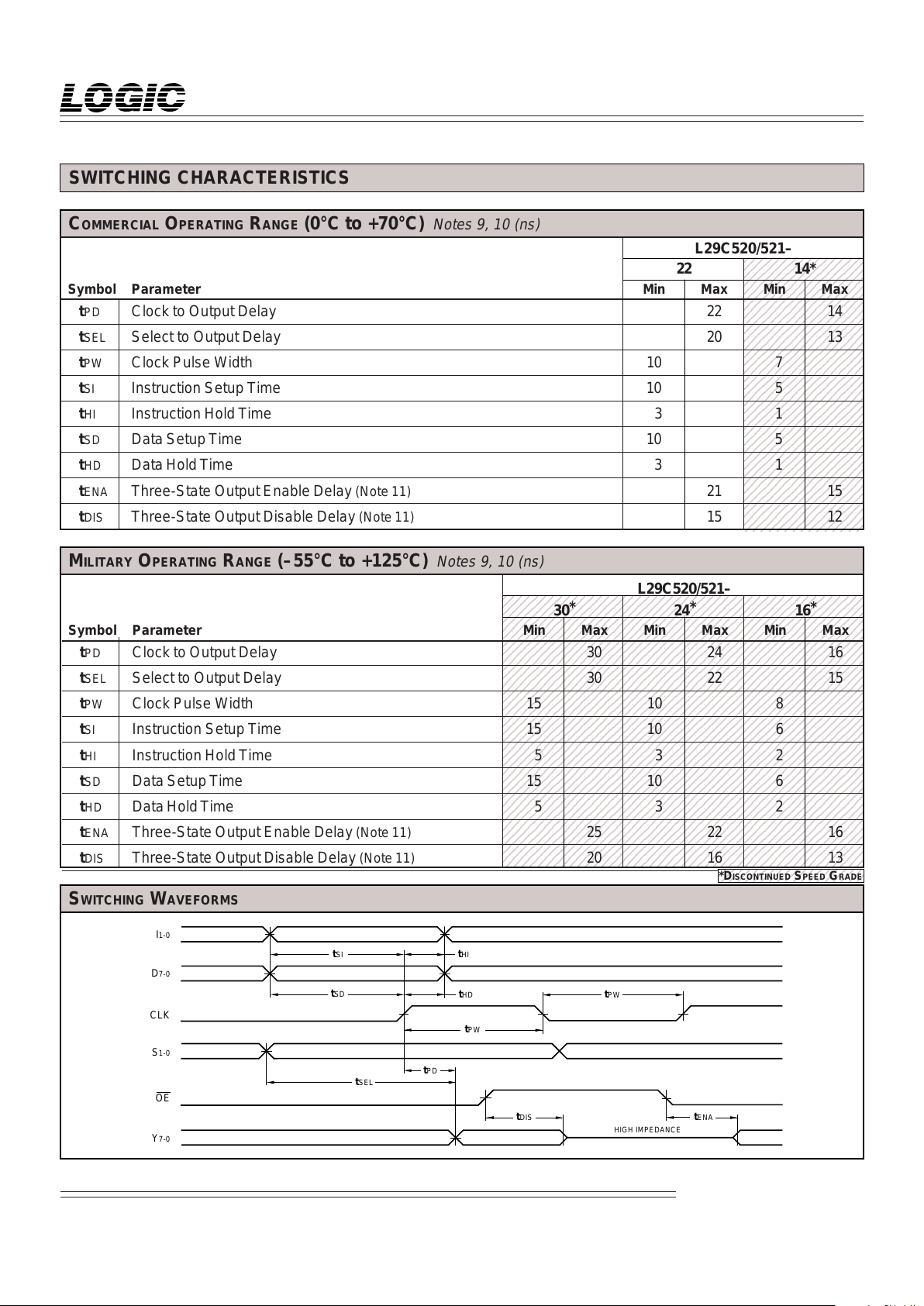
L29C520/521–
22 14*
Symbol Parameter Min M ax Min M ax
tPD Clock to Output Delay 22 14
tSEL Select to Output Delay 20 13
tPW Clock Pulse Width 10 7
tSI Instruction Setup Time 10 5
tHI Instruction Hold Time 3 1
tSD Data Setup Time 10 5
tHD Data Hold Time 3 1
tENA Three-State Output Enable Delay (Note 11) 21 15
tDIS Three-State Output Disable Delay (Note 11) 15 12
COMMERCIAL OPERATING RANGE (0°C to +70°C)
Notes 9, 10 (ns)
SWITCHING CHARACTERISTICS
L29C520/521–
30
*
24
*
16
*
Symbol Parameter Min Max Min Max Min Max
tPD Clock to Output Delay 30 24 16
tSEL Select to Output Delay 30 22 15
tPW Clock Pulse Width 15 10 8
tSI Instruction Setup Time 15 1 0 6
tHI Instruction Hold Time 5 3 2
tSD Data Setup Time 15 1 0 6
tHD Data Hold Time 5 3 2
tENA Three-State Output Enable Delay (Note 11) 25 22 16
tDIS Three-State Output Disable Delay (Note 11) 20 16 13
MILITARY OPERATING RANGE (–55°C to +125°C)
Notes 9, 10 (ns)
SWITCHING WAVEFORMS
HIGH IMPEDANCE
t
ENA
t
DIS
t
PW
t
SI
t
SD
D
7-0
CLK
OE
t
PD
t
HD
t
HI
t
PW
t
SEL
I
1-0
S
1-0
Y
7-0
*DISCONTINUED SPEED GRADE

DEVICES INCORPORATED
L29C520/521
4 x 8-bit Multilevel Pipeline Register
Pipeline Registers
08/02/2000–LDS.520/1-P
4
1. Maximum Ratings indicate stress
specifications only. Functional operation of these products at values beyond
those indicated in the Operating Conditions table is not implied. Exposure to
maximum rating conditions for extended periods may affect reliability.
2. The products described by this specification include internal circuitry designed to protect the chip from damaging substrate injection currents and accumulations of static charge. Nevertheless, conventional precautions should
be observed during storage, handling,
and use of these circuits in order to
avoid exposure to excessive electrical
stress values.
3. This device provides hard clamping of
transient undershoot and overshoot. Input levels below ground or above VCC
will be clamped beginning at –0.6 V and
VCC + 0.6 V. The device can withstand
indefinite operation with inputs in the
range of –0.5 V to +7.0 V. Device operation will not be adversely affected, however, input current levels will be well in
excess of 100 mA.
4. Actual test conditions may vary from
those designated but operation is guaranteed as specified.
5. Supply current for a given application can be accurately approximated by:
where
N = total number of device outputs
C = capacitive load per output
V = supply voltage
F = clock frequency
6. Tested with all outputs changing every cycle and no load, at a 5 MHz clock
rate.
7. Tested with all inputs within 0.1 V of
VCC or Ground, no load.
8. These parameters are guaranteed
but not 100% tested.
NCV F
4
2
NOTES
9. AC specifications are tested with
input transition times less than 3 ns,
output reference levels of 1.5 V (except
tDIS test), and input levels of nominally
0 to 3.0 V. Output loading may be a
resistive divider which provides for
specified IOH and IOL at an output
voltage of VOH min and VOL max
respectively. Alternatively, a diode
bridge with upper and lower current
sources of IOH and IOL respectively,
and a balancing voltage of 1.5 V may be
used. Parasitic capacitance is 30 pF
minimum, and may be distributed.
This device has high-speed outputs capable of large instantaneous current
pulses and fast turn-on/turn-off times.
As a result, care must be exercised in the
testing of this device. The following
measures are recommended:
a. A 0.1 µF ceramic capacitor should be
installed between VCC and Ground
leads as close to the Device Under Test
(DUT) as possible. Similar capacitors
should be installed between device VCC
and the tester common, and device
ground and tester common.
b. Ground and VCC supply planes
must be brought directly to the DUT
socket or contactor fingers.
c. Input voltages should be adjusted to
compensate for inductive ground and VCC
noise to maintain required DUT input
levels relative to the DUT ground pin.
10. Each parameter is shown as a minimum or maximum value. Input requirements are specified from the point
of view of the external system driving
the chip. Setup time, for example, is
specified as a minimum since the external system must supply at least that
much time to meet the worst-case requirements of all parts. Responses from
the internal circuitry are specified from
the point of view of the device. Output
delay, for example, is specified as a
maximum since worst-case operation of
any device always provides data within
that time.
11. For the tENA test, the transition is
measured to the 1.5 V crossing point
with datasheet loads. For the tDIS test,
the transition is measured to the
±200mV level from the measured
steady-state output voltage with
±10mA loads. The balancing voltage, VTH, is set at 3.5 V for Z-to-0
and 0-to-Z tests, and set at 0 V for Zto-1 and 1-to-Z tests.
12. These parameters are only tested at
the high temperature extreme, which is
the worst case for leakage current.
S1
I
OH
I
OL
V
TH
C
L
DUT
OE
0.2 V
t
DIS
t
ENA
0.2 V
1.5 V 1.5 V
3.5V Vth
1
Z
0
Z
Z
1
Z
0
1.5 V
1.5 V
0V Vth
VOL*
V
OH
*
V
OL
*
V
OH
*
Measured V
OL
with IOH = –10mA and IOL = 10mA
Measured V
OH
with IOH = –10mA and IOL = 10mA
FIGURE B. THRESHOLD LEVELS
FIGURE A. OUTPUT LOADING CIRCUIT

DEVICES INCORPORATED
L29C520/521
4 x 8-bit Multilevel Pipeline Register
Pipeline Registers
08/02/2000–LDS.520/1-P
5
0°C to +70°C — COMMERCIAL SCREENING
–55°C to +125°C — MIL-STD-883 COMPLIANT
–55°C to +125°C — COMMERCIAL SCREENING
24-pin — 0.3" wide 28-pin
1
2
3
4
5
6
7
8
9
10
11
12
24
23
22
21
20
19
18
17
16
15
14
13
I
0
I
1
D
0
D
1
D
2
D
3
D
4
D
5
D
6
D
7
CLK
GND
V
CC
S
0
S
1
Y
0
Y
1
Y
2
Y
3
Y
4
Y
5
Y
6
Y
7
OE
5
6
7
8
9
10
11
25
24
23
22
21
20
19
26
Top
View
27
12 17 18
4
28312
13 14 15 16
NC
Y
0
Y
1
Y
2
Y
3
Y
4
Y
5
D
1
D
2
D
3
D
4
D
5
D
6
NC
D7
CLK
GND
OE
Y
7
Y6
NC
NC
D
0
I1I0VCCS0S1
L29C520 — ORDERING INFORMATION
Plastic DIP
(P2)
L29C520PC22
Plastic J-Lead Chip Carrier
(J4)
L29C520JC22
Speed
22 ns

DEVICES INCORPORATED
L29C520/521
4 x 8-bit Multilevel Pipeline Register
Pipeline Registers
08/02/2000–LDS.520/1-P
6
23456789012345678901234567890121234567890123456
7
23456789012345678901234567890121234567890123456
7
23456789012345678901234567890121234567890123456
7
23456789012345678901234567890121234567890123456
7
23456789012345678901234567890121234567890123456
7
23456789012345678901234567890121234567890123456
7
23456789012345678901234567890121234567890123456
7
23456789012345678901234567890121234567890123456
7
23456789012345678901234567890121234567890123456
7
23456789012345678901234567890121234567890123456
7
23456789012345678901234567890121234567890123456
7
23456789012345678901234567890121234567890123456
7
23456789012345678901234567890121234567890123456
7
23456789012345678901234567890121234567890123456
7
23456789012345678901234567890121234567890123456
7
23456789012345678901234567890121234567890123456
7
23456789012345678901234567890121234567890123456
7
23456789012345678901234567890121234567890123456
7
23456789012345678901234567890121234567890123456
7
23456789012345678901234567890121234567890123456
7
23456789012345678901234567890121234567890123456
7
23456789012345678901234567890121234567890123456
7
23456789012345678901234567890121234567890123456
7
23456789012345678901234567890121234567890123456
7
23456789012345678901234567890121234567890123456
7
23456789012345678901234567890121234567890123456
7
23456789012345678901234567890121234567890123456
7
23456789012345678901234567890121234567890123456
7
23456789012345678901234567890121234567890123456
7
23456789012345678901234567890121234567890123456
7
23456789012345678901234567890121234567890123456
7
23456789012345678901234567890121234567890123456
7
23456789012345678901234567890121234567890123456
7
23456789012345678901234567890121234567890123456
7
23456789012345678901234567890121234567890123456
7
23456789012345678901234567890121234567890123456
7
23456789012345678901234567890121234567890123456
7
23456789012345678901234567890121234567890123456
7
23456789012345678901234567890121234567890123456
7
23456789012345678901234567890121234567890123456
7
23456789012345678901234567890121234567890123456
7
23456789012345678901234567890121234567890123456
7
23456789012345678901234567890121234567890123456
7
23456789012345678901234567890121234567890123456
7
23456789012345678901234567890121234567890123456
7
23456789012345678901234567890121234567890123456
7
23456789012345678901234567890121234567890123456
7
23456789012345678901234567890121234567890123456
7
23456789012345678901234567890121234567890123456
7
23456789012345678901234567890121234567890123456
7
23456789012345678901234567890121234567890123456
7
23456789012345678901234567890121234567890123456
7
23456789012345678901234567890121234567890123456
7
23456789012345678901234567890121234567890123456
7
23456789012345678901234567890121234567890123456
7
23456789012345678901234567890121234567890123456
7
23456789012345678901234567890121234567890123456
7
23456789012345678901234567890121234567890123456
7
23456789012345678901234567890121234567890123456
7
23456789012345678901234567890121234567890123456
7
23456789012345678901234567890121234567890123456
7
23456789012345678901234567890121234567890123456
7
23456789012345678901234567890121234567890123456
7
23456789012345678901234567890121234567890123456
7
23456789012345678901234567890121234567890123456
7
23456789012345678901234567890121234567890123456
7
23456789012345678901234567890121234567890123456
7
23456789012345678901234567890121234567890123456
7
23456789012345678901234567890121234567890123456
7
23456789012345678901234567890121234567890123456
7
23456789012345678901234567890121234567890123456
7
23456789012345678901234567890121234567890123456
7
23456789012345678901234567890121234567890123456
7
23456789012345678901234567890121234567890123456
7
23456789012345678901234567890121234567890123456
7
23456789012345678901234567890121234567890123456
7
23456789012345678901234567890121234567890123456
7
23456789012345678901234567890121234567890123456
7
23456789012345678901234567890121234567890123456
7
23456789012345678901234567890121234567890123456
7
23456789012345678901234567890121234567890123456
7
23456789012345678901234567890121234567890123456
7
23456789012345678901234567890121234567890123456
7
23456789012345678901234567890121234567890123456
7
23456789012345678901234567890121234567890123456
7
23456789012345678901234567890121234567890123456
7
23456789012345678901234567890121234567890123456
7
23456789012345678901234567890121234567890123456
7
23456789012345678901234567890121234567890123456
7
23456789012345678901234567890121234567890123456
7
23456789012345678901234567890121234567890123456
7
23456789012345678901234567890121234567890123456
7
23456789012345678901234567890121234567890123456
7
23456789012345678901234567890121234567890123456
7
23456789012345678901234567890121234567890123456
7
23456789012345678901234567890121234567890123456
7
23456789012345678901234567890121234567890123456
7
23456789012345678901234567890121234567890123456
7
23456789012345678901234567890121234567890123456
7
23456789012345678901234567890121234567890123456
7
23456789012345678901234567890121234567890123456
7
23456789012345678901234567890121234567890123456
7
23456789012345678901234567890121234567890123456
7
23456789012345678901234567890121234567890123456
7
23456789012345678901234567890121234567890123456
7
23456789012345678901234567890121234567890123456
7
23456789012345678901234567890121234567890123456
7
23456789012345678901234567890121234567890123456
7
23456789012345678901234567890121234567890123456
7
23456789012345678901234567890121234567890123456
7
23456789012345678901234567890121234567890123456
7
23456789012345678901234567890121234567890123456
7
23456789012345678901234567890121234567890123456
7
23456789012345678901234567890121234567890123456
7
23456789012345678901234567890121234567890123456
7
23456789012345678901234567890121234567890123456
7
23456789012345678901234567890121234567890123456
7
23456789012345678901234567890121234567890123456
7
23456789012345678901234567890121234567890123456
7
23456789012345678901234567890121234567890123456
7
23456789012345678901234567890121234567890123456
7
23456789012345678901234567890121234567890123456
7
23456789012345678901234567890121234567890123456
7
23456789012345678901234567890121234567890123456
7
23456789012345678901234567890121234567890123456
7
23456789012345678901234567890121234567890123456
7
23456789012345678901234567890121234567890123456
7
23456789012345678901234567890121234567890123456
7
23456789012345678901234567890121234567890123456
7
23456789012345678901234567890121234567890123456
7
23456789012345678901234567890121234567890123456
7
23456789012345678901234567890121234567890123456
7
23456789012345678901234567890121234567890123456
7
23456789012345678901234567890121234567890123456
7
0°C to +70°C — COMMERCIAL SCREENING
–55°C to +125°C — MIL-STD-883 COMPLIANT
–55°C to +125°C — COMMERCIAL SCREENING
I
0
I
1
D
0
D
1
D
2
D
3
D
4
D
5
D
6
D
7
CLK
GND
V
CC
S
0
S
1
Y
0
Y
1
Y
2
Y
3
Y
4
Y
5
Y
6
Y
7
OE
24
23
22
21
20
19
18
17
16
15
14
13
1
2
3
4
5
6
7
8
9
10
11
12
24-pin — 0.209" wide
L29C520 — ORDERING INFORMATION
24-pin
1
2
3
4
5
6
7
8
9
10
11
12
24
23
22
21
20
19
18
17
16
15
14
13
I
0
I
1
D
0
D
1
D
2
D
3
D
4
D
5
D
6
D
7
CLK
GND
V
CC
S
0
S
1
Y
0
Y
1
Y
2
Y
3
Y
4
Y
5
Y
6
Y
7
OE
Speed
22 ns
Ceramic Flatpack
(M1)
Plastic SSOP
(S1)
Discontinued Package Discontinued Package

DEVICES INCORPORATED
L29C520/521
4 x 8-bit Multilevel Pipeline Register
Pipeline Registers
08/02/2000–LDS.520/1-P
7
23456789012345678901234567890121234567890123456
7
23456789012345678901234567890121234567890123456
7
23456789012345678901234567890121234567890123456
7
23456789012345678901234567890121234567890123456
7
23456789012345678901234567890121234567890123456
7
23456789012345678901234567890121234567890123456
7
23456789012345678901234567890121234567890123456
7
23456789012345678901234567890121234567890123456
7
23456789012345678901234567890121234567890123456
7
23456789012345678901234567890121234567890123456
7
23456789012345678901234567890121234567890123456
7
23456789012345678901234567890121234567890123456
7
23456789012345678901234567890121234567890123456
7
23456789012345678901234567890121234567890123456
7
23456789012345678901234567890121234567890123456
7
23456789012345678901234567890121234567890123456
7
23456789012345678901234567890121234567890123456
7
23456789012345678901234567890121234567890123456
7
23456789012345678901234567890121234567890123456
7
23456789012345678901234567890121234567890123456
7
23456789012345678901234567890121234567890123456
7
23456789012345678901234567890121234567890123456
7
23456789012345678901234567890121234567890123456
7
23456789012345678901234567890121234567890123456
7
23456789012345678901234567890121234567890123456
7
23456789012345678901234567890121234567890123456
7
23456789012345678901234567890121234567890123456
7
23456789012345678901234567890121234567890123456
7
23456789012345678901234567890121234567890123456
7
23456789012345678901234567890121234567890123456
7
23456789012345678901234567890121234567890123456
7
23456789012345678901234567890121234567890123456
7
23456789012345678901234567890121234567890123456
7
23456789012345678901234567890121234567890123456
7
23456789012345678901234567890121234567890123456
7
23456789012345678901234567890121234567890123456
7
23456789012345678901234567890121234567890123456
7
23456789012345678901234567890121234567890123456
7
23456789012345678901234567890121234567890123456
7
23456789012345678901234567890121234567890123456
7
23456789012345678901234567890121234567890123456
7
23456789012345678901234567890121234567890123456
7
23456789012345678901234567890121234567890123456
7
23456789012345678901234567890121234567890123456
7
23456789012345678901234567890121234567890123456
7
23456789012345678901234567890121234567890123456
7
23456789012345678901234567890121234567890123456
7
23456789012345678901234567890121234567890123456
7
23456789012345678901234567890121234567890123456
7
23456789012345678901234567890121234567890123456
7
23456789012345678901234567890121234567890123456
7
23456789012345678901234567890121234567890123456
7
23456789012345678901234567890121234567890123456
7
23456789012345678901234567890121234567890123456
7
23456789012345678901234567890121234567890123456
7
23456789012345678901234567890121234567890123456
7
23456789012345678901234567890121234567890123456
7
23456789012345678901234567890121234567890123456
7
23456789012345678901234567890121234567890123456
7
23456789012345678901234567890121234567890123456
7
23456789012345678901234567890121234567890123456
7
23456789012345678901234567890121234567890123456
7
23456789012345678901234567890121234567890123456
7
23456789012345678901234567890121234567890123456
7
23456789012345678901234567890121234567890123456
7
23456789012345678901234567890121234567890123456
7
23456789012345678901234567890121234567890123456
7
0°C to +70°C — COMMERCIAL SCREENING
–55°C to +125°C — MIL-STD-883 COMPLIANT
–55°C to +125°C — COMMERCIAL SCREENING
1
2
3
4
5
6
7
8
9
10
11
12
24
23
22
21
20
19
18
17
16
15
14
13
I
0
I
1
D
0
D
1
D
2
D
3
D
4
D
5
D
6
D
7
CLK
GND
V
CC
S
0
S
1
Y
0
Y
1
Y
2
Y
3
Y
4
Y
5
Y
6
Y
7
OE
5
6
7
8
9
10
11
25
24
23
22
21
20
19
26
Top
View
27
12 17 18
4
28312
13 14 15 16
NC
Y
0
Y
1
Y
2
Y
3
Y
4
Y
5
D
1
D
2
D
3
D
4
D
5
D
6
NC
D7
CLK
GND
OE
Y
7
Y6
NC
NC
D
0
I1I0VCCS0S1
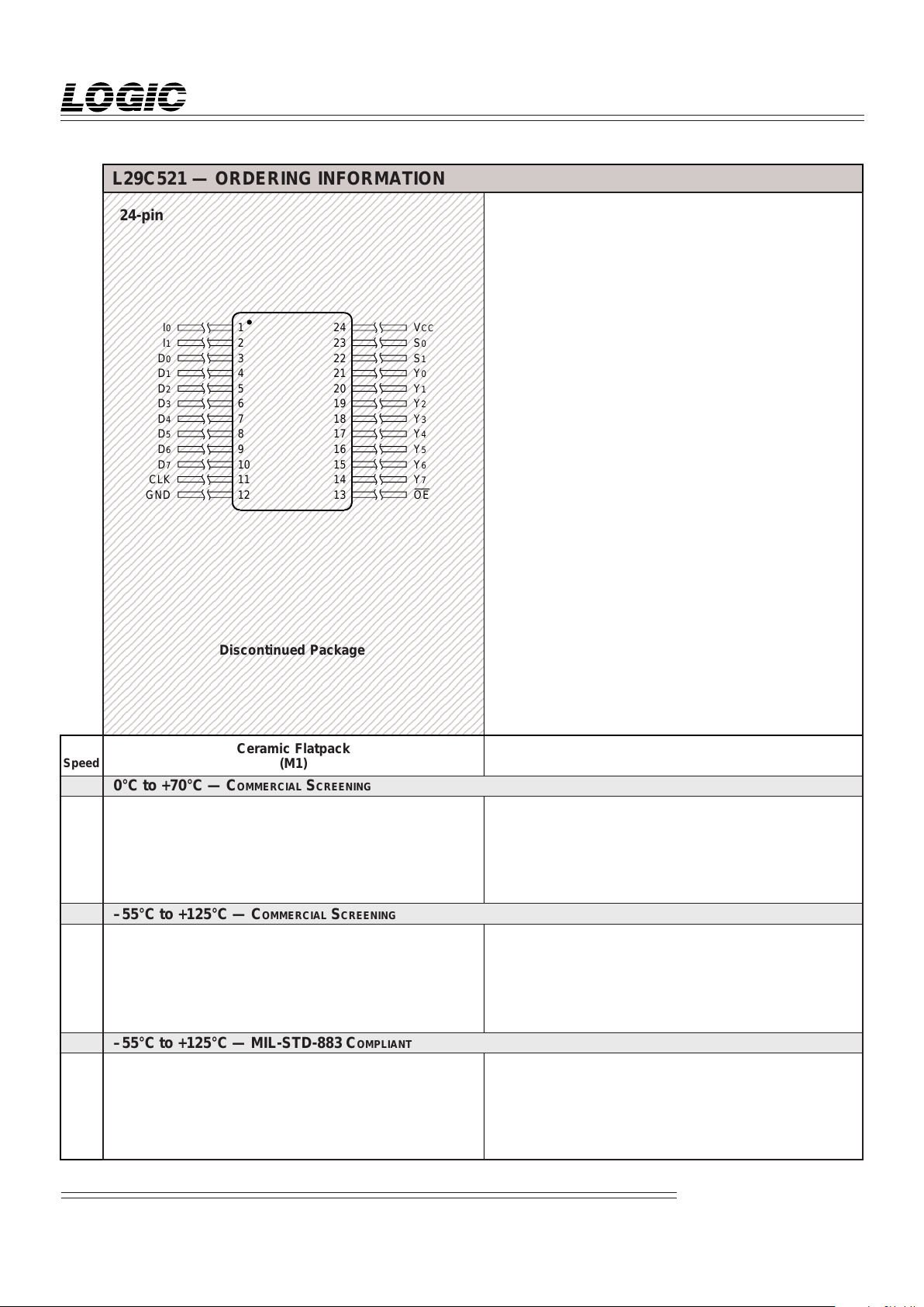
L29C521 — ORDERING INFORMATION
24-pin — 0.3" wide 28-pin
Plastic DIP
(P2)
L29C521PC22
Plastic J-Lead Chip Carrier
(J4)
Speed
22 ns
Discontinued Package
DEVICES INCORPORATED
L29C520/521
4 x 8-bit Multilevel Pipeline Register
Pipeline Registers
08/02/2000–LDS.520/1-P
8
23456789012345678901234567890121234567890123456
7
23456789012345678901234567890121234567890123456
7
23456789012345678901234567890121234567890123456
7
23456789012345678901234567890121234567890123456
7
23456789012345678901234567890121234567890123456
7
23456789012345678901234567890121234567890123456
7
23456789012345678901234567890121234567890123456
7
23456789012345678901234567890121234567890123456
7
23456789012345678901234567890121234567890123456
7
23456789012345678901234567890121234567890123456
7
23456789012345678901234567890121234567890123456
7
23456789012345678901234567890121234567890123456
7
23456789012345678901234567890121234567890123456
7
23456789012345678901234567890121234567890123456
7
23456789012345678901234567890121234567890123456
7
23456789012345678901234567890121234567890123456
7
23456789012345678901234567890121234567890123456
7
23456789012345678901234567890121234567890123456
7
23456789012345678901234567890121234567890123456
7
23456789012345678901234567890121234567890123456
7
23456789012345678901234567890121234567890123456
7
23456789012345678901234567890121234567890123456
7
23456789012345678901234567890121234567890123456
7
23456789012345678901234567890121234567890123456
7
23456789012345678901234567890121234567890123456
7
23456789012345678901234567890121234567890123456
7
23456789012345678901234567890121234567890123456
7
23456789012345678901234567890121234567890123456
7
23456789012345678901234567890121234567890123456
7
23456789012345678901234567890121234567890123456
7
23456789012345678901234567890121234567890123456
7
23456789012345678901234567890121234567890123456
7
23456789012345678901234567890121234567890123456
7
23456789012345678901234567890121234567890123456
7
23456789012345678901234567890121234567890123456
7
23456789012345678901234567890121234567890123456
7
23456789012345678901234567890121234567890123456
7
23456789012345678901234567890121234567890123456
7
23456789012345678901234567890121234567890123456
7
23456789012345678901234567890121234567890123456
7
23456789012345678901234567890121234567890123456
7
23456789012345678901234567890121234567890123456
7
23456789012345678901234567890121234567890123456
7
23456789012345678901234567890121234567890123456
7
23456789012345678901234567890121234567890123456
7
23456789012345678901234567890121234567890123456
7
23456789012345678901234567890121234567890123456
7
23456789012345678901234567890121234567890123456
7
23456789012345678901234567890121234567890123456
7
23456789012345678901234567890121234567890123456
7
23456789012345678901234567890121234567890123456
7
23456789012345678901234567890121234567890123456
7
23456789012345678901234567890121234567890123456
7
23456789012345678901234567890121234567890123456
7
23456789012345678901234567890121234567890123456
7
23456789012345678901234567890121234567890123456
7
23456789012345678901234567890121234567890123456
7
23456789012345678901234567890121234567890123456
7
23456789012345678901234567890121234567890123456
7
23456789012345678901234567890121234567890123456
7
23456789012345678901234567890121234567890123456
7
23456789012345678901234567890121234567890123456
7
23456789012345678901234567890121234567890123456
7
23456789012345678901234567890121234567890123456
7
23456789012345678901234567890121234567890123456
7
23456789012345678901234567890121234567890123456
7
23456789012345678901234567890121234567890123456
7
23456789012345678901234567890121234567890123456
7
23456789012345678901234567890121234567890123456
7
23456789012345678901234567890121234567890123456
7
23456789012345678901234567890121234567890123456
7
0°C to +70°C — COMMERCIAL SCREENING
–55°C to +125°C — MIL-STD-883 COMPLIANT
–55°C to +125°C — COMMERCIAL SCREENING
I
0
I
1
D
0
D
1
D
2
D
3
D
4
D
5
D
6
D
7
CLK
GND
V
CC
S
0
S
1
Y
0
Y
1
Y
2
Y
3
Y
4
Y
5
Y
6
Y
7
OE
24
23
22
21
20
19
18
17
16
15
14
13
1
2
3
4
5
6
7
8
9
10
11
12
24-pin
L29C521 — ORDERING INFORMATION
Speed
Ceramic Flatpack
(M1)
Discontinued Package
 Loading...