

Page 1
DEVICES INCORPORATED
L2340
Digital Synthesizer
L2340
DEVICES INCORPORATED
FEATURES DESCRIPTION
❑❑
❑ Digital Waveform Synthesis at
❑❑
50 MHz
❑❑
❑ 24-Bit Polar Phase Angle Accuracy
❑❑
❑❑
❑ User-selectable Waveform Synthesis,
❑❑
Frequency Modulation, or Phase
Modulation.
❑❑
❑ Amplitude Input for Amplitude
❑❑
Modulation and Gain Adjustment.
❑❑
❑ Replaces TRW/Raytheon/Fairchild
❑❑
TMC2340A
❑❑
❑ 120-pin PQFP
❑❑
The L2340 is a digital synthesizer that
performs waveform synthesis, modulation, and demodulation.
The L2340 automatically generates
quadrature matched pairs of 16-bit
sine and cosine waves in DACcompatible 16-bit offset binary format
with15-bit amplitude and 32-bit phase
inputs.
Output waveforms can be phase or
frequency modulated. Digital output
frequencies are restricted to the
Nyquist limit.
Functional Description
The L2340 converts Polar (Phase and
Magnitude) data into Rectangular
(Cartesian) coordinates. The user
Digital Synthesizer
selects the numeric format. A valid
transformed result is seen at the
output after 22 clock cycles and will
continue upon every clock cycle
thereafter.
15-bit amplitude and 32-bit phase data
are input into the L2340 to produce an
output of 16-bit rectangular data. The
user may select the data format to
either 16-bit offset binary or 15-bit
unsigned magnitude format. High
accuracy phase increment values with
minimal accumulation error is accomplished by use of a 32-bit phase
accumulator.
The phase accumulator structure
supports frequency or phase modulation and is selected by ENP1-0 and
accumulator controls FM and PM.
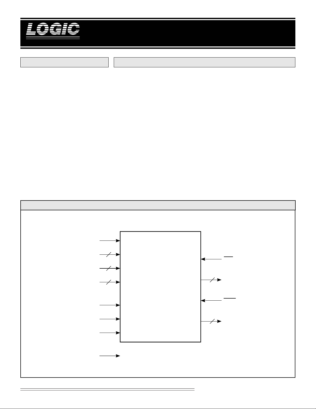
L2340 BLOCK DIAGRAM
ENP
ENA
AM
PH
OBIQ
14-0
1-0
31-0
FM
PM
15
32
2
16
OEI
I
15-0
Digital
Synthesizer
OEQ
16
Q
15-0
CLK
Special Arithmetic Functions
1
08/16/2000–LDS.2340-E
Page 2
DEVICES INCORPORATED
L2340
Digital Synthesizer
L2340 FUNCTIONAL BLOCK DIAGRAM
14-0
OBIQ
OEI
15
15
15
16
16
AM
ENA ENP
32
AM
TRANSFORM
*
PROCESSOR
PH
MC
31-0
Outputs
I15-0 — x-coordinate Data Output
1-0
FM PM
I15-0 is the 16-bit Cartesian x-coordi-
32
2
nate Data output port. When OEI is
HIGH, I15-0 is forced into the highimpedance state. I15 is forced HIGH if
OBIQ is LOW.
Q15-0 — y-coordinate Data Output
32
PM
32
Q15-0 is the 16-bit Cartesian y-coordinate Data output port. When OEQ is
HIGH, Q15-0 is forced into the highimpedance state. Q15 is forced HIGH
if OBIQ is LOW.
FM
24
32
Controls
ENA — Amplitude Modulation Data
Input Enable
24
When ENA is HIGH, AM is latched
into the input register on the rising
16
edge of clock. When ENA is LOW, the
value stored in the register is unchanged.
16
OEQ
ENP1-0 — Phase Modulation Data Input
Control
I
15-0
REQUIRES 18 CYCLES TO COMPLETE AND IS FULLY PIPELINED*
SIGNAL DEFINITIONS
Power
Vcc and GND
+5V power supply. All pins must be
connected.
Clock
CLK — Master Clock
The rising edge of CLK strobes all
enabled registers.
Q
15-0
Inputs
AM14-0 — Amplitude Modulation Data
Input
AM14-0 is the 15-bit Amplitude
Modulation Data input port. AM14-0
is latched on the rising edge of CLK.
PH31-0 — Phase Angle Data Input
PH31-0 is the 32-bit Phase Angle Data
input port. Input phase accumulators
are loaded through this port into
registers enabled by ENP1-0. PH31-0 is
latched on the rising edge of CLK.
ENP1-0 is the 2-bit Phase Modulation
Data Input Control that determines
one of the four modes shown in Table
1. ‘M’ is the Modulation Register and
‘C’ is the Carrier Register as shown in
the Functional Block Diagram.
TABLE 1. REGISTER OPERATION
ENP1-0 Configuration
0 0 No registers enabled, current data held
0 1 M register input enabled, C data held
1 0 C register input enabled, M data held
1 1 M register = 0, C register input enabled
TABLE 2. ACCUMULATOR CONTROL
FM PM Configuration
00No accumulation (normal operation)
01PM accumulator path enabled
10FM accumulator path enabled
11Logical OR of PM and FM (Nonsensical)
Special Arithmetic Functions
2
08/16/2000–LDS.2340-E
Page 3
DEVICES INCORPORATED
L2340
Digital Synthesizer
FM, PM — Frequency Modulation,
Phase Modulation Control
FM and PM is the 2-bit Frequency
Modulation/Phase Modulation
Control that determines one of the
four modes shown in Table 2. When
full-scale is exceeded, the accumulator
will roll over correctly allowing
continuous phase accumulation
through 2π radians.
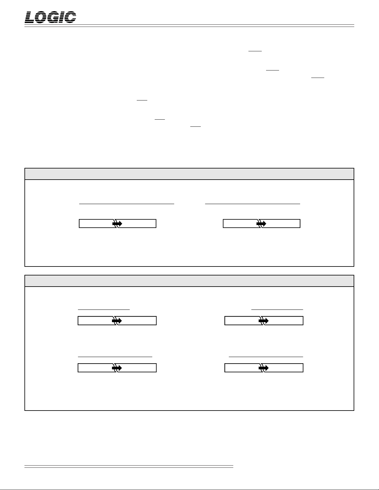
FIGURE 1A.INPUT FORMATS
AM PH
14 13 12 2 1 0
2142132
12
OBIQ — Data Input/Output Format
Select
When OBIQ is HIGH, offset binary
format is selected. When OBIQ is
LOW, unsigned format is selected.
OEI — x-coordinate Data Output
Enable
When OEI is LOW, I15-0 is enabled for
data output. When OEI is HIGH, I15-0
is placed in a high-impedance state.
(RTP = 0)
Fract. Unsigned Mag./Two's Comp.Integer Unsigned Magnitude
22212
0
OEQ — y-coordinate Data Output
Enable
When OEQ is LOW, Q15-0 is enabled
for data output. When OEQ is HIGH,
Q15-0 is placed in a high-impedance
state.
31 30 29 2 1 0
*±202–12
–2
–292–302–31
2
*±20 denotes two's complement sign or highest magnitude bit. Since phase angles are modulo 2π
and phase accumulator is modulo 2
FIGURE 1B.OUTPUT FORMATS
IQ
14 13 12 2 1 0
14213212
2
15 14 13 2 1 0
14213
NS 2
NS denotes negative sign. (i.e. '1' negates the number)
32
, this bit may be regarded as ±π
.
Integer Unsigned Magnitude (OBIQ = 0)
14 13 12 2 1 0
22212
0
14213212
2
Offset Binary (OBIQ = 1)
15 14 13 2 1 0
22212
0
NS 2
14213
22212
22212
0
0
Special Arithmetic Functions
3
08/16/2000–LDS.2340-E
Page 4
DEVICES INCORPORATED
L2340
Digital Synthesizer
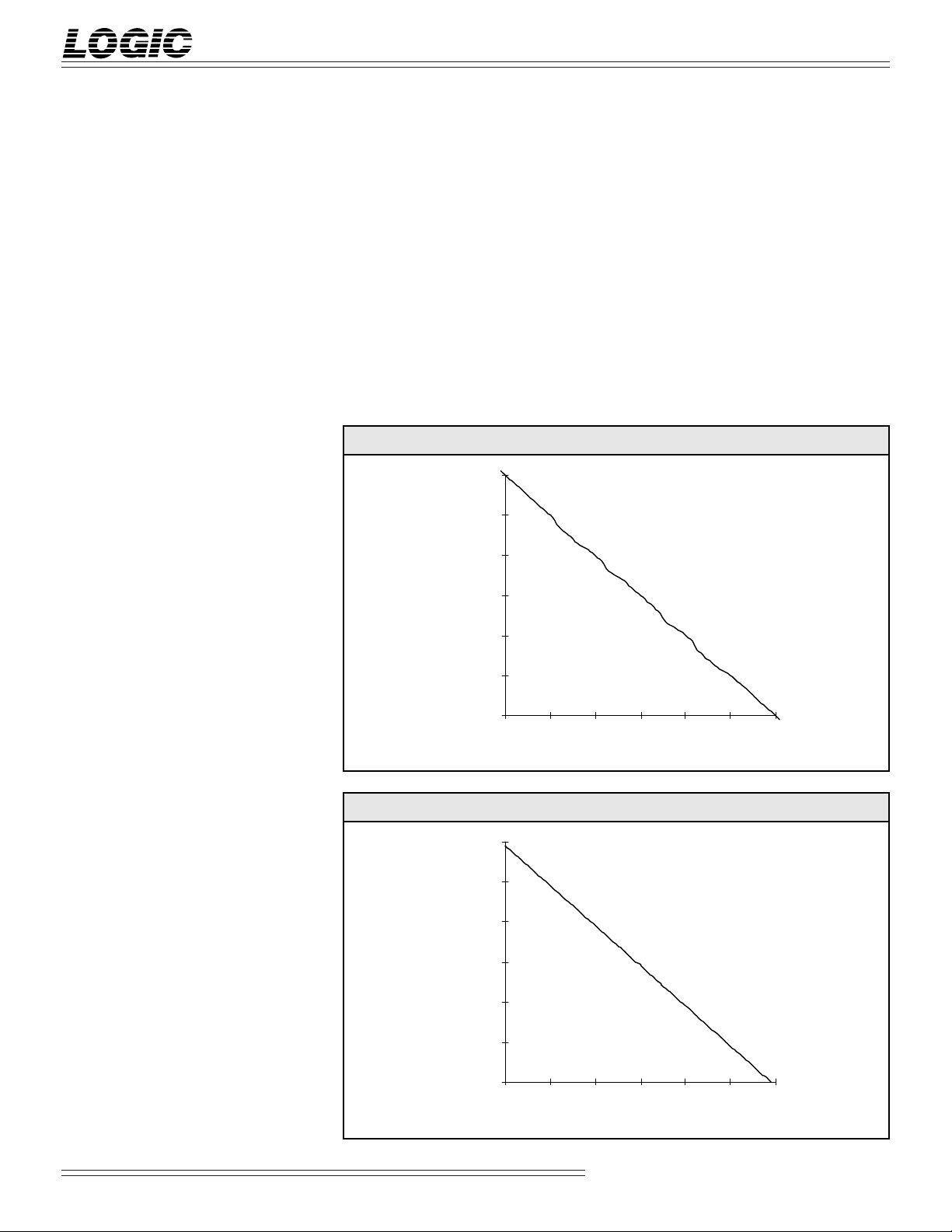
Circle Test
When performing a coordinate
transformation, inaccuracies are
introduced by a combination of
quantization and approximation
errors. The accuracy of a coordinate
transformer is dependent on the
word length used for the input
variables, the word length used for
internal calculations, as well as the
number of iterations or steps performed. Truncation errors are due
to the finite word length and approximation errors are due to the
finite number of iterations. For
example, in the case of performing a
polar-to-rectangular transformation,
the accuracy of the rotation will be
determined by how closely the input
rotation angle was approximated by
the summation of sub-rotation
angles.
In this study, we compare how
accurately a coordinate transformer
with a 16-bit internal processor
versus a 24-bit internal processor
can calculate all the coordinates of a
circle. By setting the radius to
7FFFH, θ is incremented using the
accumulator of the L2340 in steps of
0000 4000H until all the points of a
full circle are calculated into rectangular coordinates.
error will introduce noise when
performing waveform sythesis,
modulation, and demodulation.
Data values for Figure 2 and Figure
3 are shown in Table 3. By looking
at these values, we observe the step
resolution on a 16-bit internal
processor is not 1 unit in the x and
y. In most cases, the minimum step
resolution is 2 units in the x and y.
On the other hand, step resolution
on a 24-bit internal processor is 1
unit in the x and y thus resulting in
greater accuracy.
The minimum theoretical angle
resolution that could be produced is
0.00175° when x = 7FFFH and y = 1H.
A 16-bit internal processor can
produce a minimum angle resolution of only 0.00549° and will not be
able to properly calculate the
theoretical minimum angle resolution. On the other hand, a 24-bit
internal processor can produce a
minimum angle resolution of
0.00002° and could therefore properly calculate the theoretical minimum angle resolution.
FIGURE 2. CIRCLE TEST RESULT NEAR 45° (16-BIT INTERNAL PROCES-
SOR)
23200
23190
23180
23170
Y
23160
23150
23140
23140 23150 23160 23170 23180 23190 23200
X
The resulting rectangular coordinates were plotted and graphed. A
graphical representation of the
resulting vectors for both 16-bit and
24-bit internal processors are compared at 45°. Theoretically, a
perfect circle is the desired output
but when the resulting vectors from
a coordinate transformer with 16-bit
internal processor are graphed and
displayed as shown in Figure 2, we
see significant errors due to the
inherent properties of a digital
synthesizer. In comparison, the 24bit internal processor proves to be
significantly more accurate than a
16-bit internal processor due to
minimization of truncation errors.
In many applications, this margin of
FIGURE 3. CIRCLE TEST RESULT NEAR 45° (24-BIT INTERNAL PROCES-
SOR)
23200
23190
23180
23170
Y
23160
23150
23140
23140 23150 23160 23170 23180 23190 23200
X
Special Arithmetic Functions
4
08/16/2000–LDS.2340-E
Page 5

DEVICES INCORPORATED
TABLE 3. RESULTANT DATA VALUES OF CIRCLE TEST NEAR 45°
16-bit Internal Processor 24-bit Internal Processor
x x (HEX) y y (HEX) x x (HEX) y y (HEX)
23201 5AA1 23139 5A63 23199 5A9F 23140 5A64
23199 5A9F 23141 5A65 23198 5A9E 23141 5A65
23199 5A9F 23141 5A65 23198 5A9E 23141 5A65
23199 5A9F 23141 5A65 23197 5A9D 23142 5A66
23199 5A9F 23141 5A65 23197 5A9D 23142 5A66
23197 5A9D 23143 5A67 23196 5A9C 23143 5A67
23197 5A9D 23143 5A67 23196 5A9C 23143 5A67
23197 5A9D 23143 5A67 23195 5A9B 23144 5A68
23197 5A9D 23143 5A67 23194 5A9A 23145 5A69
23195 5A9B 23145 5A69 23194 5A9A 23145 5A69
23195 5A9B 23145 5A69 23194 5A9A 23145 5A69
23195 5A9B 23145 5A69 23193 5A99 23146 5A6A
23195 5A9B 23145 5A69 23192 5A98 23147 5A6B
23192 5A98 23148 5A6C 23191 5A97 23148 5A6C
23192 5A98 03148 5A6C 23191 5A97 23148 5A6C
23192 5A98 23148 5A6C 23191 5A97 23148 5A6C
23192 5A98 23148 5A6C 23190 5A96 23149 5A6D
23190 5A96 23150 5A6E 23189 5A95 23150 5A6E
23190 5A96 23150 5A6E 23189 5A95 23150 5A6E
23190 5A96 23150 5A6E 23189 5A95 23150 5A6E
23190 5A96 23150 5A6E 23188 5A94 23151 5A6F
23187 5A93 23152 5A70 23187 5A93 23152 5A70
23187 5A93 23152 5A70 23186 5A92 23153 5A71
23187 5A93 23152 5A70 23186 5A92 23153 5A71
23187 5A93 23152 5A70 23186 5A92 23153 5A71
23185 5A91 23154 5A72 23185 5A91 23154 5A72
23185 5A91 23154 5A72 23184 5A90 23155 5A73
23185 5A91 23154 5A72 23184 5A90 23155 5A73
23185 5A91 23154 5A72 23184 5A90 23155 5A73
23183 5A8F 23156 5A74 23183 5A8F 23156 5A74
L2340
Digital Synthesizer
Special Arithmetic Functions
5
08/16/2000–LDS.2340-E
Page 6

DEVICES INCORPORATED
L2340
Digital Synthesizer
MAXIMUM RATINGS
Storage temperature ........................................................................................................... –65°C to +150°C
Operating ambient temperature........................................................................................... –55°C to +125°C
VCC supply voltage with respect to ground............................................................................ –0.5 V to +7.0V
Input signal with respect to ground ............................................................................... –0.5 V to VCC + 0.5 V
Signal applied to high impedance output ...................................................................... –0.5 V to VCC + 0.5 V
Output current into low outputs............................................................................................................. 25 mA
Latchup current ............................................................................................................................... > 400 mA
OPERATING CONDITIONS
Active Operation, Commercial 0°C to +70°C 4.75 V ≤ VCC ≤ 5.25 V
Active Operation, Military –55°C to +125°C 4.50 V ≤ VCC ≤ 5.50 V
ELECTRICAL CHARACTERISTICS
Above which useful life may be impaired (Notes 1, 2, 3, 8)
To meet specified electrical and switching characteristics
Mode Temperature Range (Ambient) Supply Voltage
Over Operating Conditions (Note 4)
Symbol Parameter Test Condition Min Typ Max Unit
VOH Output High Voltage VCC = Min., IOH = –2.0 mA 2.4 V
VOL Output Low Voltage VCC = Min., IOL = 4.0 mA 0.4 V
VIH Input High Voltage 2.0 VCC V
V IL Input Low Voltage (Note 3) 0.0 0.8 V
IIX Input Current Ground ≤ VIN ≤ VCC (Note 12) ±10 µA
IOZ Output Leakage Current Ground ≤ VOUT ≤ VCC (Note 12) ±10 µA
ICC1 VCC Current, Dynamic (Notes 5, 6) 95 mA
ICC2 VCC Current, Quiescent (Note 7) 5mA
CIN Input Capacitance TA = 25°C, f = 1 MHz 10 pF
COUT Output Capacitance TA = 25°C, f = 1 MHz 10 pF
Special Arithmetic Functions
6
08/16/2000–LDS.2340-E
Page 7

DEVICES INCORPORATED
1234567890123456789012345678901212345678901234
1
4
1
4
1
4
1
4
1
4
1
4
1
4
1
4
1
4
1
4
1
4
1
4
1
4
1
4
1
4
1
4
1
4
1
4
1
4
1
4
1
4
1
4
1
4
1
4
1
4
1
4
1
4
1
4
1
4
1
4
1234567890123456789012345678901212345678901234
1234567890123456789012345678901
1
1
1
1
1
1
1
1
1
1
1
1
1
1
1
1
1
1
1
1
1
1
1
1
1
1
1
1
1
1
1
1
1
1
1
1
1
1
1
1
1
1
1
1
1
1
1
1
1
1
1
1
1
1
1
1
1
1
1
1
1234567890123456789012345678901
3
3
SWITCHING CHARACTERISTICS
L2340
Digital Synthesizer
COMMERCIAL OPERATING RANGE (0°C to +70°C)
Symbol Parameter Min Max Min Max Min Max
tCYC Cycle Time 50 25 20
tPWL Clock Pulse Width Low 10 8 7
tPWH Clock Pulse Width High 8 7 6
tS Input Setup Time 12 7 6
tH Input Hold Time 1 0 1
tD Output Delay 22 18 16
tENA Three-State Output Enable Delay (Note 11) 13 13 13
tDIS Three-State Output Disable Delay (Note 11) 13 13 13
MILITARY OPERATING RANGE (–55°C to +125°C)
Symbol Parameter Min Max Min Max Min Max
tCYC Cycle Time 50 25 20
tPWL Clock Pulse Width Low 11 9 7
tPWH Clock Pulse Width High 8 7 6
tS Input Setup Time 13 7 6
tH Input Hold Time 2 2 1
tD Output Delay 25 20 18
tENA Three-State Output Enable Delay (Note 11) 15 14 13
tDIS Three-State Output Disable Delay (Note 11) 15 14 13
Notes 9, 10 (ns)
23456789012345678901234567890
23456789012345678901234567890
23456789012345678901234567890
23456789012345678901234567890
23456789012345678901234567890
23456789012345678901234567890
23456789012345678901234567890
23456789012345678901234567890
23456789012345678901234567890
23456789012345678901234567890
23456789012345678901234567890
23456789012345678901234567890
23456789012345678901234567890
23456789012345678901234567890
23456789012345678901234567890
23456789012345678901234567890
23456789012345678901234567890
23456789012345678901234567890
23456789012345678901234567890
23456789012345678901234567890
23456789012345678901234567890
23456789012345678901234567890
23456789012345678901234567890
23456789012345678901234567890
23456789012345678901234567890
23456789012345678901234567890
23456789012345678901234567890
23456789012345678901234567890
23456789012345678901234567890
23456789012345678901234567890
Notes 9, 10 (ns)
23456789012345678901234567890121234567890123
23456789012345678901234567890121234567890123
23456789012345678901234567890121234567890123
23456789012345678901234567890121234567890123
23456789012345678901234567890121234567890123
23456789012345678901234567890121234567890123
23456789012345678901234567890121234567890123
23456789012345678901234567890121234567890123
23456789012345678901234567890121234567890123
23456789012345678901234567890121234567890123
23456789012345678901234567890121234567890123
23456789012345678901234567890121234567890123
23456789012345678901234567890121234567890123
23456789012345678901234567890121234567890123
23456789012345678901234567890121234567890123
23456789012345678901234567890121234567890123
23456789012345678901234567890121234567890123
23456789012345678901234567890121234567890123
23456789012345678901234567890121234567890123
23456789012345678901234567890121234567890123
23456789012345678901234567890121234567890123
23456789012345678901234567890121234567890123
23456789012345678901234567890121234567890123
23456789012345678901234567890121234567890123
23456789012345678901234567890121234567890123
23456789012345678901234567890121234567890123
23456789012345678901234567890121234567890123
23456789012345678901234567890121234567890123
23456789012345678901234567890121234567890123
23456789012345678901234567890121234567890123
50
50
L2340–
*
25
*
20
L2340–
*
25
*
20
*
234567890123456789012
234567890123456789012
*DISCONTINUED SPEED
GRADE
7
Special Arithmetic Functions
08/16/2000–LDS.2340-E
Page 8

DEVICES INCORPORATED
SWITCHING WAVEFORMS:NO ACCUMULATION
L2340
Digital Synthesizer
01232223
CLK
t
H
t
S
OBIQ
FM, PM
ENA
ENP
1-0
AM
14-0
PH
31-0
I
15-0
Q
15-0
00 00 00
EN EN EN
A B C
SWITCHING WAVEFORMS:PHASE MODULATION
CLK
OBIQ
FM, PM
ENA
0123422
00 01
01 01
24
t
t
PWL
CYC
t
PWH
D
t
f(A) f(B)
23
01
24 25
AM
ENP
PH
14-0
1-0
31-0
15-0
I
Q
15-0
R
10
C
01 01 01
I J K
01
L
C + I 2C + J 3C + K 4C + L
Special Arithmetic Functions
8
08/16/2000–LDS.2340-E
Page 9

DEVICES INCORPORATED
S1
I
OH
I
OL
V
TH
C
L
DUT
OE
0.2 V
t
DIS
t
ENA
0.2 V
1.5 V 1.5 V
3.5V Vth
1
Z
0
Z
Z
1
Z
0
1.5 V
1.5 V
0V Vth
VOL*
V
OH
*
V
OL
*
V
OH
*
Measured V
OL
with IOH = –10mA and IOL = 10mA
Measured V
OH
with IOH = –10mA and IOL = 10mA
NOTES
L2340
Digital Synthesizer
1. Maximum Ratings indicate stress
specifications only. Functional operation of these products at values beyond those indicated in the Operating
Conditions table is not implied. Exposure to maximum rating conditions for
extended periods may affect reliability.
2. The products described by this specification include internal circuitry designed to protect the chip from damaging substrate injection currents and accumulations of static charge. Nevertheless, conventional precautions
should be observed during storage,
handling, and use of these circuits in
order to avoid exposure to excessive
electrical stress values.
3. This device provides hard clamping
of transient undershoot and overshoot.
Input levels below ground or above
VCC will be clamped beginning at –
0.6 V and VCC + 0.6 V. The device can
withstand indefinite operation with inputs in the range of –0.5 V to +7.0 V.
Device operation will not be adversely
affected, however, input current levels
will be well in excess of 100 mA.
9. AC specifications are tested with
input transition times less than 3 ns,
output reference levels of 1.5 V (except
tDIS test), and input levels of nominally
0 to 3.0 V. Output loading may be a
resistive divider which provides for
specified IOH and IOL at an output
voltage of VOH min and VOL max
respectively. Alternatively, a diode
bridge with upper and lower current
sources of IOH and IOL respectively,
and a balancing voltage of 1.5 V may be
used. Parasitic capacitance is 30 pF
minimum, and may be distributed.
This device has high-speed outputs capable of large instantaneous current
pulses and fast turn-on/turn-off times.
As a result, care must be exercised in the
testing of this device. The following
measures are recommended:
a. A 0.1 µF ceramic capacitor should be
installed between VCC and Ground
leads as close to the Device Under Test
(DUT) as possible. Similar capacitors
should be installed between device VCC
and the tester common, and device
ground and tester common.
11. For the tENA test, the transition is
measured to the 1.5 V crossing point
with datasheet loads. For the tDIS test,
the transition is measured to the
±200mV level from the measured
steady-state output voltage with
±10mA loads. The balancing voltage, VTH, is set at 3.5 V for Z-to-0
and 0-to-Z tests, and set at 0 V for Zto-1 and 1-to-Z tests.
12. These parameters are only tested at
the high temperature extreme, which is
the worst case for leakage current.
FIGURE A. OUTPUT LOADING CIRCUIT
FIGURE B. THRESHOLD LEVELS
4. Actual test conditions may vary
from those designated but operation is
guaranteed as specified.
5. Supply current for a given application
can be accurately approximated by:
2
NCV F
where
4
N = total number of device outputs
C = capacitive load per output
V = supply voltage
F = clock frequency
6. Tested with all outputs changing every cycle and no load, at a 20 MHz clock
rate.
7. Tested with all inputs within 0.1 V of
VCC or Ground, no load.
8. These parameters are guaranteed
but not 100% tested.
b. Ground and VCC supply planes
must be brought directly to the DUT
socket or contactor fingers.
c. Input voltages should be adjusted to
compensate for inductive ground and VCC
noise to maintain required DUT input
levels relative to the DUT ground pin.
10. Each parameter is shown as a minimum or maximum value. Input requirements are specified from the point
of view of the external system driving
the chip. Setup time, for example, is
specified as a minimum since the external system must supply at least that
much time to meet the worst-case requirements of all parts. Responses from
the internal circuitry are specified from
the point of view of the device. Output
delay, for example, is specified as a
maximum since worst-case operation of
any device always provides data within
that time.
9
Special Arithmetic Functions
08/16/2000–LDS.2340-E
Page 10

DEVICES INCORPORATED
ORDERING INFORMATION
L2340
Digital Synthesizer
120-pin
V
CC
Q
Q
GND
Q
Q
Q
V
CC
OEQ
GND
GND
CLK
GND
OBIQ
ENP
GND
ENP
PM
FM
CC
V
PH
PH
PH
PH
PH
PH
PH
GND
PH
PH
Q5Q6GND
Q7Q8Q9GND
120
119
118
1
4
2
3
3
4
2
5
1
6
0
7
8
9
10
11
12
13
14
0
15
16
1
17
18
19
20
0
21
1
22
2
23
3
24
4
25
5
26
6
27
28
7
29
8
30
117
3132333435363738394041424344454647484950515253545556575859
Q10Q11Q12VCCQ13Q14Q15GND
116
115
114
113
112
111
110
109
GND
108
107
106
105
Top
View
I0I1VCCI2I3I4GND
104
103
999897969594939291
102
101
100
I5I6I7GND
I8I9V
CC
90
I
10
89
I
11
88
GND
87
I
12
86
I
13
85
I
14
V
84
83
82
81
80
79
78
77
76
75
74
73
72
71
70
69
68
67
66
65
64
63
62
61
60
CC
I
15
GND
OEI
CC
V
GND
AM
AM
GND
AM
AM
AM
AM
AM
AM
AM
GND
AM
AM
AM
GND
AM
AM
V
CC
14
13
12
11
10
9
8
7
6
5
4
3
2
1
Speed
20 ns
9
10
CC
PH
V
GND
PH
PH11PH12PH13PH14PH15PH16PH
0°C to +70°C — COMMERCIAL SCREENING
17
CC
V
20
PH18PH19PH
GND
21PH22PH23
PH
CC
V
Plastic Quad Flatpack
(Q1)
L2340QC20
PH24PH25PH26PH27PH28PH29PH30PH
31
ENR
0
AM
Special Arithmetic Functions
10
08/16/2000–LDS.2340-E
Page 11

DEVICES INCORPORATED
1
1
1
1
1
1
1
1
1
1
1
1
1
1
1
1
1
1
1
1
1
1
1
1
1
1
1
1
1
1
1
1
1
1
1
1
1
1
1
1
1
1
1
1
1
1
1
1
1
1
1
1
1
1
1
1
1
1
1
1
1
1
1
1
1
1
1
1
1
1
1
23456789012345678901234567890121234567890123456789012345678901212345678901234567890123456789012
23456789012345678901234567890121234567890123456789012345678901212345678901234567890123456789012
23456789012345678901234567890121234567890123456789012345678901212345678901234567890123456789012
ORDERING INFORMATION
23456789012345678901234567890121234567890123456789012345678901212345678901234567890123456789012
23456789012345678901234567890121234567890123456789012345678901212345678901234567890123456789012
23456789012345678901234567890121234567890123456789012345678901212345678901234567890123456789012
23456789012345678901234567890121234567890123456789012345678901212345678901234567890123456789012
120-pin
23456789012345678901234567890121234567890123456789012345678901212345678901234567890123456789012
23456789012345678901234567890121234567890123456789012345678901212345678901234567890123456789012
23456789012345678901234567890121234567890123456789012345678901212345678901234567890123456789012
23456789012345678901234567890121234567890123456789012345678901212345678901234567890123456789012
23456789012345678901234567890121234567890123456789012345678901212345678901234567890123456789012
23456789012345678901234567890121234567890123456789012345678901212345678901234567890123456789012
23456789012345678901234567890121234567890123456789012345678901212345678901234567890123456789012
23456789012345678901234567890121234567890123456789012345678901212345678901234567890123456789012
23456789012345678901234567890121234567890123456789012345678901212345678901234567890123456789012
23456789012345678901234567890121234567890123456789012345678901212345678901234567890123456789012
23456789012345678901234567890121234567890123456789012345678901212345678901234567890123456789012
23456789012345678901234567890121234567890123456789012345678901212345678901234567890123456789012
23456789012345678901234567890121234567890123456789012345678901212345678901234567890123456789012
23456789012345678901234567890121234567890123456789012345678901212345678901234567890123456789012
23456789012345678901234567890121234567890123456789012345678901212345678901234567890123456789012
23456789012345678901234567890121234567890123456789012345678901212345678901234567890123456789012
23456789012345678901234567890121234567890123456789012345678901212345678901234567890123456789012
23456789012345678901234567890121234567890123456789012345678901212345678901234567890123456789012
23456789012345678901234567890121234567890123456789012345678901212345678901234567890123456789012
23456789012345678901234567890121234567890123456789012345678901212345678901234567890123456789012
23456789012345678901234567890121234567890123456789012345678901212345678901234567890123456789012
23456789012345678901234567890121234567890123456789012345678901212345678901234567890123456789012
23456789012345678901234567890121234567890123456789012345678901212345678901234567890123456789012
23456789012345678901234567890121234567890123456789012345678901212345678901234567890123456789012
23456789012345678901234567890121234567890123456789012345678901212345678901234567890123456789012
23456789012345678901234567890121234567890123456789012345678901212345678901234567890123456789012
23456789012345678901234567890121234567890123456789012345678901212345678901234567890123456789012
23456789012345678901234567890121234567890123456789012345678901212345678901234567890123456789012
23456789012345678901234567890121234567890123456789012345678901212345678901234567890123456789012
23456789012345678901234567890121234567890123456789012345678901212345678901234567890123456789012
23456789012345678901234567890121234567890123456789012345678901212345678901234567890123456789012
23456789012345678901234567890121234567890123456789012345678901212345678901234567890123456789012
23456789012345678901234567890121234567890123456789012345678901212345678901234567890123456789012
23456789012345678901234567890121234567890123456789012345678901212345678901234567890123456789012
23456789012345678901234567890121234567890123456789012345678901212345678901234567890123456789012
23456789012345678901234567890121234567890123456789012345678901212345678901234567890123456789012
23456789012345678901234567890121234567890123456789012345678901212345678901234567890123456789012
23456789012345678901234567890121234567890123456789012345678901212345678901234567890123456789012
23456789012345678901234567890121234567890123456789012345678901212345678901234567890123456789012
23456789012345678901234567890121234567890123456789012345678901212345678901234567890123456789012
23456789012345678901234567890121234567890123456789012345678901212345678901234567890123456789012
23456789012345678901234567890121234567890123456789012345678901212345678901234567890123456789012
23456789012345678901234567890121234567890123456789012345678901212345678901234567890123456789012
23456789012345678901234567890121234567890123456789012345678901212345678901234567890123456789012
23456789012345678901234567890121234567890123456789012345678901212345678901234567890123456789012
23456789012345678901234567890121234567890123456789012345678901212345678901234567890123456789012
23456789012345678901234567890121234567890123456789012345678901212345678901234567890123456789012
23456789012345678901234567890121234567890123456789012345678901212345678901234567890123456789012
23456789012345678901234567890121234567890123456789012345678901212345678901234567890123456789012
23456789012345678901234567890121234567890123456789012345678901212345678901234567890123456789012
23456789012345678901234567890121234567890123456789012345678901212345678901234567890123456789012
23456789012345678901234567890121234567890123456789012345678901212345678901234567890123456789012
23456789012345678901234567890121234567890123456789012345678901212345678901234567890123456789012
23456789012345678901234567890121234567890123456789012345678901212345678901234567890123456789012
23456789012345678901234567890121234567890123456789012345678901212345678901234567890123456789012
23456789012345678901234567890121234567890123456789012345678901212345678901234567890123456789012
23456789012345678901234567890121234567890123456789012345678901212345678901234567890123456789012
23456789012345678901234567890121234567890123456789012345678901212345678901234567890123456789012
23456789012345678901234567890121234567890123456789012345678901212345678901234567890123456789012
23456789012345678901234567890121234567890123456789012345678901212345678901234567890123456789012
23456789012345678901234567890121234567890123456789012345678901212345678901234567890123456789012
23456789012345678901234567890121234567890123456789012345678901212345678901234567890123456789012
23456789012345678901234567890121234567890123456789012345678901212345678901234567890123456789012
23456789012345678901234567890121234567890123456789012345678901212345678901234567890123456789012
12345
A
Q
7
Q
5
Q
B
Q
4
Q
3
Q
C
Q
2
Q
1
V
D
Q
0
OEQ
GND
E
GND
V
GND
F
GND
CLK
OBIQ
G
GND
0
1
ENP
ENP
H
V
FM
PM
J
PH
PH
1
0
PH
K
PH
4
PH
2
GND
L
GND
PH
PH
7
5
M
PH
PH
PH
9
6
N
PH
10
PH
8
PH
CC
CC
CC
6
Q
10
Q
12
Q
14
8
Q
9
Q
GND
11
GND
6
Q
GND
Q
13
GND
V
CC
KEY
Top View
Through Package
(i.e., Component Side Pinout)
3
CC
14
V
CC
PH
PH
GND
18
PH
19
PH
V
YPI
PH
13
PH
PH
16
15
PH
17
11
12
Discontinued Package
7 8 9 10 11
15
I
0
I
2
I
4
I
1
I
3
I
5
V
CC
GND
GND
V
GND
V
V
GND
AM
GND
GND
V
CC
27
PH
20
PH
23
PH
25
21
PH
22
PH
24
PH
PH
PH
V
31
28
ENA
PH
26
I
6
I
7
CC
CC
CC
CC
Ceramic Pin Grid Array
Speed
(G4)
0°C to +70°C — COMMERCIAL SCREENING
–55°C to +125°C — COMMERCIAL SCREENING
–55°C to +125°C — MIL-STD-883 COMPLIANT
Special Arithmetic Functions
11
Digital Synthesizer
12 13
I
8
I
10
I
9
I
12
I
11
I
13
I
14
I
15
GND
OEI
GND
AM
14
AM
12
AM
13
9
AM
10
AM
11
AM
7
AM
8
AM
5
AM
6
AM
3
AM
4
AM
1
AM
2
29
PH
30
AM
0
L2340
08/16/2000–LDS.2340-E
 Loading...